1. Introduction
The energy storage systems (ESSs) in the DC micro grid have a wide range of output voltages and currents, which requires a bi-directional DC-DC converter with a wide range of voltage gain and power receptivity. L-LLC resonant bidirectional DC-DC converter (L-LLC-BDC) can be used as the key equipment for interaction between ESSs and the DC micro-grid for stabilization of the DC bus voltage.
In the literature [
1], the additional inductance is added to the traditional LLC resonant converter to form L-LLC-BDC, enabling a symmetrical topology that can work in both the forward and reverse directions. As this converter’s operating characteristics not only depend on its working point, but also its working frequency and load condition as well, it is difficult to analyze. Ref. [
2] redesigned the converter with the fundamental harmonic approximation, and the resonant voltage and current are proximately equivalent to sinusoidal waveform at resonant frequency. However, the low approximation accuracy at those points outside the resonance point cannot meet the requirements, and the gain formula obtained is deviated from the actual values to some extent. Although the parameters of the converter are designed, the key parameters are empirical values, and the design method is difficult to popularize and apply. In practical application, due to the influence of parasitic parameters, the real resonant frequency is deviated from the theoretical value, and the operating characteristics of the converter will be different from the theoretical analysis as well. Methods such as the third harmonic approximation and extended describing function are used to improve the accuracy of analysis [
3,
4]. However, the analytic solutions are in nature obtained through approximation.
In order to improve the efficiency of the traditional LLC resonant converter, other methods are used, e.g., optimal control strategy [
5,
6,
7], optimization of the dead time and magnetic inductance [
8], and peak gain method [
9,
10]. Recently, the new design method considering peak gain is proposed [
11,
12], the LLC resonant converter will get the peak gain point when the input square-wave voltage is synchronous with the resonant current. A modified gain model and its corresponding design method for LLC resonant converter are proposed [
13], in which both resonant and load factor are considered and discussed in detail by combining time and frequency domain together. As complete charging and discharging within the dead time, it is necessary for the converter to achieve soft switching, then influence of the output capacitance of the switch should be taken into consideration [
14,
15,
16,
17]. The existing literature usually considers the output capacitance of the primary side switch, but rarely the secondary side capacitance. Ref. [
18] proposes a primary side switch in parallel with the capacitance to mitigate the problem of the high output voltage under light load condition. Ref. [
19] analyzes the output voltage oscillation caused by the parasitic capacitance of the rectifier side diode under different switching frequencies for the center-tapped LLC converter, and they proposed a new parameter design idea, which has certain limitations. Ref. [
20] proposed a new topology of LLC to improve the efficiency with the increase of components; however, the power flow was unidirectional. The more accurate time domain analysis was adopted in [
21,
22,
23,
24,
25].
Based on an accurate time domain analysis of the L-LLC-BDC operation process, this paper proposes a parameter optimization design method, which takes into account the effect of the output capacitance of the switch. The proposed method effectively eliminated the current oscillation when switches turn on by configuring switching frequency, the conduction and switching loss of the converter are reduced by larger magnetizing inductance of the converter on the basis of satisfying the voltage gain of the converter. The efficiency is increased.
This paper is organized as follows:
Section 2 introduces the working principle of the Bi-directional L-LLC resonant converter;
Section 3 describes the time-domain analysis of the converter;
Section 4 proposed a parameter optimization design;
Section 5 provides the experimental results, and
Section 6 concludes this paper.
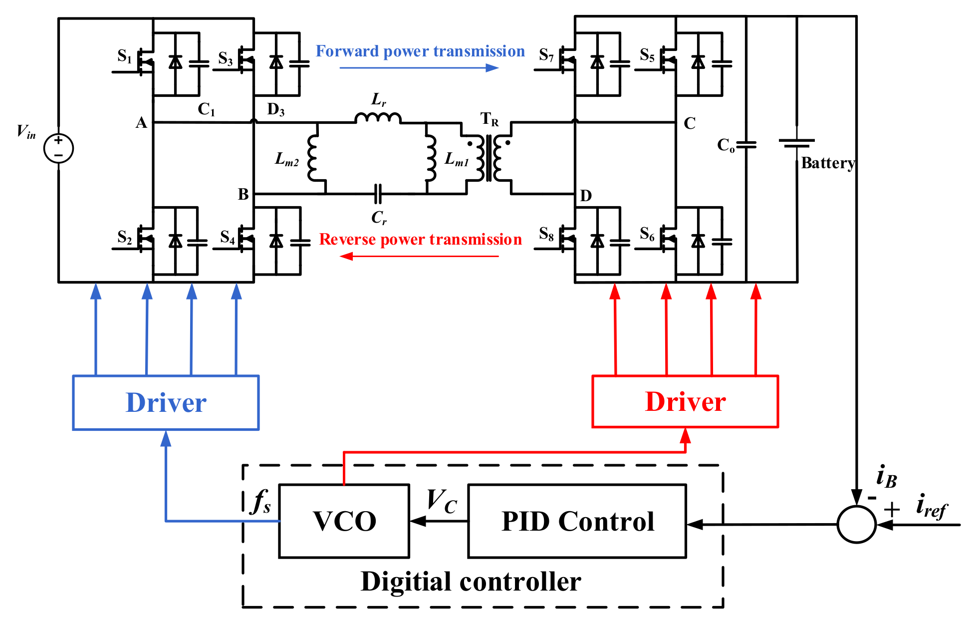
2. Working Principle of the L-LLC Resonant Bi-Directional DC-DC Converter
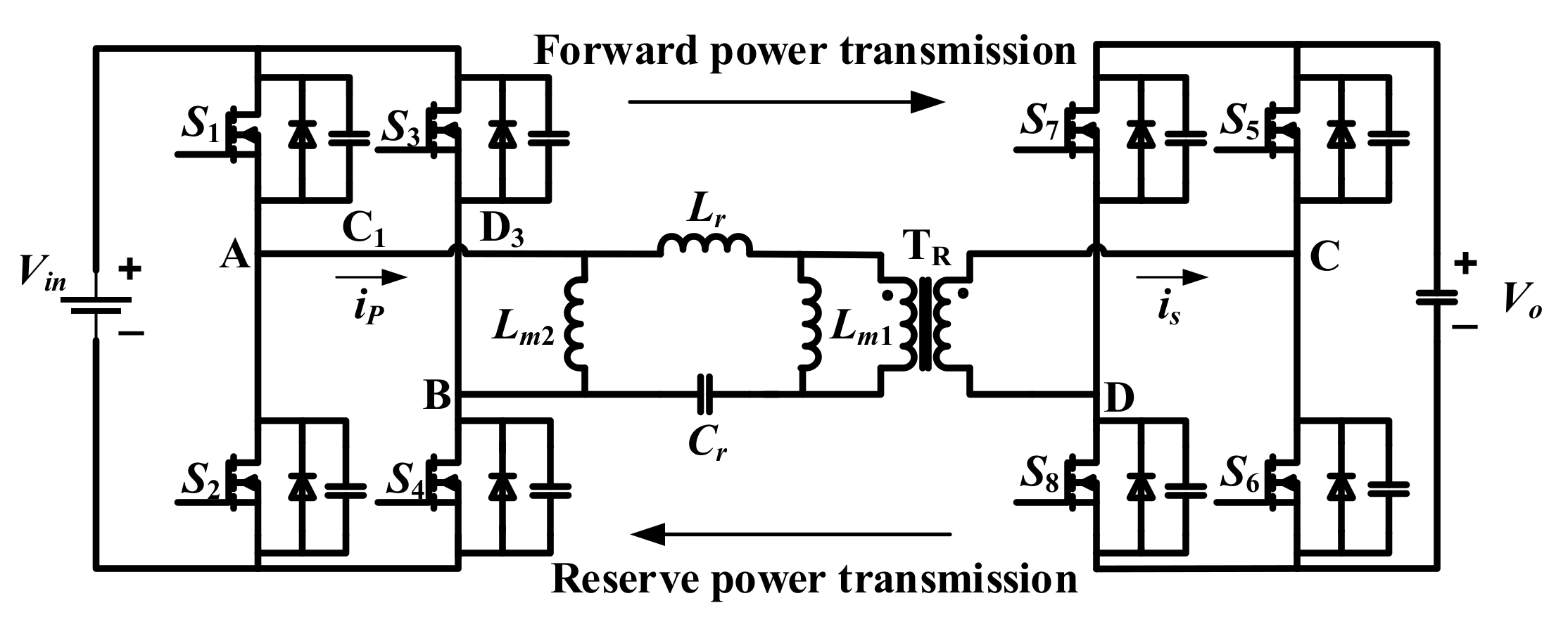
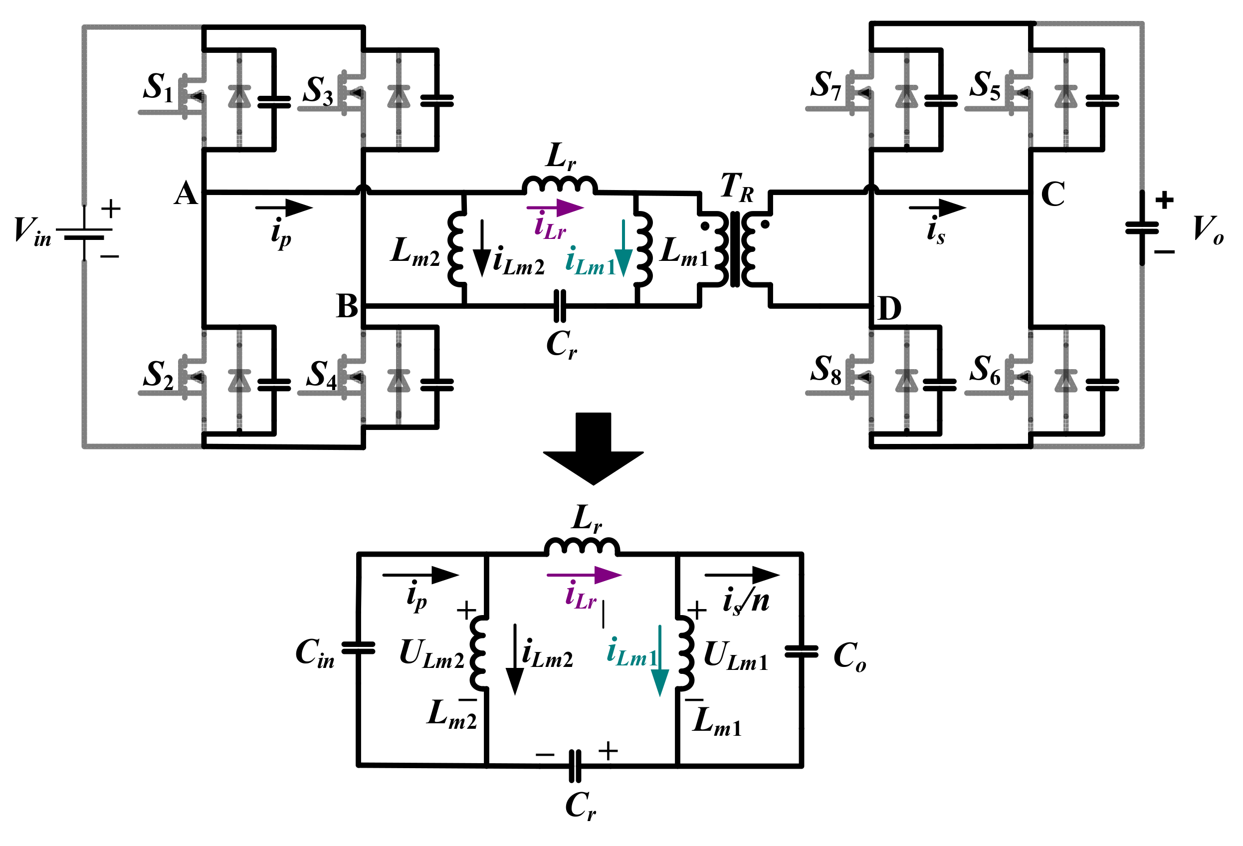
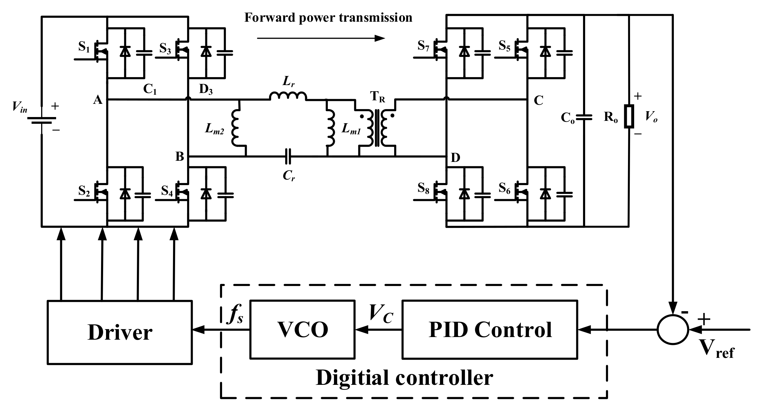
Figure 1 shows the topology of L-LLC-BDC, whose primary and secondary sides are connected to a full-bridge converter, respectively. Where
Vin and
VO represent the voltage of ESSs and the DC bus, respectively,
Lm1 represents magnetizing inductance of the transformer,
Lr and
Cr are resonant inductor and capacitor, and
Lm2 is the additional inductor.
S1–
S4 and
S5–S8 are switches on the primary and secondary converter, respectively.
D1–
D8 and
C1–
C8 are body diodes and output capacitors corresponding to
S1–
S8. As indicated in
Figure 1, the forward power direction is defined as from the primary side to the secondary side. To simplify the analysis as well as control,
Lm2 is set the same as
Lm1 so that the working principles in forward and reverse power direction are exactly the same. Therefore, only the working principle analysis in the forward mode is provided. In the forward mode, the output voltage is regulated with the frequency modulation method. When the converter works in the continuous conduction mode,
Lr and
Cr form a resonant tank, while in the discontinuous conduction mode,
Lm1 and
Lm2 participates the resonance in the forward and reverse mode, respectively. For example, in the forward mode, the
Lm2 does not participate in the resonance, but it helps the switches on the primary-side switch to realize ZVS. Therefore, so does
Lm1 in the reverse mode.
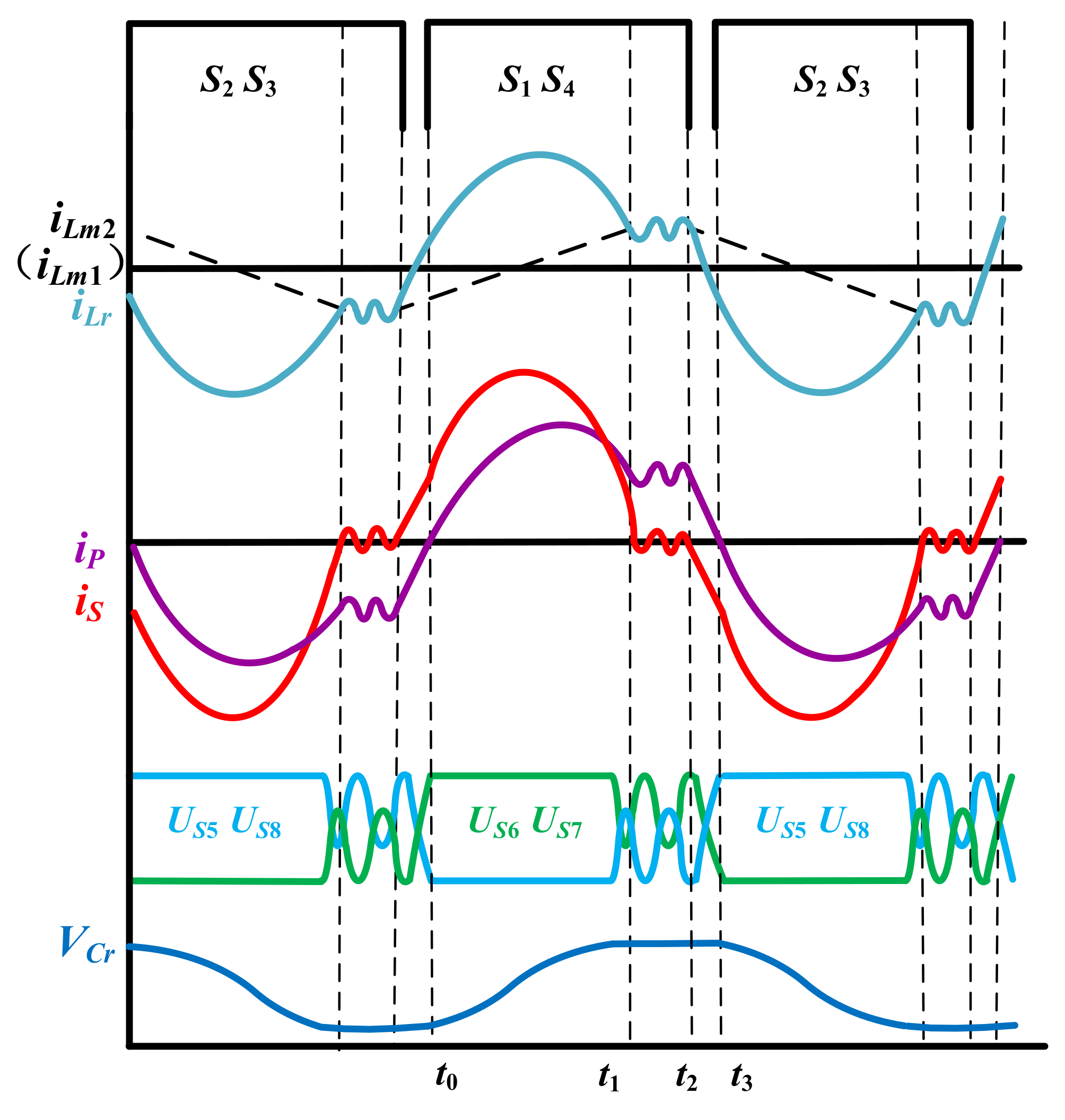
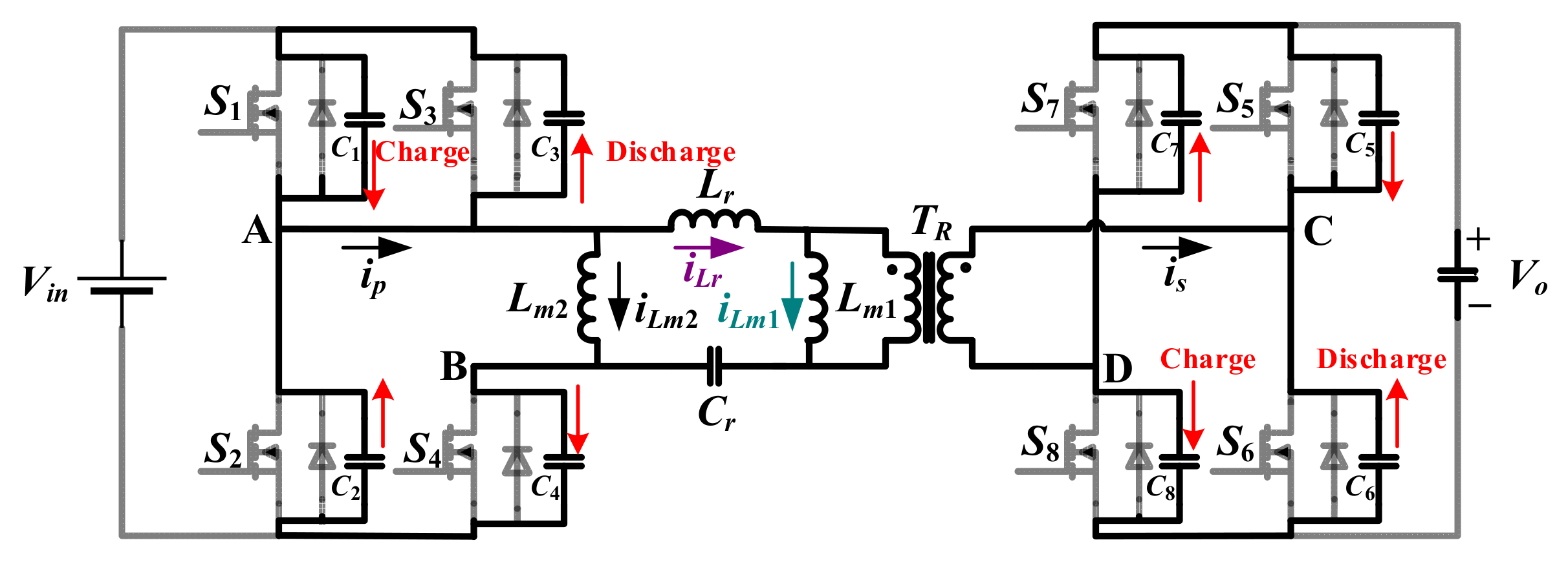
Considering the influence of the MOSFET output capacitor on the working process of L-LLC-BDC,
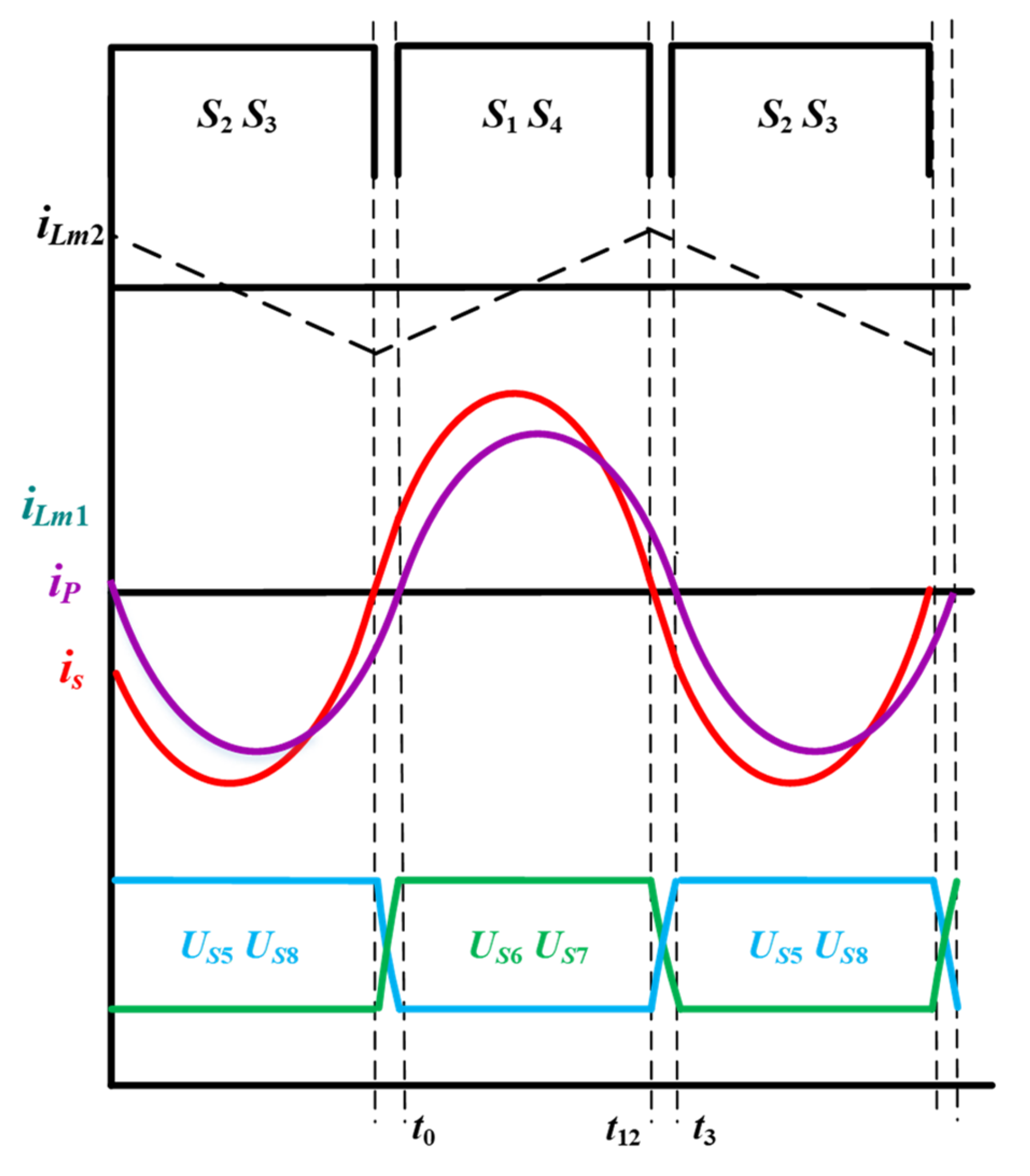
Figure 2 is intended to show the main steady-state waveforms of the converter, according to the status of the switches, and there are a total 6 modes. Due to the symmetric waveforms in the positive and negative period, the working principles in these periods are similar, only the analysis in the first half of the cycle is provided in this paper. The primary side currents are
ip =
iLr +
iLm2 and
is =
n (
iLr −
iLm1).
2.1. Mode I
Mode I:
t∈ [
t0,
t1] (see
Figure 2), during which switches
S1 and
S4 are turned on. Before
t0, the output capacitors of the switches
S1 and
S4 discharge to zero voltage through
ip, thus the switches
S1 and
S4 can be turned on under the ZVS condition,
vAB =
Vin. The body diodes of the secondary side switches
S5 and
S8 are conducted, which clamping
vCD =
VO energy is delivered to the load.
2.2. Mode II
Mode II:
t∈ [
t1,
t2] (see
Figure 2), during which switches
S1 and
S4 are still turned on,
Lr and
Lm1 resonate with
Cr, the resonant current is equal to the magnetizing current and the secondary side current
is is zero. With the current being zero, the body diodes
D5 and
D8 are shut off naturally without reverse recovery loss, realizing ZCS of the secondary switch. The output voltage no longer clamps the two points of C–D, and the output capacitor
C5–
C8 participate in the resonance. This mode is actually a continuous current stage.
2.3. Mode III
Mode III:
t∈ [
t2,
t3] (see
Figure 2), during which switches
S1 and
S4 are off, entering into the dead time. The
ip charges the
C1 and
C4 until their voltage reach to
Vin meanwhile.
C2 and
C3 discharges and their voltage drops to zero, which enables
S2 and
S3 to be turned on under the ZVS condition. The secondary current
is charges
C5 and
C8 to a voltage of
VO, and the voltage
S6 and
S7 decreases to zero. At the end of this stage, after the charging and discharging, the voltage at A–B is −
Vin, and the voltage at C–D is clamped at −
VO.
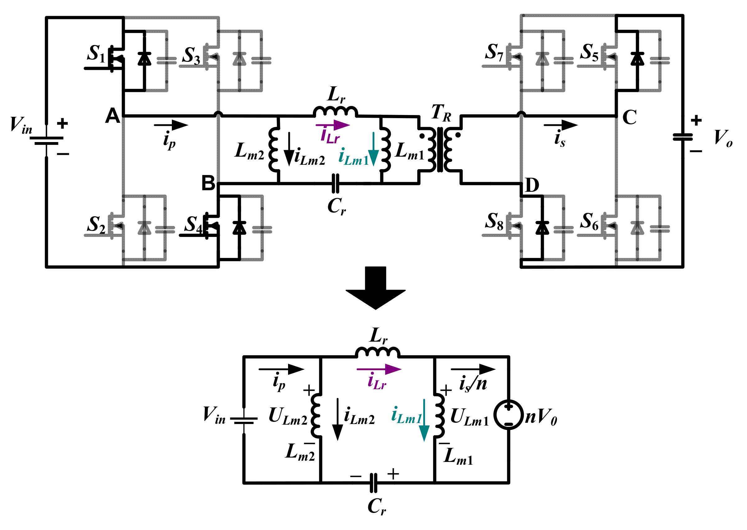
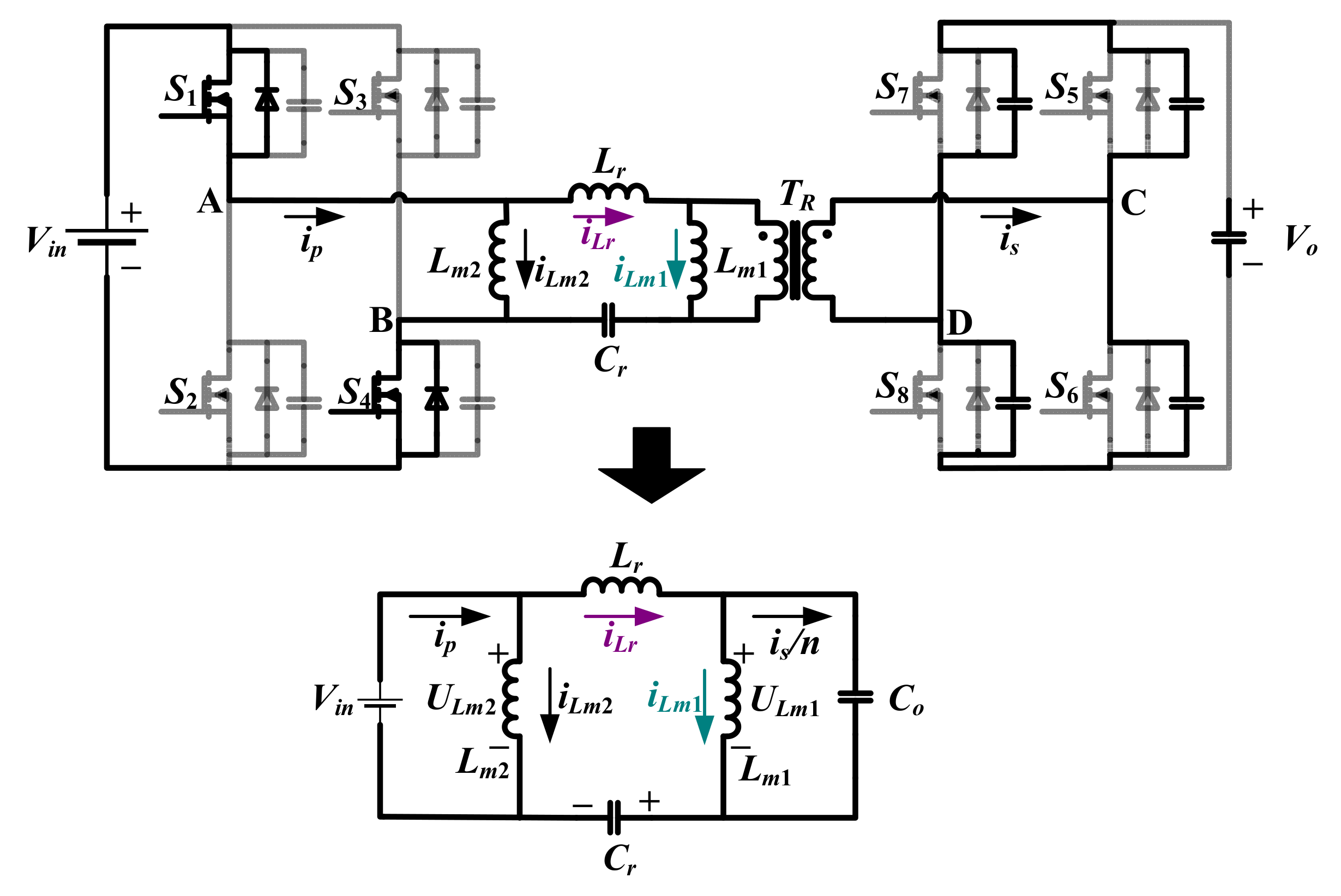
Figure 3,
Figure 4 and
Figure 5 show the equivalent circuits for Modes I, II and III and the differential equations are established, respectively, and we can get the expression of resonant inductor current and resonant capacitor voltage.
4. The Parameter Optimization Design of L-LLC Resonant Bi-Directional DC-DC Converter
It can be seen from
Figure 2 and the mathematical analysis for each working mode that the output capacitor of the switch participates in the operation of the circuit only in Mode II and III. When
t1 <
t <
t2,
vCD is no longer clamped to
VO, the output capacitors of the switches and
Lm1 form a resonant tank, which results in the high frequency oscillation at both primary and secondary side switches. Such, oscillation not only increases the conduction loss of the switch, but also affects the charging and discharging of the output capacitor during the dead time., i.e.,
t2 <
t <
t3. At the dead time, both side switches are disconnected,
C1–C4 and
C5–C8 are charged by
ip and discharged by
is, respectively. To maintain the same topology in forward and reverse modes, parameters such as the output capacitance of MOSFET are kept to be symmetric, so that capacitance referred from the secondary side is equal to that on the primary side. The decrease of the primary side current
ip will affect the soft switch of the converter. If the primary side current flows in reverse and drops the zero before the end of this period, the capacitors cannot be fully discharged, which results in the failure of the primary side switch to realize ZVS. Moreover, the change of current in dead-time makes the converter continue to a continuous current stage even when the switching frequency equals the resonant frequency.
The effect of the aforementioned output capacitor of MOSFET toward the operation of the converter can be eliminated by parameter optimization to improve the performance of the converter. The first consideration in the design of the resonant component is to reduce the loss of the converter to improve its efficiency. As L-LLC-BDC has the characteristic of the natural ZVS soft switching, the conduction loss accounts for a major part. It was testified that the current circulation can be reduced by increasing the magnetic inductance. However, there are trade-offs, with the increasing of magnetizing inductor, its current will be decreased, which prevents switches from achieving ZVS soft-switching.
As can be seen from
Figure 2, the voltage variation range of the output capacitance is the largest in the dead time, large
ip and
is are required for charging and discharging the capacitance. In practice, due to the presence of the stray inductance in the circuit, the voltage and current oscillation in the stage of Mode II are both attenuated. Therefore, the design should be based on the first zero crossing of
is to guarantee the ZVS soft-switching. Then, there is no operating Mode II.
According to the optimization goal of L-LLC-BDC, the starting point of the proposed improvement design method is to ensure that the magnetizing current fully charges and discharges the output capacitor of the switch within the dead time
Td, so as to achieve ZVS. From
uC2 (
t3) = 0,
uC6 (
t3) = 0, namely
From Equation (5), the peak magnetizing current can be obtained:
It can be seen from Equation (6) that with the selected device and given dead time, the peak magnetizing inductor current
Im can be obtained. When
ip and
is fully charges and discharges the primary side output capacitor and secondary side capacitor of the switch within the dead time, the waveform of the converter is the same as
Figure 7.
This is the resonant mode of the converter, and the resonant frequency is slightly higher than the resonant frequency. Under this condition, the charge and discharge of the capacitors are completed in the dead time, but due to the current on the additional inductance, the primary switch can realize ZVS completely. The resonant current has little distortion when the switch is turned on, and the expressions of the primary and secondary side current in the period
TB (from
t0 to
t12) can be obtained. Since the instantaneous value of
iLr at time
t0 is 0, and the instantaneous value of
iLr at time
t12 is
Im, then
is can be obtained:
The field current
iLm1 at
t12 in the period of Mode 1 can be linearly approximated as:
When the converter works in the resonant mode, energy from
is to the load within period as shown in the following expressions:
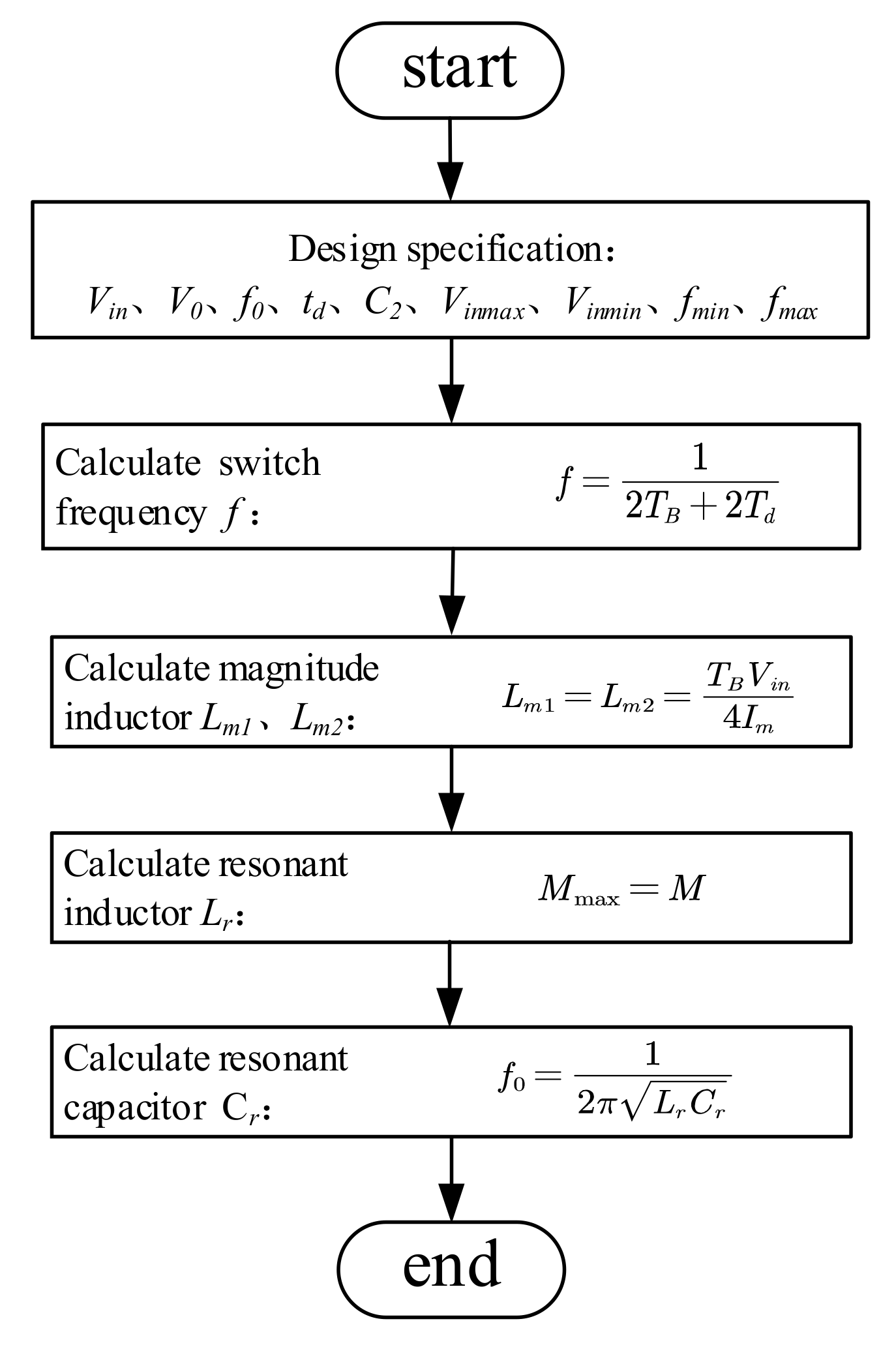
Given the resonant frequency f0, rated power PO, output voltage VO and dead time Td, the value of the period TB from t0 to t12 can be obtained. At this time, the ideal resonant frequency is f = 1/(2TB + 2Td).
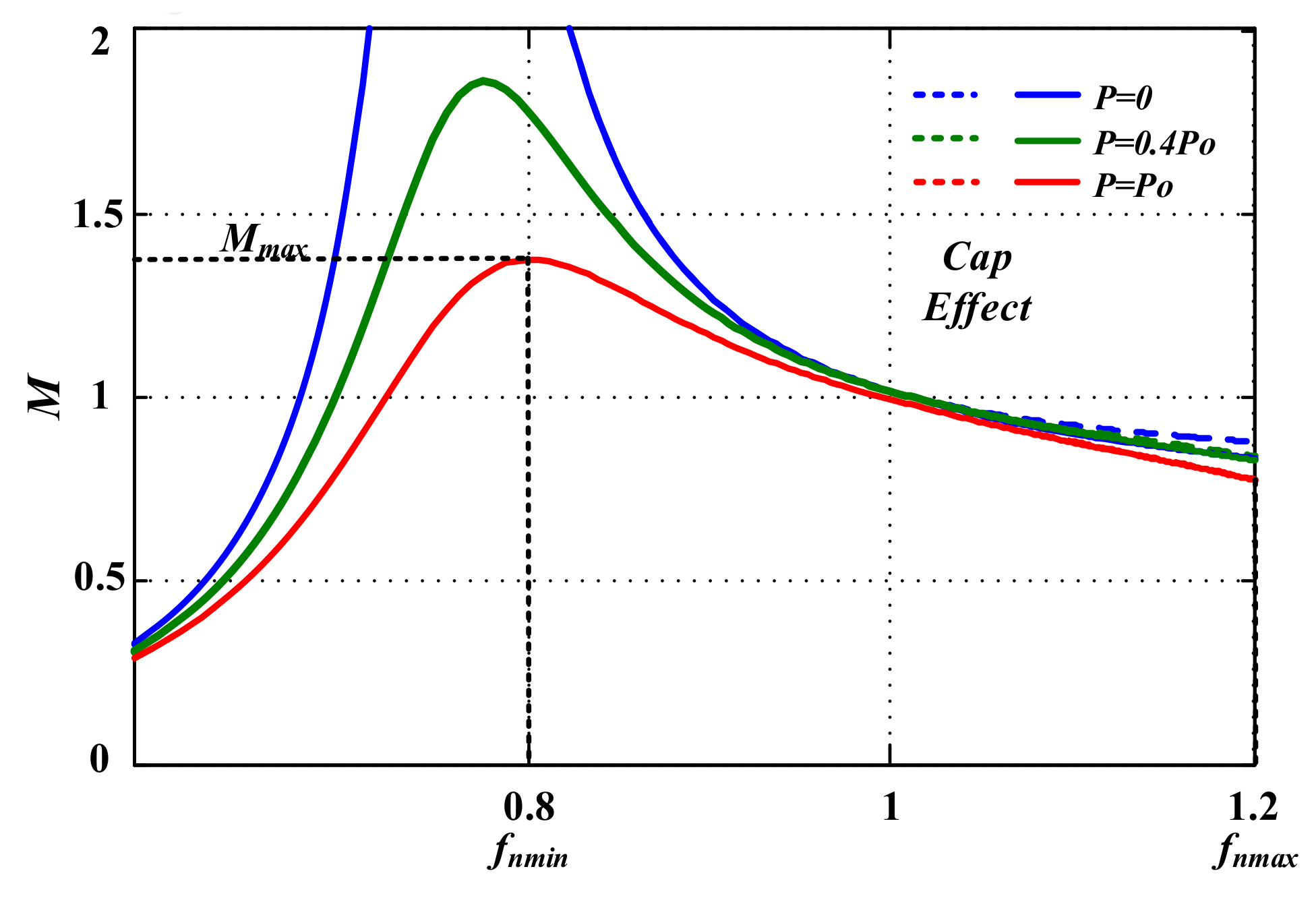
To analyze the effect of output capacitance toward the voltage gain
M, simulation studies are carried under the different switching frequency with and without output capacitance.
Figure 8 shows that voltage gain vs. switching frequency under the different load with the parasitic capacitance. Its characteristic curve is basically the same as that of the converter that does not consider the output capacitance. However, the gain has a sudden increase with the increase of switching frequency when there is no load or the load is very light.
In order to facilitate the calculation, the gain curve can be obtained without considering the transient expression of the output capacitance.
Appendix A shows the time domain equation when the converter operates at
fs =
f,
fs >
f,
fs <
f, respectively. The maximum gain
M can be obtained when the switching frequency
fs is the minimum.
According to reference [
9], the required maximum gain expressed by the minimum and maximum input voltages
Uinmax and
Uinmin is the maximum gain at full load:
where,
Mmax is the maximum gain which is achieved at full load when
fs =
fmin. More details of
Mmax can be found in Equation (A1).
Uinmax and
Uinmin are the maximum and minimum input voltage,
fmax is the maximum switching frequency.
As the Lm1 is known, the resonant inductance ratio Lr can be calculated from Equation (11), and the resonant capacitor can be derived by the resonant frequency f0. In practical design, the current and voltage oscillation in the continuous current stage can also be reduced by increasing the resonant capacitance value properly.
The optimum design flow is a simple mathematical expression, the design flow of L-LLC-BDC resonance parameters is shown in
Figure 9.
According to the initial conditions, the RMS current expressions of the magnetizing inductance
Ip and the additional inductance
ILm1 and
ILm2 at the quasi-resonant frequency are as follows:
As the ideal resonant period is less than the resonance period, i.e., TB < T0, the optimal Lm1 (meaning the magnetic inductance is large enough) is calculated according to charging and discharging of the output capacitance of the switch in the dead time. When the output voltage and the load is constant, the effective value of the primary side current Ip and the effective values of the magnetic inductance current as shown in expressions Equation (12) will decrease, leading to improved efficiency of the converter. Even working at the other frequency, the reduced magnetizing current can also improve the efficiency of the converter.
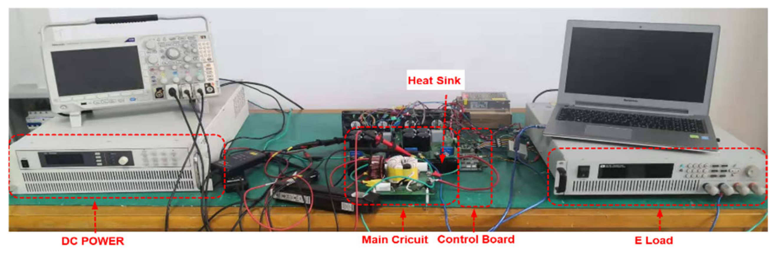
5. Experimental Verification
To verify the optimization design method proposed in this paper, the prototype of L-LLC resonant bidirectional DC-DC converter is built. The overall experiment set-up is shown in
Figure 10.
The input voltage varies from 630 V to 890 V, while the output voltage is 380 V. The operating frequency range is 80–120 kHz, the actual working resonant frequency
f is 104 kHz, dead time is 100 ns, and output capacitor is 92 pF. A 220 pF capacitor is connected in parallel to the secondary side switch to ensure the forward and reverse topology of the converter are exactly the same. The all SiC MOSFET are mounted on the heat sink, and adopts air cooling at the same time. The comparison between parameter II before [
1] and after optimization is listed in
Table 1.
To regulate the output voltage, a feedback controller is designed.
Figure 11 shows the simplified control block diagram. A conventional linear regulator, such as PI compensator, controls the switching frequency to regulate the output voltage
VO to deal with the load change. The pulse frequency modulation (PFM) is applied to the converter, and the control system is built in TMS320F28335.
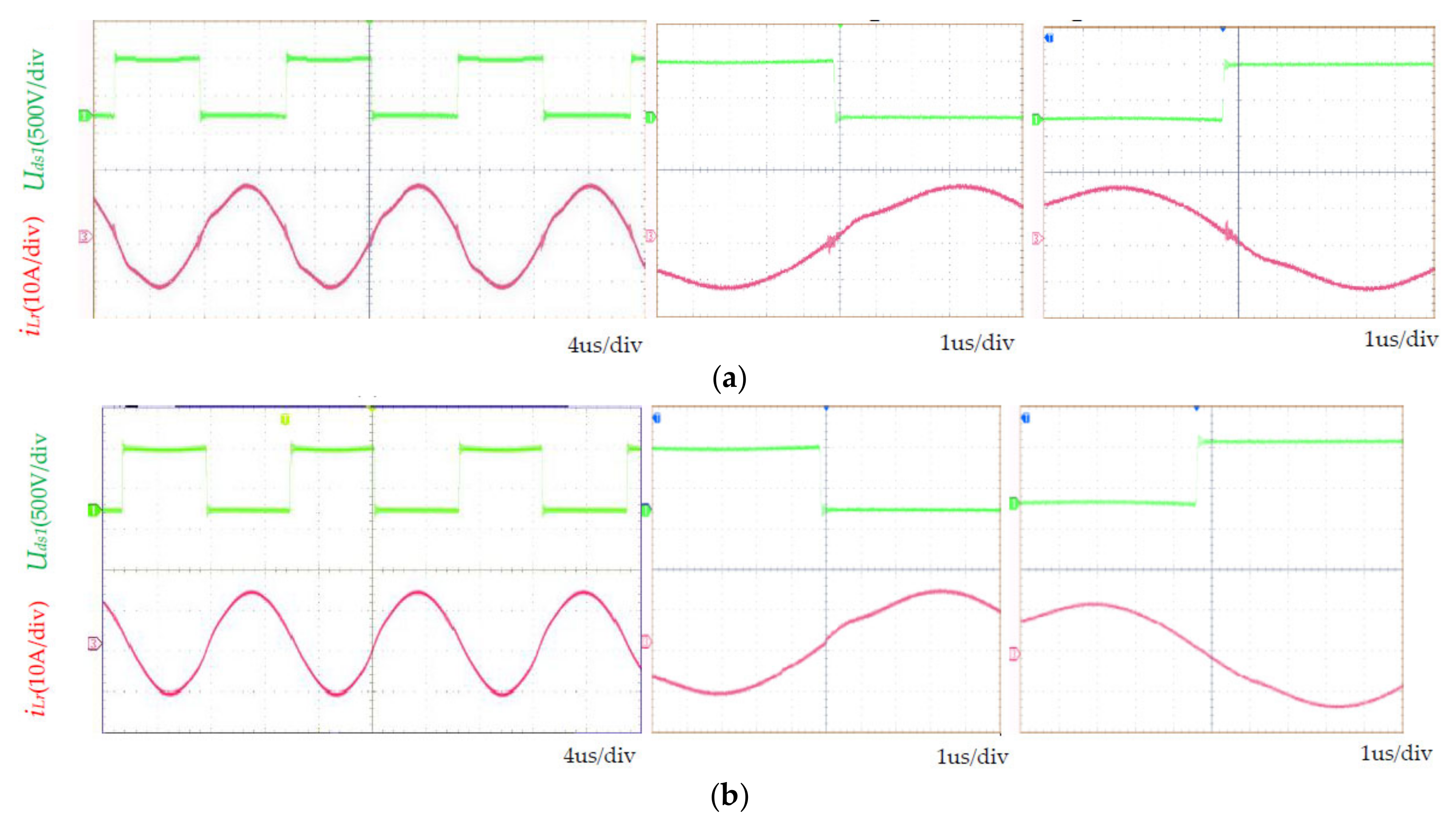
5.1. Steady State Waveforms
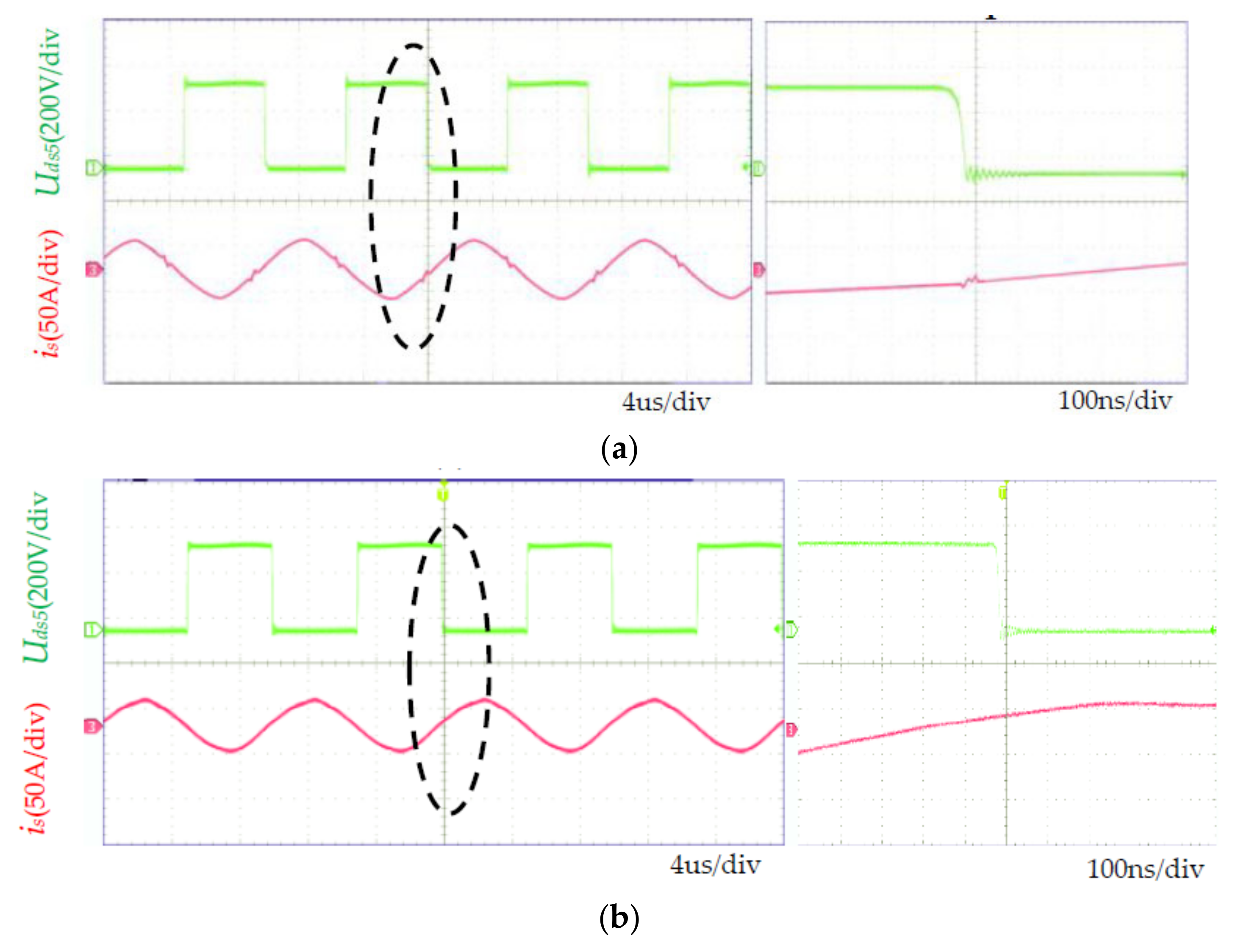
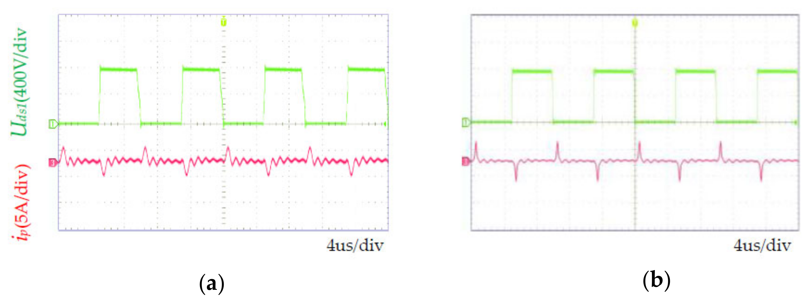
The waveforms of the voltage
Uds1 at both ends of the primary side switch which work with the forward direction and the primary side current
iLr and their detailed waveforms are shown in
Figure 12. As shown in
Figure 12a, when the switch is off, there is high frequency oscillation before the parameter’s optimization because the capacitor of the switch is not fully charged or discharged during the dead time. It can be seen from
Figure 12b that in the continuous flow stage, the output capacitance of
S1 is fully discharged in the dead time, the oscillation has been significantly reduced compare what is shown in
Figure 12a, which validates the effectiveness of the parameter optimization. The waveforms of the voltage
Uds1 at both ends of the primary side switch that work with the forward direction and the primary side current
iLr and their detailed waveforms are shown in
Figure 12. As shown in
Figure 12a, when the switch is off, there is a high frequency oscillation before the parameter’s optimization because the capacitor of the switch is not fully charged or discharged during the dead time. It can be seen from
Figure 12b that in the continuous flow stage, the output capacitance of
S1 is fully discharged in the dead time, and the oscillation has been significantly reduced compare the shown in
Figure 12a, which validates the effectiveness of the parameter optimization.
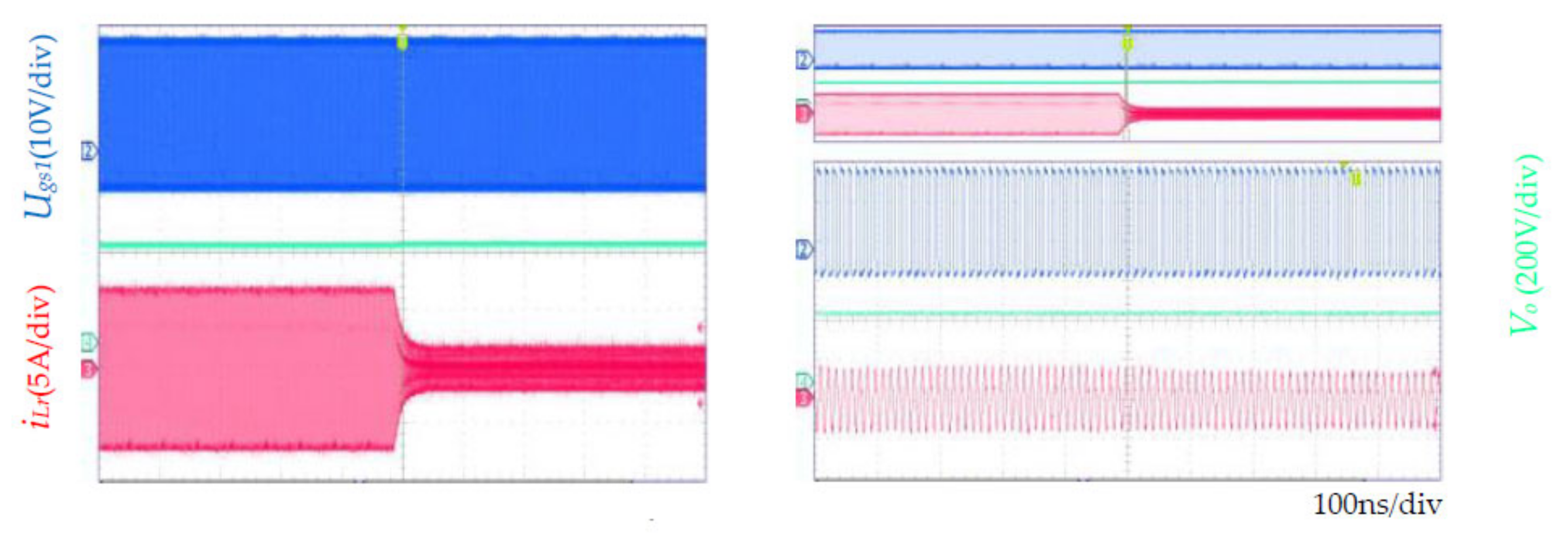
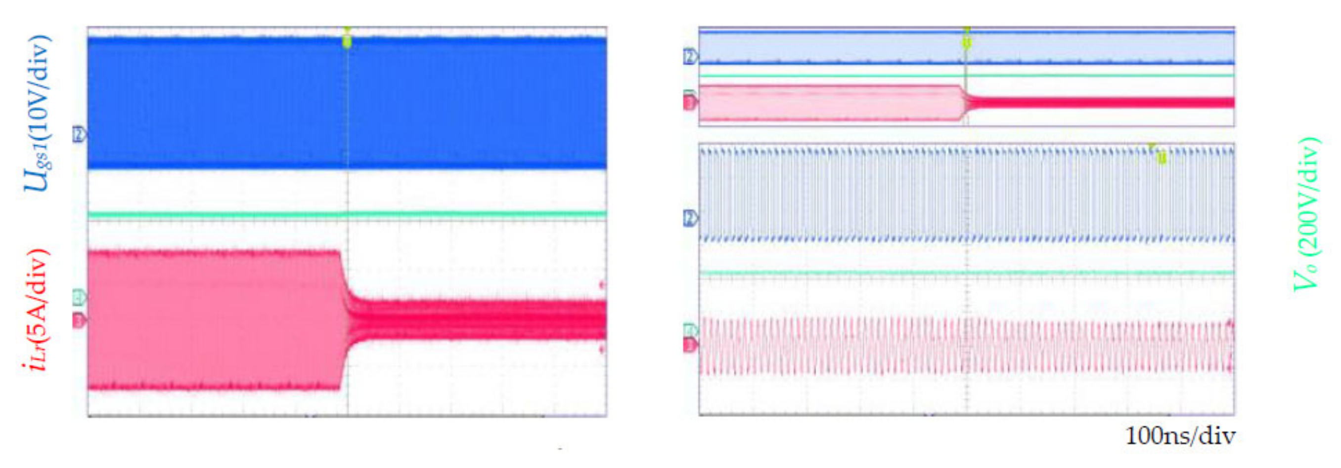
5.2. ZVS Soft Switching
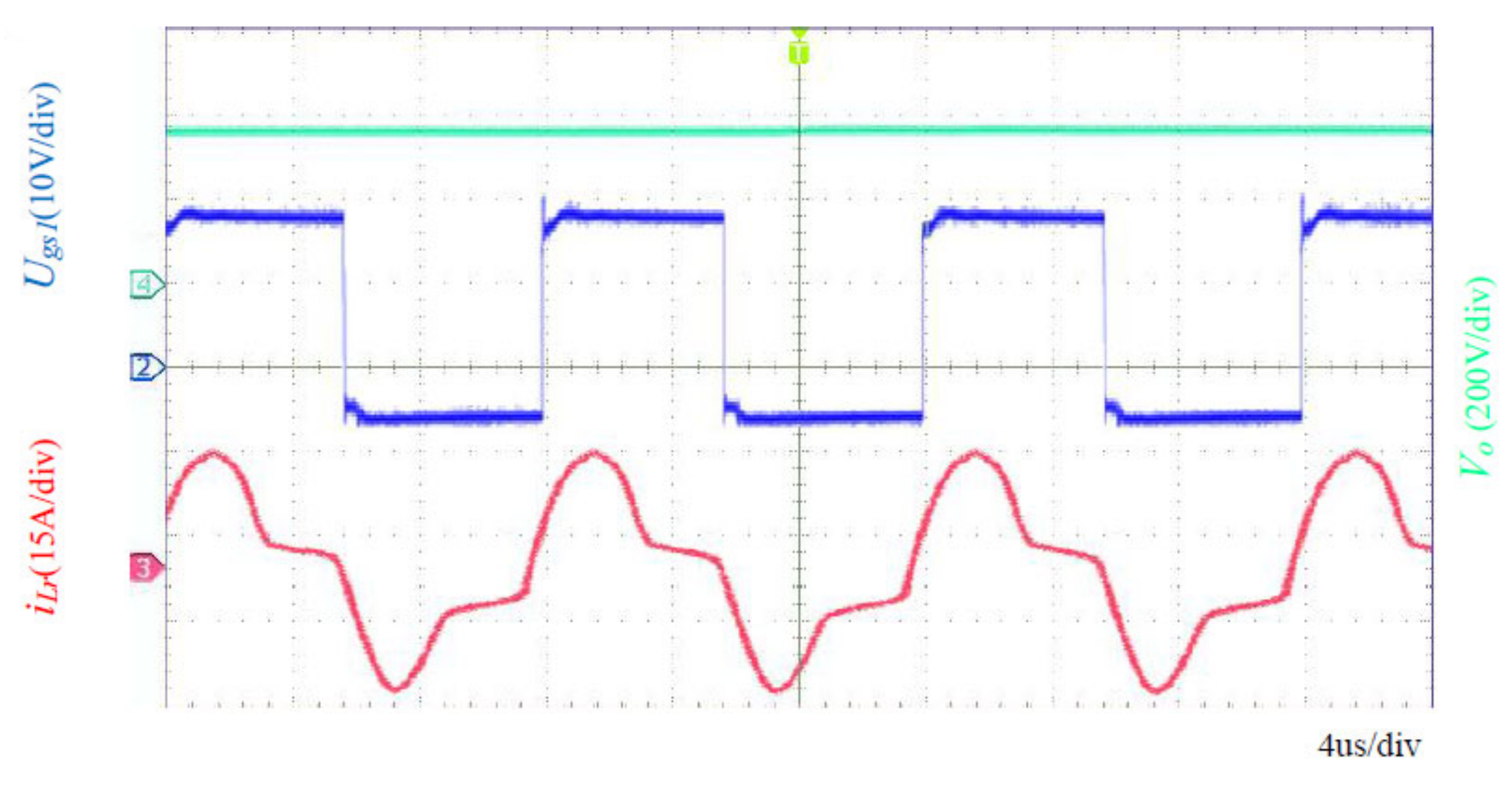
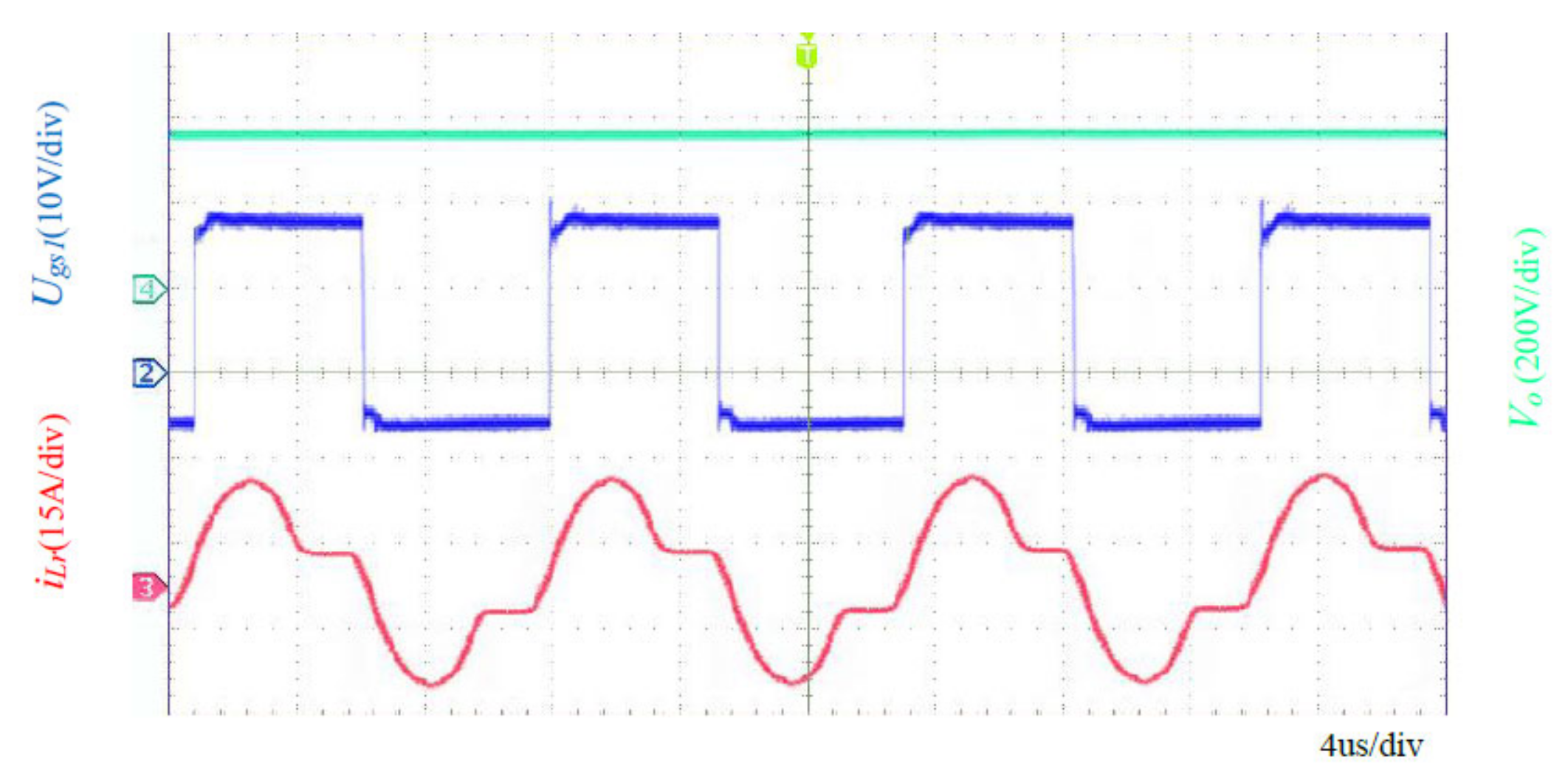
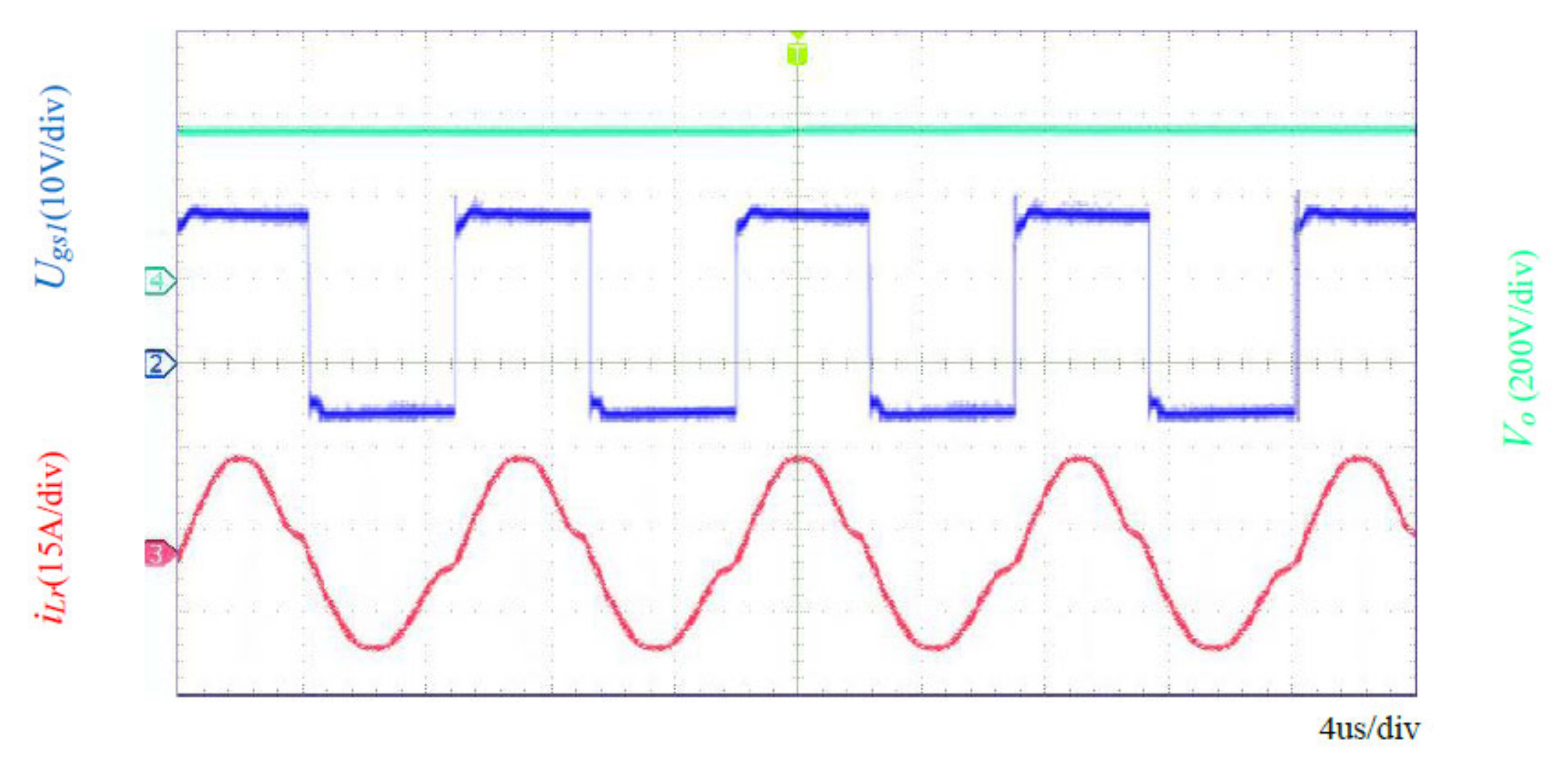
Figure 13,
Figure 14 and
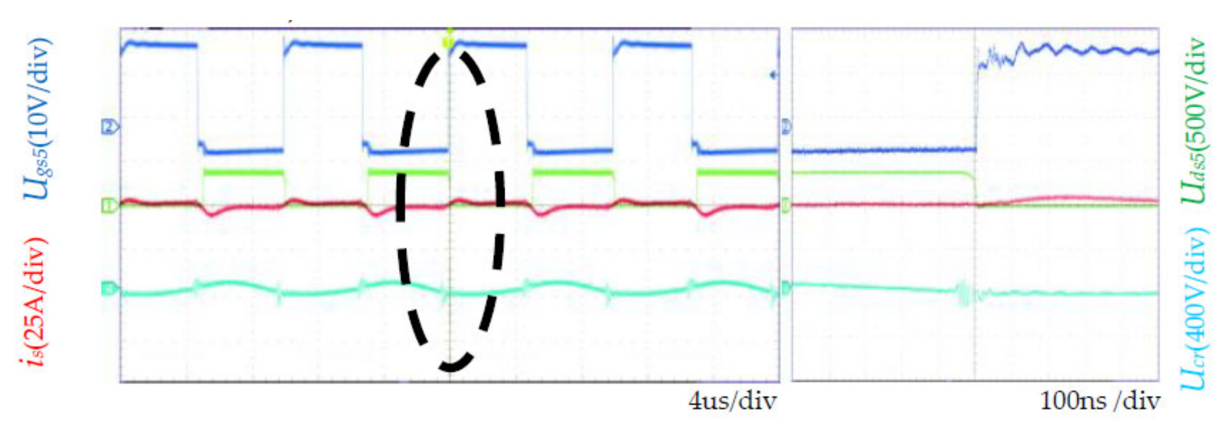
Figure 15 show the experiment waveforms with the reverse transmission when the converter is half loaded, lightly loaded, and fully loaded, respectively.
Figure 13 shows the driving waveforms of switch, the waveforms of the voltage
Uds5 at both ends of the primary side switch that works in the reverse direction at light load, the primary side current
is, the resonant capacitor voltage
Ucr, and their detailed waveforms. As can be seen from
Figure 13,
Figure 14 and
Figure 15, the ZVS is achieved in a wide range of loads, e.g., the ZVS is achieved when the output current is 0.4 A, 4 A and 8 A.
Similarly,
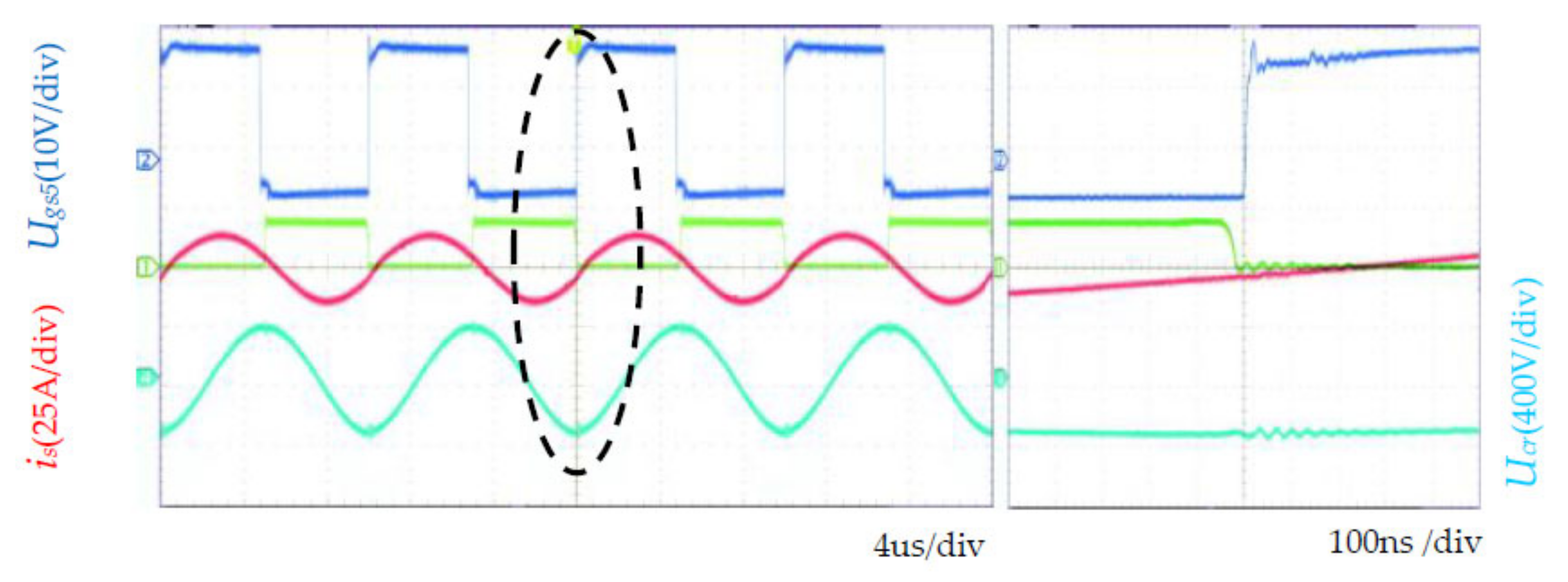
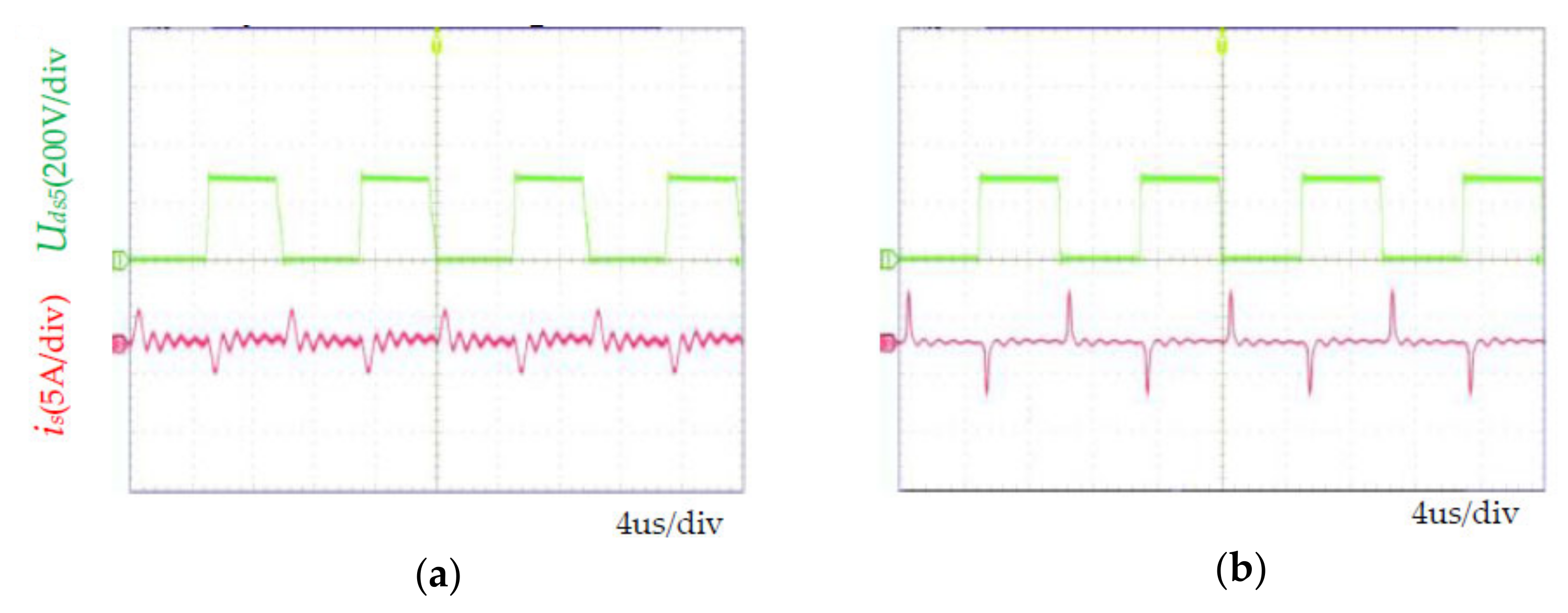
Figure 16 compares the waveforms of the secondary side with and without optimization.
Uds5 has oscillation in the forward direction, which is caused by the parasitic oscillation between the resonant inductor and the MOSFET parasitic capacitor when all switches are turned off after half a resonant period.
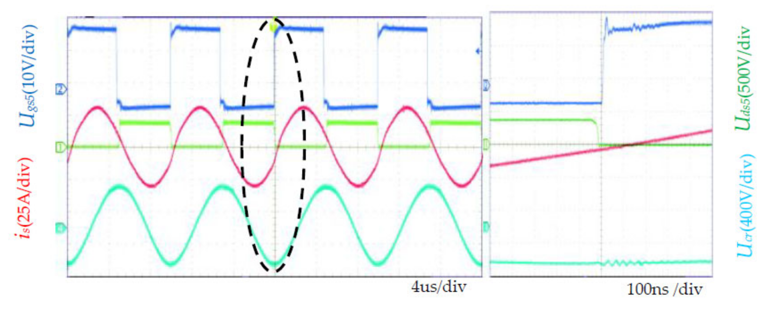
Figure 17 shows the waveforms of the voltage
Uds5 and the secondary side current
is when the load current is 0.4 A in forward transmission power. The waveforms of the voltage
Uds1 of the secondary side switch
S1, and the secondary side current
iP when the load current is 0.4 A in reverse transmission power is shown in
Figure 18. It can be seen that both voltage and current oscillations are decreased with forward transmission and reverse transmission significantly after the optimization.
5.3. Dynamic Waveforms
Figure 19 and
Figure 20 show the waveforms of the output voltage and the resonant current
iLr when load step-up and step-down with forward transmission power by PID closed-loop control. The pulse frequency modulation (PFM) is applied to the converter, the control system is built in TMS320F28335, and control the switching frequency to regulate the output voltage
VO. According to the figure, the output voltage is constant at 380 V, indicating that L-LLC resonant bidirectional DC-DC converter has the ability to keep the output voltage constant under different loading conditions.
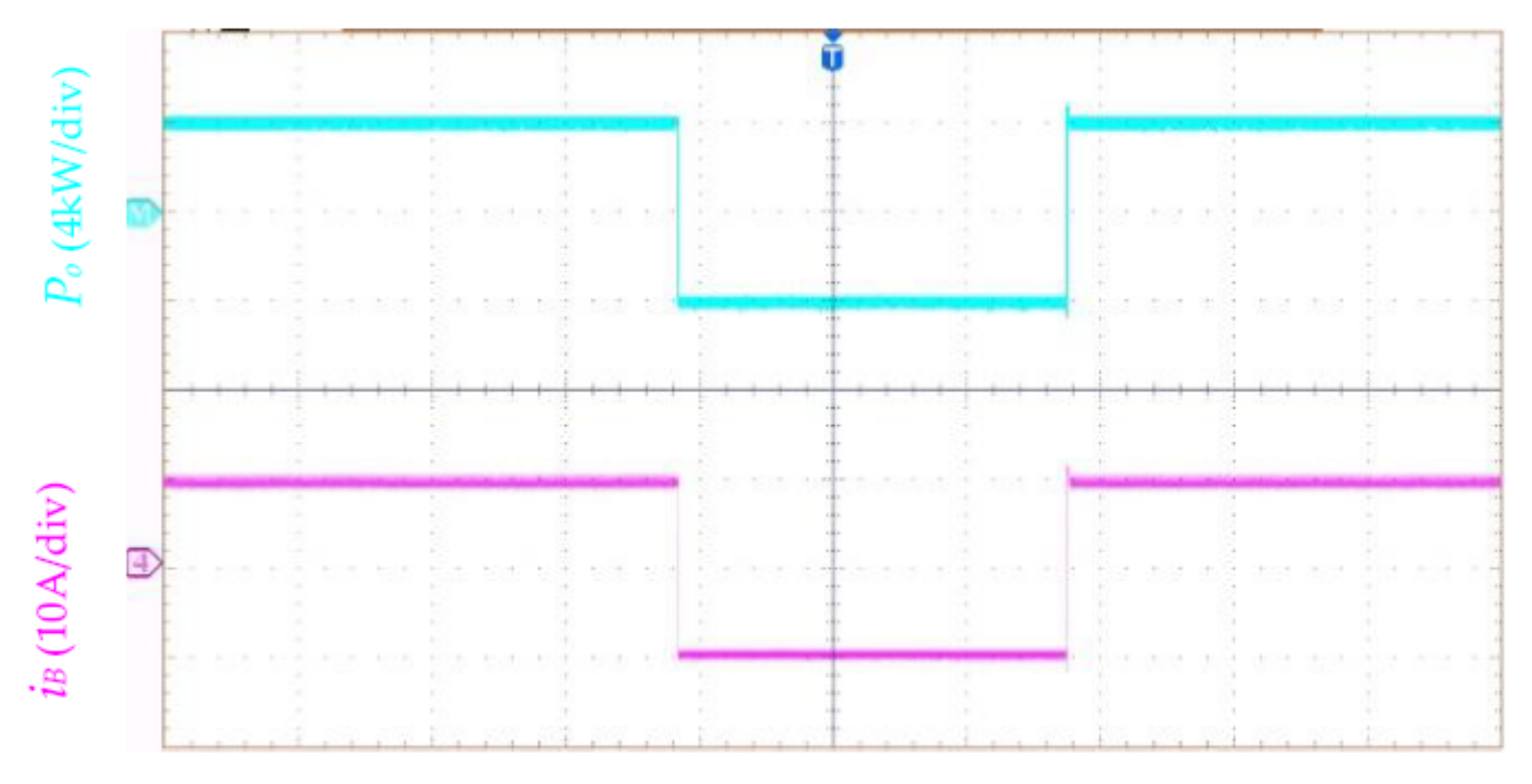
In order to carry out a bi-directional power transmission experiment, the control block diagram of charging and discharging battery experiment system is designed, as shown in
Figure 21. When the reference current is −10 A, the DC power supply charges the battery, the converter operates in forward power transmission. When the reference current is 10 A, the battery is discharged to the DC power supply, and the converter runs in reverse. The dynamic waveforms of the charging and discharging battery are shown in
Figure 22. The figure shows that the charge and discharge current can follow the reference, and forward and reverse power flow can be achieved.
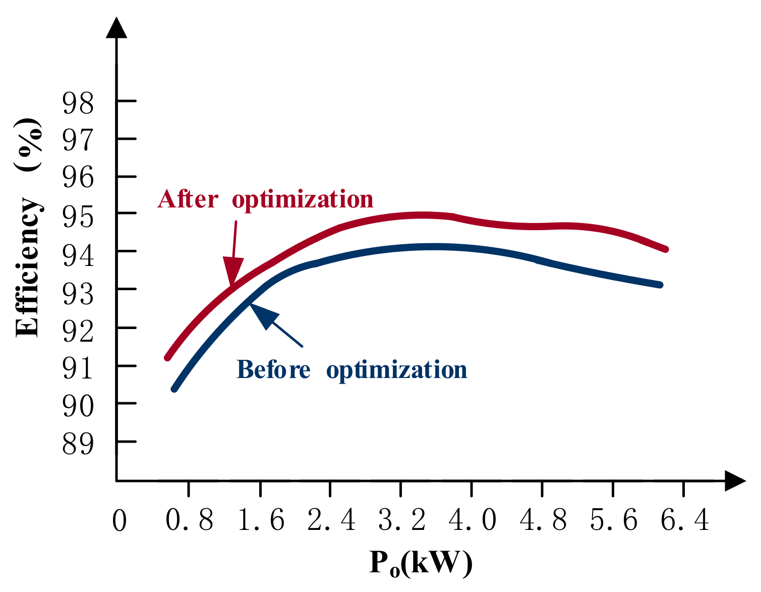
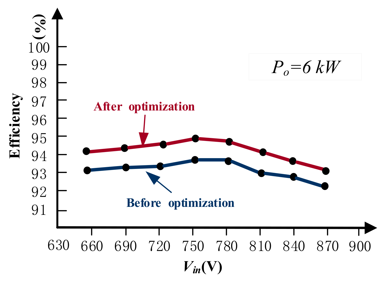
5.4. Efficiency
The operation efficiency is measured by a power analyzer under different input voltage levels and load conditions, and electronic load is used for load regulation.
Figure 23 and
Figure 24 show the efficiency curves of the design method under different loading conditions with forward and inverse transmission power. As can be seen from
Figure 23 especially, when the output power is 3 kW, the maximum efficiency of the experimental device can reach up to 94.9% with forward transmission power. The design method that has been optimized delivers improved loading efficiency compared with that in the literature [
4]. This is due to uncontrolled rectifier is used in the secondary side to reduce the driving loss and maximum magnetic inductance also reduces the turn-off current of the switch. In particular, light or moderate loading efficiency is 1% higher than that in the literature [
4], because the time domain analysis method is taken to obtain the maximum value of
Lm1, which is independent of load change. The loss ratio
iLm1 increases under light load, so the efficiency increases greatly under light load. The oscillation at full load is significantly reduced, and the efficiency is increased.
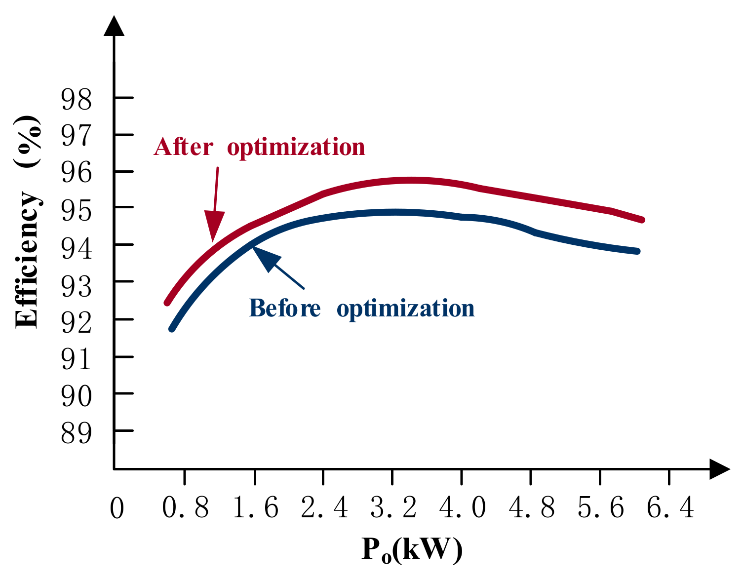
The output voltage of the converter is constant by adjusting the frequency when the input voltage changes. The ideal switching frequency of the converter is 104 kHz when the input voltage is the rated voltage 760 V. The experiment waveforms are given in
Figure 25,
Figure 26 and
Figure 27 showing resonant current and output voltage at full load.
The figures show that the optimized parameters in this paper can realize the closed-loop control of the converter by adjusting the frequency of the switch under different input voltages.
Figure 28
shows the operation efficiency of L-LLC-BDC resonant converter in forward mode under the different input voltage. The efficiency can reach up to 96% at rated power with an input voltage of 760 V.
From reference [
26], for the Sic device, the ratio of hysteresis energy loss
Ediss and Coss stored energy
Eoss is less than 0.1, even to 0.01. The device selected in this paper is C2M0080120D,
EOSS is 27 μJ when the input voltage is 760 V from the datasheet, so the maximum hysteresis energy loss
Ediss is less than 2.7 μJ, even to 0.27 μJ, and maximum hysteresis loss of a single device is 0.27 W when the switching frequency is 100 kHz, even to 0.027 W. The proportion of the hysteresis loss is very small for the 6 kW converter.
Switching loss includes turn-on loss and turn-off loss. (1) Turn-on loss: The resonant converter achieves soft switching, which ideally yields zero losses, but various studies show that even if the soft switching is realized, there is hysteresis loss in the switch. The loss is very small by analysis quantitatively in the second question. (2) Turn-off loss: The turn-off loss of the switch in the primary side is about 2 W, turn-off loss of the switch in the secondary side ideally yields zero because the ZCS is realized when the converter operates at the main mode. In the actual state, Coss transfers most loss to the conduction loss, However, the overall loss of the switch remains unchanged.
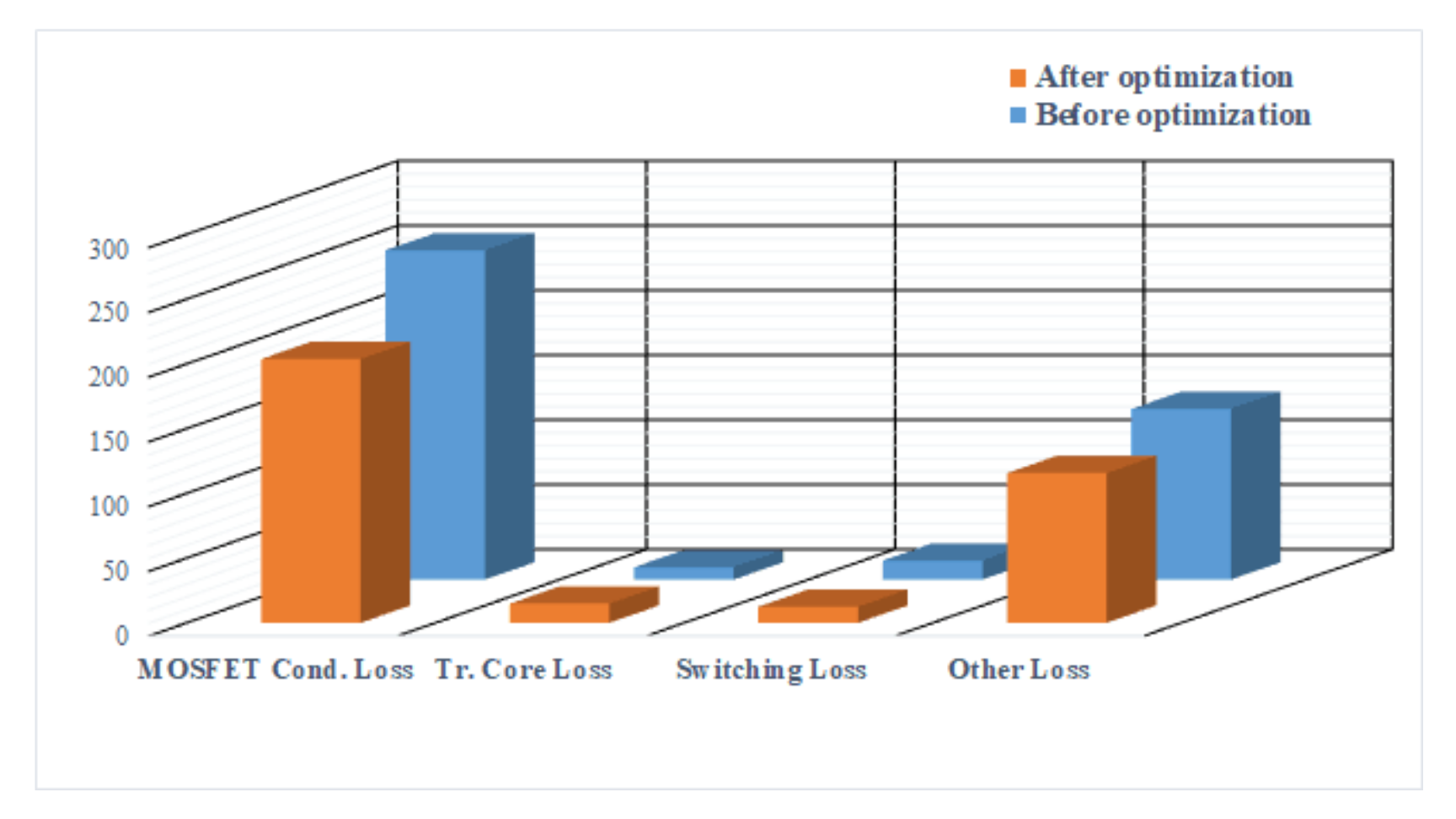
The main loss of the resonant converter is the conduction loss of the switch. The efficiency is improved because the current value passing through the switch of primary side is reduced in the design. Due to the large magnetic inductance of the transformer, the core loss of the transformer is slightly larger than that before optimization.
The power loss distribution and comparison of the before optimization and after optimization have been done and presented in
Figure 29, and the loss breakdown has been down at full load and 760 V input.


