Article

Space Charge Accumulation at Material Interfaces in HVDC Cable Insulation Part I—Experimental Study and Charge Injection Hypothesis

1
Department of Electrical Engineering, Chalmers University of Technology, SE-41258 Gothenburg, Sweden
2
Nexans Norway AS, 70 Knivsøveien, NO-1788 Halden, Norway
3
Nexans Research Centre (NRC), 69007 Lyon, France
*
Author to whom correspondence should be addressed.
Energies 2020, 13(8), 2005; https://doi.org/10.3390/en13082005
Submission received: 1 March 2020 / Revised: 7 April 2020 / Accepted: 14 April 2020 / Published: 17 April 2020

Abstract

:
On-site installation of accessories on extruded polymeric high voltage cables in a common practice. The procedure requires the shaping of the physical interface between the cable insulation surface and the pre-molded accessory body. On such interfaces, rough surfaces should be avoided in order to limit space charge accumulation in the insulation, which affects the cable performance by reducing insulation life-time, creating conditions for local field enhancement, and, respectively, the formation of possible breakdown path e.g. by electrical treeing. Space charge measurements on cable insulation peelings were undertaken to assess the space charge injection and accumulation on interfaces with varying degrees of surface roughness in order to improve understanding on this subject. The results of the measurements confirm the hypothesis regarding the enhancement of charge injection from rough surfaces when electric field strength exceeds a certain level. The accumulated charge density in the material is shown to strongly depend on the field strength and temperature in both polarization and subsequent depolarization measurements. These results emphasize that a bipolar charge transport model that incorporates field and temperature dependencies of charge injection, trapping, detrapping, and recombination processes needs to be adopted to accurately describe the observed electric conduction phenomena.

Graphical Abstract

1. Introduction

Controlling space charge accumulation in the insulation is a key aspect for ensuring reliable HVDC cable system performance, as enhanced charge accumulation might lead to premature failure and the initiation of electrical treeing in the material [1]. Therefore, limiting the amount of charge that is injected into the insulation is crucial. Within these systems, cable accessories, such as land joints, field joints, and terminations introduce physical interfaces [2] between the cable insulation surface and the pre-molded accessory component. A joint is illustrated in Figure 1, displaying this interface.
The cable surfaces are made on site by removing the outer semiconductive layer of a cable, followed by additional surface treatments. Different degrees of insulation surface roughness will be introduced in the physical interface, depending on the preparation method. Roughness is known to influence the local field distribution at the interface, locally enhancing or reducing the electric field due to the introduced micro-scale geometrical inhomogeneities [3,4]. In earlier work [5,6,7], such field distributions were assessed and their impact on Schottky and Fowler–Nordheim types of charge injection was evaluated. Figure 2 further exemplifies the work performed in the past and present studies.
The surface structure was measured through profilometry and implemented in COMSOL Multiphysics®, as indicated in Figure 2 [8]. Thereby, different distributions of the field enhancement factors (FEF) were found through solving Laplace’s equation on measured surface profiles [7], which were dependent on surface geometry (referred to as Laplacian field below). Such effects establish a geometric field distribution, as shown in Figure 3B, where, locally, the field enhancements intensify charge injection from their respective regions on the surface [3,4]. Such distributions are similar in their appearance to those that were found by Novikov [4], where an enhanced Fowler–Nordheim injection was also calculated for rough electrodes. These distributions thus give a statistical overview over local reduction (FEF < 1) and increase (FEF > 1) of the Laplacian electric field at the surface, as highlighted in Figure 3.
The accurate assessment of roughness and calculation of corresponding Laplacian field distributions (as shown in Figure 3B) is rather simple and straight-forward. The complexity arises when considering the space charge controlled fields, requiring assumptions regarding which types of injection and conduction mechanisms need to be accounted for. Furthermore, evaluating such mechanisms within the three-dimensional surface structure and assessing their impact on the local field distribution bring additional complexity. Therefore, it is the purpose of this work to describe this complex charge injection-transport balance in a simplified way utilizing a one-dimensional approach.
Specifically, the impact of roughness on Schottky and Fowler–Nordheim injection is considered, allowing for formulating a one-dimensional bipolar charge transport model. Being calibrated against the results of space charge measurements on samples with various degrees of surface roughness, such a model makes it possible to separately assess different physical conduction effects for such samples. Since the enhanced charge injection suggested earlier in [5,7] relies on the Laplacian field distributions, this work does not consider trapping, detrapping, and transport being affected by strong field variations (Figure 3A) found in the ~30 μm wide interfacial region.
After a review of the used methodology, the results are first summarized for the injection equations in Section 3.1, following a summary of space charge measurements in Section 3.2.

2. Materials and Methods

2.1. Sample Manufacturing

Space charge measurements were conducted while using cable peelings to ensure identical surface characteristics when compared to full-scale HVDC cable accessories. The manufacturing process began with preparing the insulation surface of a degassed and screened DC grade XLPE cable. The samples with the following surface characteristics were prepared: remolded, smooth abraded, abraded, and rougher abraded. These surfaces introduced different texture types and different degrees of surface roughness. Next, a rotational cutting tool was used to cut 0.4–0.5 mm peelings along the angular orientation of the cable. This resulted in a cut underside of the peelings, which is referred to as backside in this study. Such samples initially have low content of crosslinking byproducts, owing to cable degassing. They were additionally stored for 2–5 months in an incubator prior to space charge measurements, during which additional outgassing occurred. After storage, low contents of crosslinking by-products were present in such samples [9]. Thus, any observed effects could be attributed to electronic charge injection and transport.

2.2. Roughness Enhanced Charge Injection

In previous work [5], surface profiles that were measured by means of optical profilometry, were used to calculate the Laplacian field distributions in the surface layer. These field distributions shown in Figure 3B allow for evaluating the average injection current density while using the relation:
J a v g ( E ) = 1 A   A   J ( F E F · E ) d A ,
where A is the area of the investigated domain in m2 and FEF are the local, unitless field enhancement factors of the surface displayed in Figure 3B. In Equation (1), it is assumed that the local current density J(FEF·E) is dominated by the component, the direction of which coincides with that of the average field (i.e., the field produced by ideally smooth electrodes). Some errors are introduced as the local currents densities’ direction, being normal to the surface, is disregarded at each point on the irregular surface, due to this assumption. The resulting average current density Javg, is thereby a field-dependent, scalar measure of the charge entering the material at each time step. This averaging was done while assuming the Schottky mechanism of charge injection resulting in the (one-dimensional) current density:
J s ( F E F · E ) = λ R A 0 T 2 e ϕ B k T e e k T ( e ( F E F · E ) 4 π ε 0 ε r ) .
here, λR is material specific correction factor, here being arbitrarily chosen as 0.7; kB is Boltzmann’s constant in eV/K; T is the absolute temperature in K; e is the elementary charge in C; φB is the barrier height in eV; A0 is the Richardson’s constant in Am−2K−2; E is the electric field in V/m; ε0 is the vacuum permittivity in C/(V·m); and, εr is the relative permittivity of XLPE, which is equal to 2.3. For the Fowler–Nordheim injection, the averaging was also performed with Equation (1), where the local (one dimensional) tunneling current density, including the image charge effect, as proposed by Good and Muller [10], was expressed as:
J F N , 0 K ( F E F · E ) = 1 t ( Δ ϕ / ϕ F N ) 2 e 3 ( F E F · E ) 2 8 π h ϕ F N e ( 4 3 ( 2 m ħ 2 ) ϕ F N 3 2 e ( F E F · E ) v ( Δ ϕ ϕ F N ) ) .
here, φFN is the barrier height in eV; h and ħ are, respectively, Planck’s constant and Dirac’s constant (or reduced Plank’s constant) in Js; and, m is the electron mass in kg. The two unitless functions t(Δφ/φFN) and v(Δφ/φFN) account for the image charge effect and vary between 0 and 1.2 depending on the effective barrier height [10]. The functions t and v also introduce field dependencies, as they are functions of the barrier lowering Δφ, originating from the image charge effect. Therefore, in the estimation of these functions, the product FEF·E was also used. Equation (3) thereby described Fowler–Nordheim injection rate at 0 K. Good and Muller also introduced an additional temperature dependency [10]:
J F N ( F E F · E ) = J F N , 0 K ( F E F · E ) A T t ( Δ ϕ ϕ F N ) ϕ F N F E F · E T sin ( t ( Δ ϕ ϕ F N ) ϕ F N F E F · E T ) .
here, AT is a constant equal to 2.77·104; JFN,0K is the tunneling current expressed with Equation (3); and, T is the temperature set here to 298.15 K. The function t(Δφ/φFN) is identical to the one in Equation (3) and it depends on the effective barrier height in which the product FEF·E was again used.
The current densities were separately calculated with Equations (2) and (4) for each point in the surface domain. Thereafter, the average injection flux in the surface domain was estimated with Equation (1), yielding two separate curves for the Schottky and Fowler–Nordheim injection. These injection curves were plotted and then fitted with modified versions of the original injection equations. Thereby, new modified injection equations were derived, which were capable of accounting for surface field enhancement due to rough interfacial geometry. As such equations are to be used and interpreted as directional quantities, i.e., J ( E ) = J a v g ( E ) n ^ , this assumes that there is no significant difference between the average charge injected into the non-ideal microscopic interface geometry and the observable macroscopic flux, oriented normal to the electrode in the measurement.

2.3. Space Charge Measurement

The time varying space charge densities were measured with the Pulsed-Electro-Acoustic (PEA) method. The experimental setup, as shown in Figure 4, applies a voltage step (G) with a high frequency content to the material. The accumulated charge within the material receiving the voltage step induces an acoustic vibration propagating through the sample (B). A piezoelectric sensor (D) that is placed below the setup measures these acoustic vibrations. The space charge density profiles can be deduced by further processing of this acoustic signal. For each sample calibration is necessary to identify parameters of the transfer equation. This calibration relies on a “charge free signal” deduced by taking signal just prior to voltage shutdown minus the signal just post voltage shutdown. Thereby, it is assumed that no charge decays during the minute(s) it takes to turn off, ground, and reset the setup in the start of depolarization. In this work, cable peelings of approximately 500 μm thickness were used. The setup and method has been previously developed by Guffond et al. [11], although for slightly different and thicker specimens. The peelings were placed between two semiconducting rubber electrodes, using a small amount of dielectric grease for improving electrical and acoustic contact. The set-up was placed inside a climate chamber, which allowed for temperature control. The measurements were conducted at temperatures of 25 °C, 50 °C, and 70 °C. Each test was performed on a virgin sample, with six hours of polarization time and 18 h (overnight) or 66 h (over-weekend) of depolarization time.
The PEA data was further processed in two ways. First, noise was eliminated by means of a recursive spline interpolation filter. Additionally, induced peaks at the electrodes, which are typically present in PEA signals and essentially measurement artefacts, were removed by means of fitting two gaussian peaks to the charge free signal (polarization data minus data at the start of depolarization). While this resulted in better data for evaluating charge density, this also introduced some errors when image charges also existed in the depolarization data. Gaussian peak removal in the depolarization data was deemed to be infeasible as the evolution of such image charges overlapped with opposite charge injection. The peak-free data allowed for better estimation of the net and mean charge densities during polarization and depolarization. Thus, the net charge density was calculated, as:
ρ n e t ( t ) = 1 ( x c a t h x a n 2 d ) x a n + d x c a t h d ρ ( x , t ) d x ,
where ρ(x,t) is the charge density in C/m3 xan and xcath are, respectively, the anode and cathode positions in the signal in meters, and d was used to exclude a 75 μm wide section adjacent to the electrodes in the calculation, as indicated in Figure 4. The mean charge density ρmean(t) is expressed as:
ρ m e a n ( t ) = 1 ( x c a t h x a n 2 d ) x a n + d x c a t h d | ρ ( x , t ) | d x .
while the net and mean charge densities are correctly measured, it must be emphasized that these do not provide information regarding the total charge within the sample. Since overlapping positive and negative charge is only shown as the net quantity at each position in the original PEA signal, the real total charge cannot be assessed. Thus, the total charge density can exceed the evaluated net and mean charge densities. It should also be mentioned that the peak-free data (shown in several figures below) are used for comparisons with the results obtained from the bipolar charge transport model in part II of the paper.

3. Results

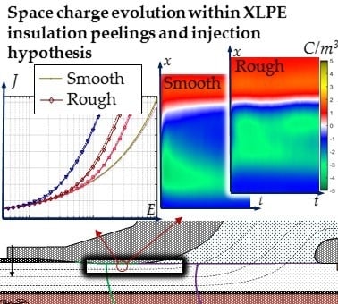
3.1. Roughness Enhanced Charge Injection

From the injection characteristics that are shown in Figure 5, a noticeable impact of the FEF distributions on the average injected charge densities, calculated with Equation (1), can be observed. For Schottky injection, the remolded surface had little to no impact on injection current densities compared to an ideal surface [3]. The remolded surface also shows only a linear dependency with electric field in the Schottky plot (B). The other surface types show higher charge injection above a certain field threshold, being distinguished by two distinct linear regions in the Schottky plot (B). Below the field threshold, all of the surface types show identical field dependency as the original Schottky current. Above the field threshold, rougher surfaces show a higher field dependency in the injection rate.
To model the impact of surface roughness (and local field enhancement) on charge injection, as observed in Figure 5B, the Schottky injection is modified, by altering its field dependency:
J s = λ R A 0 T 2 e ϕ B k T ( e e k T ( e E 4 π ε 0 ε r ) + e e k T ( e β S E 4 π ε 0 ε r Δ ϕ s ) ) .
here, βs is a unitless introduced field parameter and Δ ϕ s is an increased barrier height in eV necessary to adjust the high field behavior. In Equation (7), the first term in the sum is the original Schottky term, whereas the second one describes the increased charge injection due to interfacial roughness. The original Schottky current dominates at low fields, while at high fields the field dependency is defined by the βs parameter. The calculated results from Equation (7) are plotted with dotted lines in Figure 5A,B. As seen, the current densities match the results from Equation (1) for each type of surface. Table 1 shows the values for parameters βs. One can observe that they correlate with the maximal field enhancement and, thereby, the degree of surface roughness (Sa and Sdq). Additionally, barrier height modification Δφs, is the same for all surface types, with a value of 0.27 eV.
In Figure 5C, the impact on Fowler-Nordheim injection alone is shown, where the rough surfaces increase the tunneling rate by many decades. For the total current shown in Figure 5D, considered to be the sum of both Schottky and Fowler–Nordheim injection, this creates a surface type dependent tunneling onset field. To simulate this tunneling behavior, the original tunneling equation (here without the impact of temperature and the image charge effect for simplicity) is modified by introducing field parameter βFN:
J F N = e 3 ( β F N E ) 2 8 π h ϕ F N e ( 4 3 ( 2 m ħ 2 ) ϕ F N 3 2 e ( β F N E ) ) .
When tuning the unitless beta parameters βFN in the expression for Fowler–Nordheim injection, the same set of field parameters as for Schottky injection is obtained (e.g., βs = βFN), as shown in Table 1. As the unmodified Equation (8) was used, neglecting the image charge effect, as in Equation (3), the β-parameters were selected to closely match in the range of the current density (10−17–10−7 A/m2) giving a poorer fit outside of this region, as displayed in Figure 5C (bottom left). For the remolded surface, a beta parameter of 1.3 was found to give the best fit to the averaged injection current density. This was slightly higher than the field enhancement, as the rates that were calculated with Equation (8) do not account for temperature and image charge effect, which are included in Equation (4).
For both Schottky and Fowler–Nordheim injection currents, the roughness enhanced charge injection estimated by including the local Laplacian field distribution can be fitted with the modified expressions using identical values of their field controlling parameters that are shown in Table 1. These field parameters also tend to correlate with the maximal field enhancement at surface asperities, which is expected, as there is strong non-linearity in Equations (2) and (3). This strong non-linearity, leads to most of the charge being supplied from a small surface fraction, at which the divergent interface field is enhanced the most by the rough geometry. This description of injection behavior does not take into account the impact of locally distributed charge density on the field distribution at the surface [6].
These roughness-modified charge injection equations can be further introduced into a one-dimensional bipolar charge model. The barrier heights, φB, φFN, as well as other parameters can now be changed without having to recalculate the local currents and averaging them.

3.2. Space Charge Measurement

In the previous section, modified injection behavior was calculated that could arise from using rough surface geometry. The anticipated behavior is that; little to no impact should be found at low field levels, whereas, above a certain threshold field, higher surface roughness should result in increased charge injection. Thus, this threshold field magnitude is expected to correlate with sample types in the hollowing order; Rough abraded < Abraded < Smooth abraded < backside (< remolded). For the smooth backside and remolded surfaces, no impact on injection rate is predicted below 100 kV/mm and could therefore be used as references. The tunneling behavior occurring at low field levels with rough surfaces as compared to smoother surfaces, can additionally give rise to charge packets in the material [12].

3.2.1. Impact of Sample Orientation and Polarity

In Figure 6, four different PEA measurements are displayed, which were obtained by using the same electrodes and only modifying the voltage polarity and sample orientation. In the figures, any charge exceeding 3 C/m3 is placed out of the colormap range, as they correspond to charges at the electrodes during polarization. Depolarization durations of around 18 h are shown.
At medium field strengths (34–39 kV/mm), more charge seems to be injected from the abraded surfaces than from the backside surfaces, regardless of the polarity, as observed in Figure 6. This could be related to the enhanced Schottky injection due to the increased roughness of the abraded surface, as described in the previous chapter. By comparing Figure 6A and Figure 6D, as well as Figure 6B with Figure 6C, similar charge distributions should be obtained as both sample orientation and polarity are reversed. This is true, although some deviation is observed that can be related to the thickness differences. In addition to these observations, fast charge buildup during polarization can be noticed with the stabilization over time after establishment. Furthermore, slow charge decay is observed during depolarization. From Figure 6, it seems that negative charge carriers exhibit lower injection and transport (detrapping and/or hopping transport) barriers than positive carriers. This effect could be attributed to semi-crystalline structure within the material, as the crystalline and amorphous phases are known to favour, respectively, hole and electron transport [11,13].

3.2.2. Impact of Poling Field Strength

PEA measurements were carried out at different poling voltages to investigate the increase of charge injection with electric field in XLPE with different degrees of surface roughness. The results are shown in Figure 7 for rough abraded, abraded, and backside surfaces types used as anodes, while all cathodes featured a backside surface type. Note that only the polarization sequence is shown with the gaussian peak removal, allowing here for a better comparison.
It is observed in Figure 7 that charge density increases with poling field and negative charge dominates at high field strength. Small deviations in sample’s thicknesses led to some variations in the mean poling field, as indicated above each plot in Figure 7. While larger increase in charge density is seen for the rougher surface types, the positive charge injected from these surfaces does not exceed the negative charge density from the smooth anode. It can be due to the morphology of the polymer favoring injection and transport for negative charge. When a higher positive charge is injected from rough anodes, it simultaneously increases the field level at the cathode and, therefore, both positive and negative charge density increase is observed. The net and mean charge densities calculated with Equations (5) and (6) are displayed as functions of the poling field in Figure 8. Additional measurements that are not shown in Figure 7 are also included in Figure 8.
The net charge density decreases for most samples with the poling electric field, which could be an effect related to the sample morphology, as seen in Figure 8 [11,13]. Data for remolded samples deviate from anticipated behavior, which predicts low injection rates. At an electric field higher than 45 kV/mm, higher charge density is observed in the remolded sample, which deviates from the reference. Such deviation could originate from either the higher sample thickness (700 μm) of this specific sample, or its manufacturing method, where the surface layer’s crystalline structure could be affected [5]. The depolarization curves in Figure 8B also show that, at high electric field, some charge has already disappeared between the end of the polarization (markers) and the start of the depolarization (solid lines) stage (note that ~5 minutes were required for resetting the system). For rough abraded, abraded, and smooth abraded surfaces, higher mean charge densities were measured as compared with those obtained for backside surfaces, as can be seen in Figure 8B. This fact might indicate electric field thresholds at approximately 30, 36, and 44 kV/mm, respectively, which can be related to the electric field thresholds in the Schottky injection described in Section 3.1.
High field behavior has been further evaluated in both polarization and depolarization sequences. Figure 9 shows the results of these measurements.
Charge packet-like behavior can be observed at high fields that may originate from a strong field dependency in the injection rate, or to the onset of tunneling [12]. This mechanism might provide a sudden large quantity of injected charge when the electric field at an electrode is increased. Such packets can propagate and cause field enhancement upon arrival at the opposite electrode, triggering a new packet of opposite charge. While the results that are observed in Figure 9 cannot indisputably reveal the nature of the injection type, it clearly shows that strong field dependency exists in the injection rate from these surface types. Additionally, it is observed that the charge decay during depolarization initially proceeds at a fast pace, but after 3–4 hours it slows down significantly. This effect could be explained by considering the ratio between the mobile charges (trapped in shallow and inter-level traps) versus deeply trapped charge, here referred to as the mobile charge ratio. A strong poling field could lead to a high mobile charge ratio, causing a fast-initial decay of the mobile charges, while, after some hours, mostly deeply trapped charge remains. Poling at medium (as observed in Figure 6) or low fields could lead to a much lower mobile charge ratio, and the same fast initial decay is therefore not observed. This effect shows that deep trapping and detrapping mechanisms exhibit a field dependency. Finally, the higher charge densities appearing at rough surfaces at high fields are also visible near the anodes in the depolarization sequence.

3.2.3. Impact of Temperature

Figure 10 shows the impact of temperature on charge accumulation is also studied. The results of PEA measurements performed at 50 °C and 70 °C for abraded and backside anodes.
Figure 10 illustrates an impact of temperature on the decay rate; the decay rate is higher at higher temperatures, regardless off the electrode type. While thermally activated detrapping can explain the observed behavior [14,15], increased Schottky injection of opposite charge may also occur. When electric field at the anode or cathode is reversed during depolarization (due to the remaining charge in the material), an opposite charge can be injected and transported into the material, decreasing the observed charge density with time. In Figure 10B, the decay rate close to the anode is faster than in the bulk of the material, which might be attributed to such an injection mechanism.
The net and mean charge densities calculated using Equations (4) and (5) are plotted as functions of temperature in Figure 11 (note that the applied voltage and its polarity was the same).
Some of the variations of charge quantities in Figure 11 can be explained by deviations in sample thickness and, thereby, mean poling field. For most of the samples, the field magnitudes were quite close and varied in the range from 30 kV/mm to 39 kV/mm. However, for some cases, a lower applied electric field of around 26 kV/mm occurred and resulted in a lower charge density, as observed for smooth abraded and backside samples at 50 °C. Additionally, a higher electric field of around 43 kV/mm applied to the smooth abraded sample at 70 °C induced somewhat higher charge density. Possible charge densities in the case of non-deviating poling fields are indicated with the arrows in Figure 11B for these measurements. High mean charge density was also observed for the rough abraded sample at 50 °C, but this deviation might instead originate from enhanced charge injection occurred for this surface type. The depolarization curves that are shown in Figure 11B also show that some charge is lost during time between the end of the polarization (markers) and the start of the depolarization (solid lines), which made calibration more demanding. The depolarization curves also show a similar increase in the charge decay rate with temperature for all samples.
The impact of temperature on the mean charge accumulation is rather weak. As both charge injection and charge transport rates are increased with temperature, similar charge accumulation is observed at high temperatures. Thermally activated detrapping should result in an increased mobile to trapped charge ratio, increasing the mobility/transport rate and charge decay rate during depolarization.

4. Discussion

4.1. Roughness Enhanced Charge Injection

The measurements revealed the appearance of electric field thresholds and stronger charge accumulation at rougher surfaces. However, the high field behavior is not as strong as anticipated from Equation (7) for Schottky injection rates.
Thus, at low electric fields (<25 kV/mm), different surface types show similar mean charge densities, with deviations of around 0.4 C/m3, as shown in Figure 8B. The model also predicts similar charge densities with different surface types, as the injection rates should be unaffected by roughness at low electric fields.
At high electric fields (>40 kV/mm), the observed injection rates from rough abraded anode surfaces are comparable to the injection rates from smoother cathodes, as can be seen in Figure 7. Even though negative injection rate is favored due to sample morphology, the positive charge accumulation that is observed in the experiment seems to be much lower than what is anticipated from the injection equations. The value of the β-parameter (β = 13 for the rough abraded surface), estimated from the Laplacian field calculation, can thus be overestimated. However, the FEF histogram, as shown in Figure 3B, can be narrowed when field dependent charge transport is considered, as reported in [6,7]. A strong field dependency in the transport rate will reduce the field at high field regions and redistribute it towards weak-field regions [6,7]. This effect will, in turn, reduce the β-parameters at high fields, still anticipating increased charge injection for rougher surfaces, but at lower amounts possibly matching the experimental data.
At high fields, charge packets in the material samples with typical propagation times in order of several hours are observed, as reported in [6,7]. Such packets could indicate Fowler–Nordheim injection (tunneling) or a strong field dependency in the injection rate [12]. Including Fowler–Nordheim injection in a one-dimensional model should however result in a very high charge density adjacent to the injecting electrode, which has not been observed in the measurement. However, it is still possible that a small fraction of the surface (the rough asperities) is supplying tunneling current at high fields, but further transport is limited by adjacent localized charge accumulation due to a local mobility (or conductivity) gradients [6].

4.2. Overall Observations

While similar negative and positive charge densities are present at low fields, more negative charges are observed at higher poling field levels, as seen in Figure 8. One might also notice that the net charge density in Figure 11A does not change significantly with temperature. This behavior can be related to lower injection, transport, and detrapping barriers for electrons than for holes in the material, which, in turn, might originate from the structure of the polymer. Thus, in semi-crystalline regions, electrons are favorably transported in between polymer chains in the amorphous phase [16]. As the processing steps affect the morphology of the cable peelings used (extrusion, vulcanization, and degassing), a high fraction of amorphous regions may exist in the material, due to crosslinking [17] or processing itself. It is also possible that crystallinity in the used DC grade XLPE is suppressed at both low and elevated temperatures, as crystal growth can be inhibited by polymer cross-links in the material [17]. These factors could explain the favorable conditions for electron transport and injection in the HVDC cable peelings. Interestingly, the behavior is opposite to what is observed in press-molded LDPE plates, where higher positive charges are generally recorded [15,18].
The here reported space charge accumulation shows comparable behavior to previous results reported in [7], where the same cable peeling was used at different increasing electric field levels. However, when not using virgin samples under each new electric field, some trapped homo charge remains in the samples, which reduced the transients at higher stress in [7].
The charge decay rates during depolarization show a high temperature dependency. This could be related to higher charge mobility, a higher detrapping rate, and possibly also to slightly higher opposite charge injection. In previous work [7], the impact of temperature on the injection rate with rough surfaces was studied. It was found that temperature affected the base level and not the field dependency in the Schottky injection. The described injection equations (Equation (7) and Equation (8) and the parameters in Table 1) should thus also be viable at elevated temperatures, given that the base level (for Schottky injection; λRA0) and energetic barriers φB, φFN are properly tuned.

5. Conclusions

The presented results demonstrate that control over micro-scale interfacial geometry is a necessity in on-site manufactured HVDC cable accessories, since surface roughness leads to enhanced charge injection into the insulation. By reducing surface roughness, high charge accumulation can be prevented in HVDC cable insulation.
Two charge injection hypotheses, which predict higher charge accumulation from rough surfaces above a certain electric field threshold, have been experimentally examined and revealed. However, exact local interfacial charge injection and accumulation is likely more complex than here-assumed Laplacian surface field impact. Nevertheless, these charge injection hypotheses can be used to anticipate the overall charging behavior of smooth and rough interfaces at low to medium electric field strengths.
A series of field and temperature dependent effects have been observed, affecting injection and charge accumulation in the material. These effects are to be incorporated in a bipolar charge injection and transport model, which is outlined in part II of this article and compared against the experimental results.

Author Contributions

R.G. carried out PEA measurements and supplied base level coding for signal processing. E.D. further developed the coding and processed the PEA results. He additionally developed the injection hypothesis and prepared the manuscript. E.M.J. and Y.V.S. supervised the work. All authors have read and agreed to the published version of the manuscript.

Funding

This work was funded by Nexans Norway AS within the framework of the industrial PhD project carried out by Espen Doedens.

Acknowledgments

For financial support Nexans Norway AS is acknowledged while Chalmers is acknowledged for their supply of expertise and supervision. The Nexans Research Centre (NRC) of Lyon is also acknowledged for supporting and facilitating the PEA measurements carried out by Raphaël Guffond. A special acknowledgement goes out to Christian Frohne for his mentorship and support during the work. Additionally, the authors’ colleagues are acknowledged for their support, contributing to the realization of this work.

Conflicts of Interest

The authors declare no conflict of interest.

References

  1. Tanaka, T. Space charge injected via interfaces and tree initiation in polymers. IEEE Trans. Dielectr. Electr. Insul. 2001, 8, 733–743. [Google Scholar] [CrossRef]
  2. Morshuis, P. Interfaces: To be avoided or to be treasured? What do we think we know? In Proceedings of the IEEE International Conference on Solid Dielectrics (ICSD), Bologna, Italy, 30 June–4 July 2013; IEEE: Piscataway, NJ, USA, 2013; pp. 1–9. [Google Scholar] [CrossRef]
  3. Taleb, M.; Teyssedre, G.; Le Roy, S. Role of the interface on charge build-up in a low-density polyethylene: Surface roughness and nature of the electrode. In Proceedings of the IEEE Conference on Electrical Insulation and Dielectric Phenomena, Virginia Beach, VA, USA, 18–21 October 2009; IEEE: Piscataway, NJ, USA, 2009; pp. 112–115. [Google Scholar] [CrossRef]
  4. Novikov, S.V. Rough electrode surface: Effect on charge carrier injection and transport in organic devices. Macromol. Symp. 2004, 212, 191–200. [Google Scholar] [CrossRef]
  5. Doedens, E.H. Characterization of Different Interface Types for HVDC Extruded Cable Applications. Lic. Thesis, Chalmers University of Technology, Göteborg, Sweden, 2018. Available online: https://research.chalmers.se/publication/502706/file/502706_Fulltext.pdf (accessed on 6 April 2020).
  6. Doedens, E.; Jarvid, M.; Serdyuk, Y.V.; Guffond, R.; Charrier, D. Local Surface Field- and Charge Distributions and Their Impact on Breakdown Voltage for HVDC Cable Insulation. In Proceedings of the International Conference on Insulated Power Cables (Jicable), Cigré, Versailles, France, 23–27 June 2019. [Google Scholar]
  7. Doedens, E.; Jarvid, E.M.; Frohne, C.; Gubanski, S.M. Enhanced charge injection in rough HVDC extruded cable interfaces. IEEE Trans. Dielectr. Electr. Insul. 2019, 26, 1911–1918. [Google Scholar] [CrossRef]
  8. COMSOL Multiphysics® v.5.3. Available online: www.comsol.com (accessed on 16 April 2020).
  9. Doedens, E.; Jarvid, M.; Gubanski, S.; Frohne, C. Cable surface preparation: Chemical, physical and electrical characterization and impact on breakdown voltage. In Proceedings of the International Symposium on HVDC Cable Systems (Jicable-HVDC), Dunkirk, France, 20–22 November 2017. [Google Scholar]
  10. Good, R.H.; Müller, E.W. Field Emission. In Electron-Emission Gas Discharges I/Elektronen-Emission Gasentladungen, I. Encyclopedia of Physics/Handbuch der Physik; Springer: Berlin/Heidelberg, Germany, 1956; pp. 176–231. ISBN 978-3-642-45846-0. [Google Scholar]
  11. Guffond, R.; Combessis, A.; Hole, S. Contribution of polymer microstructure to space charge, dielectric properties and electrical conduction. In Proceedings of the 2016 IEEE Conference on Electrical Insulation and Dielectric Phenomena (CEIDP), Toronto, ON, Canada, 16–19 October 2016; IEEE: Piscataway, NJ, USA, 2016; pp. 141–144. [Google Scholar] [CrossRef]
  12. Baudoin, F.; Laurent, C.; Le Roy, S.; Teyssedre, G. Charge packets modeling in insulating polymers based on transport description. In Proceedings of the Annual Report Conference on Electrical Insulation and Dielectric Phenomena, Montreal, QC, Canada, 14–17 October 2012; IEEE: Piscataway, NJ, USA, 2012; pp. 665–668. [Google Scholar] [CrossRef]
  13. Moyassari, A.; Unge, M.; Hedenqvist, M.S.; Gedde, U.W.; Nilsson, F. First-principle simulations of electronic structure in semicrystalline polyethylene. J. Chem. Phys. 2017, 146, 204901. [Google Scholar] [CrossRef] [PubMed]
  14. Hoang, A.; Pallon, L.; Liu, D.; Serdyuk, Y.; Gubanski, S.; Gedde, U. Charge Transport in LDPE Nanocomposites Part I—Experimental Approach. Polymers 2016, 8, 87. [Google Scholar] [CrossRef] [PubMed] [Green Version]
  15. Hoang, A.T.; Serdyuk, Y.V.; Gubanski, S.M. Charge Transport in LDPE Nanocomposites Part II—Computational Approach. Polymers 2002, 8, 103. [Google Scholar] [CrossRef] [PubMed]
  16. Serra, S.; Tosatti, E.; Iarlori, S.; Scandolo, S.; Santoro, G.; Albertini, M. Interchain states and the negative electron affinity of polyethylene. In Proceedings of the 1998 Annual Report Conference on Electrical Insulation and Dielectric Phenomena (Cat. No.98CH36257), Atlanta, GA, USA, 25–28 October 1998; IEEE: Piscataway, NJ, USA, 1998; Volume 1, pp. 19–22. [Google Scholar] [CrossRef]
  17. Nilsson, S.; Hjertberg, T.; Smedberg, A. Structural effects on thermal properties and morphology in XLPE. Eur. Polym. J. 2010, 46, 1759–1769. [Google Scholar] [CrossRef]
  18. Boufayed, F.; Teyssèdre, G.; Laurent, C.; Le Roy, S.; Dissado, L.A.; Ségur, P.; Montanari, G.C. Models of bipolar charge transport in polyethylene. J. Appl. Phys. 2006, 100, 104–105. [Google Scholar] [CrossRef] [Green Version]
Figure 1. Schematic structure of a cable joint. Additional layers providing water blocking, mechanical strength, etc. are not shown. The physical interface studied in this work is indicated by the red circle. Note that for the sake of simplicity, the axisymmetric coordinates (r, ϕ, z) at the micro-scale are replaced by Cartesian coordinates (x, y, z). In addition, any interstitial material (grease, oil, etc.) is considered as a part of the electrode, owing the low conductivity in XLPE.
Energies 13 02005 g001
Figure 2. Sample preparation, storage and space charge measurements performed in the present study ((A), left). Previously performed work ((B), right) encompassing profilometry, field simulation and injection current estimation [5,6,7], allowing for the derivation of modified injection laws in the present study. A Cartesian coordinate system (x, y, z) is adopted, with estimated current density oriented here in the x-direction.
Energies 13 02005 g002
Figure 3. Local field enhancement in the interfacial region of an abraded surface (colormap shows FEF and streamlines show field orientation) ((A), left). Corresponding Field enhancement factor (FEF) histograms for the points positioned at the surface ((B), right). Different surface types with different degrees of surface roughness are shown, and the results are obtained from Laplacian field calculation. Surface fractions containing reduced field (FEF < 1) and increased field (FEF > 1) are indicated.
Energies 13 02005 g003
Figure 4. Illustration of the Pulsed-Electro-Acoustic (PEA) setup and the sample configuration. Also, measurement dimensions (x, t) are indicated.
Energies 13 02005 g004
Figure 5. Calculated injection characteristics at 25 °C (solid lines with markers) using the Laplacian field enhancement factors (FEF) distributions and fitted curves using Equation (7) and Equation (8) (dash-dotted lines). A 1.5 eV barrier height was used in the calculations. Schottky currents are shown in a double logarithmic plot ((A), top left) and a Schottky plot ((B), top right). Fowler–Nordheim injection ((C), bottom left) is displayed in a double logarithmic plot. The total current ((D), bottom right) corresponds to the sum of the Schottky and Folwer-Nordheim injection current densities.
Energies 13 02005 g005
Figure 6. PEA measurements showing impact of polarity and sample orientation. 15 kV of positive or negative poling voltage was used at 25 °C. polarity and orientation of the electrode types is indicated in the figures. In each figure, SC-# indicates sample identification number, followed by the mean field strength during poling and temperature. The mean field strength is defined as poling voltage divided by sample thickness (measured post-measurement). Data larger than +/− 3 C/m3 have been colored white in the colormap as the electrode peaks during polarization should be disregarded in the comparison.
Energies 13 02005 g006
Figure 7. PEA measurements at 25 °C, using different poling voltages, polarization sequence only. All samples feature the listed surface type as anode (top) and a backside cathode (bottom). The peaks positioned at the anode and cathode have been removed by gaussian peak removal. White regions correspond to charge densities beyond ±5 C/m3.
Energies 13 02005 g007
Figure 8. Impact of mean poling field at 25 °C on net charge density ((A), left) and mean charge density ((B), right). The indicated surface types are used as positive anode, while the cathode is a backside type surface in all experiments. The markers indicate the value in the end of the polarization. The solid lines in (B) show the mean charge density against time during depolarization. Dashed lines indicate trendlines. The pink shaded area in (B) indicates the trend for backside surfaces, which can be treated as reference.
Energies 13 02005 g008
Figure 9. PEA measurements at high electric fields (61–76 kV/mm), at 25 °C and using +30 kV poling voltage, showing space charge packet-like behavior and fast initial depolarization. With a rough abraded sample ((A), top left), an abraded sample ((B), top right), a smooth abraded sample ((C), bottom left) and a backside sample ((D), bottom right). Data larger than ±5 C/m3 has been colored white in the colormap.
Energies 13 02005 g009
Figure 10. PEA measurements performed at 50 °C (left, (A,C)) and 70 °C (right, (B,D)) with +15 kV of poling voltage. Top figures show measurements with abraded anode while bottom surfaces show measurements with a backside anode.
Energies 13 02005 g010
Figure 11. Impact of temperature at +15 kV poling, using different temperatures, on the net charge density ((A), left) and the mean charge density ((B), right). The indicated surface types were used as positive anode, while the cathode was a backside type surface in all experiments. Markers indicate the value in the end of the polarization. The solid lines in (B) show the mean charge density against time during depolarization. Dashed lines indicate trendlines. The arrows in (B) indicate probable corrections for thickness (poling field) deviations.
Energies 13 02005 g011
Table 1. Sa parameters, Sdq parameters, maximal field enhancement, and used field parameters for the different surface types.
Surface TypeA: Rough AbradedB: AbradedC: Smooth AbradedD: BacksideE: Remolded
Roughness, Sa 174.634.619.012.51
Roughness, Sdq 175.337.623.612.41
Max field enhancement, FEFmax 29641.81.1
Injection field parameter, βs, βFN 313 (9)6.54.31.91.3
1 The data is normalized against the remolded surface. 2 Average of the 100 highest FEF values from the histogram. 3 Parameters that best fitted the charge injection behavior in Figure 5. For rough abraded a lower value was later used in the simulations, displayed within the parenthesis.

