1. Introduction
Instrument transformers are widely used to decrease the value of the voltages and currents from the power grid to the levels appropriate for measuring and to protect circuits. Most of them are inductive and the non-linearity of the magnetization curve of their magnetic core causes the need for testing their transformation accuracy in the full range of the primary current/voltage [
1,
2,
3]. Due to the large number of non-linear devices, the quality of the electrical energy in the power networks is deteriorated and thus the signal transformed by the instrument transformers is distorted. In the case of inductive current transformers this may even have a negative impact on their transformation accuracy of the main component of the distorted current [
2]. Of course, ratio and phase errors in the transformation of higher harmonics are usually different than determined for sinusoidal signals [
3,
4,
5,
6,
7,
8,
9]. However, the 0.1 and 0.2 accuracy classes of inductive current transformers designed for transformation of sinusoidal currents of frequency 50 Hz may be preserved to 5 kHz [
7]. In the case of the inductive voltage transformers designed for transformation of sinusoidal voltages, their frequency range of operation without resonance for higher harmonics is dependent on the rms value of the primary voltage [
6]. Therefore, to determine the measurement error of non-sinusoidal electrical power and energy caused by instrument transformers, the wideband testing of their accuracy is necessary [
10,
11,
12]. However, there are no specific requirements or evaluation methods for assessing the transformation errors of the distorted signals by the inductive current and voltage transformers. Existing standards concern the low-power instrument transformers [
13,
14,
15]. It is specified that to “provide a realistic image of the dynamic requirements of the transformer”, the accuracy of such devices should be tested with a signal containing both 50 Hz (main) and higher harmonic components. However, “for practical considerations, it is accepted that the accuracy tests be made with only one single harmonic frequency applied at the primary side for each measurement” [
13]. In the case of an inductive instrument transformer, such a solution is unacceptable. Therefore, a proper wideband programmable power source capable of generating the voltage of the required rms value with both main and higher harmonics is essential. Moreover, the wideband step-up current (or voltage) transformer is used [
8,
9,
16,
17].
A typical programmable power supply is able to generate voltage that consists of basic and some percentage of higher harmonics. Their rms values are internally limited. However, some power sources may be controlled by an external reference voltage. Due to the inductive reactance of the step-up current transformer and its current track, the main problem arises from the requirement to maintain the rms value of the higher harmonic of the distorted output current with the increase in its frequency. This causes the need to increase the rms value of the higher harmonic of the output voltage. The limiting values for such operating conditions for the power source result from the maximum values of its output voltage, current and active/reactive power, as well as its slew rate. There are two main types of output stages in wideband power sources: a pulse width modulated (PWM) inverter and linear amplifiers. A PWM drive switches the voltage across the transistors on and off at a very high frequency (e.g., 20 kHz); it controls the width of the pulses and the average voltage supplied to the output. In the linear amplifiers. transistors in linear mode are used to create an output voltage that is as accurate as possible in reflecting the input voltage but with significant gain of power.
In this paper, a comparison of the wideband power sources of a PWM inverter with the power supply composed of an audio power amplifier and a two-channel arbitrary generator is discussed. Their application is to supply a step-up current transformer for the generation of a distorted current required to test the transformation accuracy of the distorted currents of the inductive current transformers. Therefore, the wideband generation capabilities of both the power sources were tested in order to indicate the most favorable for such utilization. The calculation method to determine the maximum rms values of the higher harmonic of the distorted current for its required main harmonic component is presented Moreover, the proposed equations also enables a determination of the maximum rms values of the main harmonic of the distorted current for which the required higher harmonic component may be obtained. Therefore, three limitations are defined: voltage, current and slew rate. Moreover, in order to increase the output current of the power source for the inductive loads, the compensation method of such reactance for both the main and higher harmonic is developed.
2. Tested Wideband Power Sources
The PWM-based wideband power source consists of four main elements: an input stage with active PFC (Power Factor Correction), a DC rail, a control circuit and an output-stage PWM inverter. The control of the PFC is provided by the MOSFET drive that controls the rectified current through the inductor in order to ensure a proportional input current to the AC line voltage. In
Figure 1 the simplified block diagram of the PWM-based arbitrary waveform power source with the boost converter-based PFC is presented [
18,
19].
In solutions with the boost converter-based PFC, the output voltage may be higher than the supplying voltage of the power source. It works by storing energy in the inductor L of the DC rail when the transistor Q is ON. During this time, the energy required by the load is supplied by the output capacitor Co. When the transistor Q switches OFF, polarity of the voltage across the inductor reverses causing diode D to become forward-biased and energy is transferred to the capacitor C
0. Therefore, pure capacitive loads may not be supplied by the device. A PWM-controlled inverter is responsible for generating the required waveform, as a series of various-width rectangles. Such an inverter consists of two transistors, where one is responsible for generating the upper part of the waveform (voltage values from 0 to +U
max) while the other for the lower part (voltage values from −U
max to 0). The control pulses are generated by comparison of the carrier triangle wave with the desired reference signal. The upper transistor is switched on when the reference signal value is higher than the carrier one and switched off when the value is lower. The control signal for the second transistor is inverted [
19]. The tested PWM-based power source’s rated apparent power is equal to 2 kVA. It is able to operate in two voltage ranges: 0–150 V and 0–300 V, with the maximum rms values of the output current equal to 16 A or 8 A, respectively. Its frequency band of operation with the rated apparent power is equal to 1 kHz. It is designed for the generation of voltages with higher harmonics of frequencies up to 2400 Hz, with a limited rms value of 20% of the main component of the distorted output voltage. This range can be increased during operation as a reference signal amplifier.
In a linear amplifier, such as an audio power amplifier, the transistor in its output stage typically operate in class AB since class A is less efficient. They are working on a push-pull topology, with one transistor responsible for the positive part of the signal and the other for the negative. Since each transistor is conducting for more than half of the period, the crossover distortion is reduced. The H class amplifiers have the same working principle, but are powered by a lowering converter, thereby keeping the input voltage slightly higher than the output voltage that increases the device’s efficiency. Audio amplifiers usually have two channels that can either work separately or be bridged, which is a useful feature as it allows to double the output voltage. Common control for gain will automatically track each channel identically and the input voltage of the first channel will be amplified in the counter-phase by each channel. There are three main protection systems of such devices. The overdrive protection limits the maximum value of the output voltage; it is commonly made by a Zener diode connected at the output of the power stage. The output current limitation and the power protection are usually joined together as overheat protection with a bimetallic strip on the radiators of the output transistors. During this research study, two different types of audio amplifiers were tested. The rated output power of both these units were in accordance with the data provided by their manufactures, which is 2 kW available in 2 Ω per channel and 4 kW in 4 Ω for the bridge mode. The typical output voltage of a single channel is equal to 70 V rms while when bridged it increases to 140 V rms. The expected output currents are equal to 28 A rms. The application of a linear amplifier to supply the step-up current transformer for the generation of a distorted current to test the transformation accuracy of an inductive current transformer requires a reference voltage source from an arbitrary generator. Its main components are the Digital Signal Processor (DSP), A/D converter and RAM memory. The desired waveform is mathematically modeled and sampled in the time dimension, while the number of samples is dependent on the DSP’s clock frequency. The values for one time period are than stored in RAM memory. When the generation begins, for every clock signal the required value from the RAM memory is read and sent to the D/A converter. The amplitude of the generated waveform is adjusted by a programmable gain amplifier at the output of a D/A converter [
20]. A summary of the specifications of both power sources in order to facilitate the comparison is presented in
Table 1.
3. Factors Determining the rms Value of the Higher Harmonic of the Distorted Output Current of the Wideband Power Sources
The first limitation is the maximum peak-to-peak output voltage of the power source; it is most important for inductive loads and depends on the insulation system and the maximum collector–emitter voltage of the transistors used in the output stage. If a distorted voltage is a sum of two sinusoidal voltages, one of the base frequency and the other with multiples of this frequency (its higher harmonic), it can be calculated from Equation (1):
where U
max.pp—the maximum value of the peak-to-peak distorted output voltage of the power source; U
h1—the rms value of the main component; C—Crest factor; and U
hi—the rms values of the
hi higher harmonic of multiple frequency of the main component of the distorted voltage.
The second limitation is the rated rms value of the output current of the power source. Therefore, the maximum rms value of the higher harmonic of the distorted output current is equal to
where I
max—rated rms value of the output current of the power source; I
h1—required rms value of the main component; and I
hi(I
max)—the maximum rms value of the
hi higher harmonic.
The third limitation is the rms value of the maximum output apparent power of the power source. Its value is restricted by the maximum value of the active power dissipation of the used transistors and the efficiency of their cooling system.
where S
max—the maximum value of the apparent power; and U
max—rated rms value of the output voltage.
The last limitation of the frequency range for the operation of the wideband power sources is a dependence on the slew rate of the output transistors. This parameter describes the speed at which the output voltage may be switched between its maximum and minimum values. If the switching speed is too low, the output voltage is not able to reach its required level within the available time, resulting from the frequency and the output signal not corresponding to the input signal. In order to maintain a proper quality of the output signal, either value of the voltage or frequency must be decreased. Slew rate is not usually given in the technical specification of the power source, but it can be estimated from the maximum rms value and frequency of the output voltage:
where f
hi—frequency of the
hi higher harmonic ought to be generated; and f
max—maximum frequency of the output voltage of the power source.
In order to evaluate the usefulness of the device for supplying the wideband CT testing circuits, it is necessary to determine from Equation (5) the maximum possibility to obtain an rms value of the highest frequency harmonic for the required output current.
The maximum power limitation is not important since it results from output current and voltage. After transformation of Equation (1), considering any type of load the maximum rms value of the higher harmonic of the output current resulting from the maximum peak-to-peak output voltage of the power source may be calculated from Equation (6):
where R—resistance of the load; L—inductance of the load; and f
h1—frequency of the main harmonic of the output voltage.
After transformation of Equation (4), for inductive load the maximum rms value of the higher harmonic of the output current resulting from the slew rate of the output voltage may be calculated from Equation (7):
The maximum rms values of the output voltage, current and frequency, as well as the inductance of the load are required in order to determine the maximum rms values of the higher harmonics of the output current. Such parameters are easily accessible in the data sheet of the power source or the audio amplifier.
The generation ability of the power source also depends on the required rms value of the main harmonic of the distorted output current. The results presented in
Figure 1 are determined for 6.5 A rms. In the case of small inductive loads, such as 5 mH, the frequency band of their operation results from current and frequency limitations (
Figure 1).
In
Figure 2 the following notations are used: U
SRhi—the limitation resulting from the maximum frequency of the output voltage of the power source; U
max—the limitation resulting from the maximum peak-to-peak output voltage; I
max—the limitation resulting from the maximum rms values of the output current; and Band—resultant frequency band of operation of the power source for a given rms value of the main harmonic of this distorted current equal to 6.5 A with a load inductance equal to 5 mH.
An increase in the load’s impedance from 5 mH to 10 mH will result in a rise in the voltage limitation as a determining factor of the frequency band of the power source’s operation; it also still results from the current and frequency limitations (
Figure 3).
A low required rms value of the basic harmonic of the distorted output current causes a decrease in the current limitations. The frequency limitation remains the same. The voltage limitations for both cases are indistinguishable. It is due to the fact that the load’s inductance is relatively low (10 mH). Therefore, the reactance is equal to 3.14 Ω for the main component; thus, a change in its current by 1.5 A will result in the voltage available for the higher harmonic being lowered by less than 5 V. Such a value is negligible in relation to the level of voltage required for generation of the higher harmonics of a distorted current.
The maximum rms values of the main harmonic of the distorted current for which the required percentage value of the higher harmonic of a given frequency may be obtained, result from three previously described limitations in accordance with the following equations:
where f
h1—frequency of the main harmonic of distorted current ought to be generated.
where RR%—required percentage value of the higher harmonic of a given frequency in the distorted current.
The calculated maximum rms values of the main harmonic of the distorted current for which a higher harmonic of a given frequency may be equal to its 10% level for the PWM power source (2 kVA\150 V\16 A) and the power supply composed of the audio power amplifier (4 kW\140 V\28 A) are presented in
Figure 4.
The slew rate limitation resulting from the maximum frequency of the output voltage of the PWM power source equal to 1 kHz is lower than for the audio amplifier. Therefore, the main harmonic of the distorted current for which a higher harmonic of a given frequency may be equal to its 10% level may be ensured in the smaller range of frequencies of the higher harmonics.
4. The Maximum rms Values of the Output Current and Voltage for a Sinusoidal Input Voltage of Frequency 50 Hz
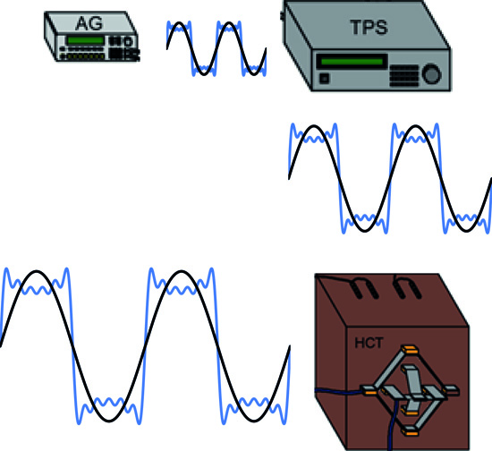
In the first stage of the laboratory studies, the parameters declared by the manufacturer of the PWM-based power source were verified, confirming the availability of 2 kVA of apparent power and an rms value of the sinusoidal output current of a frequency of 50 Hz equal to 16 A (150 V)\8 A (300 V). Various types of loads were used, including pure resistive\inductive and their parallel and serial connections. During the tests of the 2 kW\4 kW audio power amplifier for its given load the input voltage was slowly increased until one of the protection systems of the power source was activated. Then its value was decreased to ensure its steady state operation for at least 5 min. If the protection system was again activated, the procedure was repeated for the lower rms value of the input voltage. The measuring circuit is presented in
Figure 5.
In
Figure 5 the following notations are used: AG—arbitrary waveform generator; PA—preamplifier with insulation transformers; TPS—tested power source; DPM—digital power meter; I
nR—adjustable inductor; and R
nR—adjustable resistor.
The two-channel DSP-based arbitrary waveform generator was the source of the input voltage for the tested linear amplifiers and the PWM-based wideband power source operating as the amplifier. Its first channel is used for generation of a 50 Hz frequency basic harmonic component of the distorted input voltage, while the second one is used for generation of the higher frequency harmonic. In order to obtain the distorted voltage composed of two harmonics, the signals from both channels must be added together. Therefore, serial connection of two voltage sources is required. However, direct connection of two channels of the arbitrary waveform generator was not used since it caused load between the channels. Moreover, to avoid over-voltages during the regulation of their rms values, each channel was connected through the preamplifier with a continuous regulation of the output voltage and a separate insulation transformer. The output current, voltage and active\reactive power of the tested power sources were measured through the first channel of the digital power meter. Its second channel was used to measure the same quantities at the load.
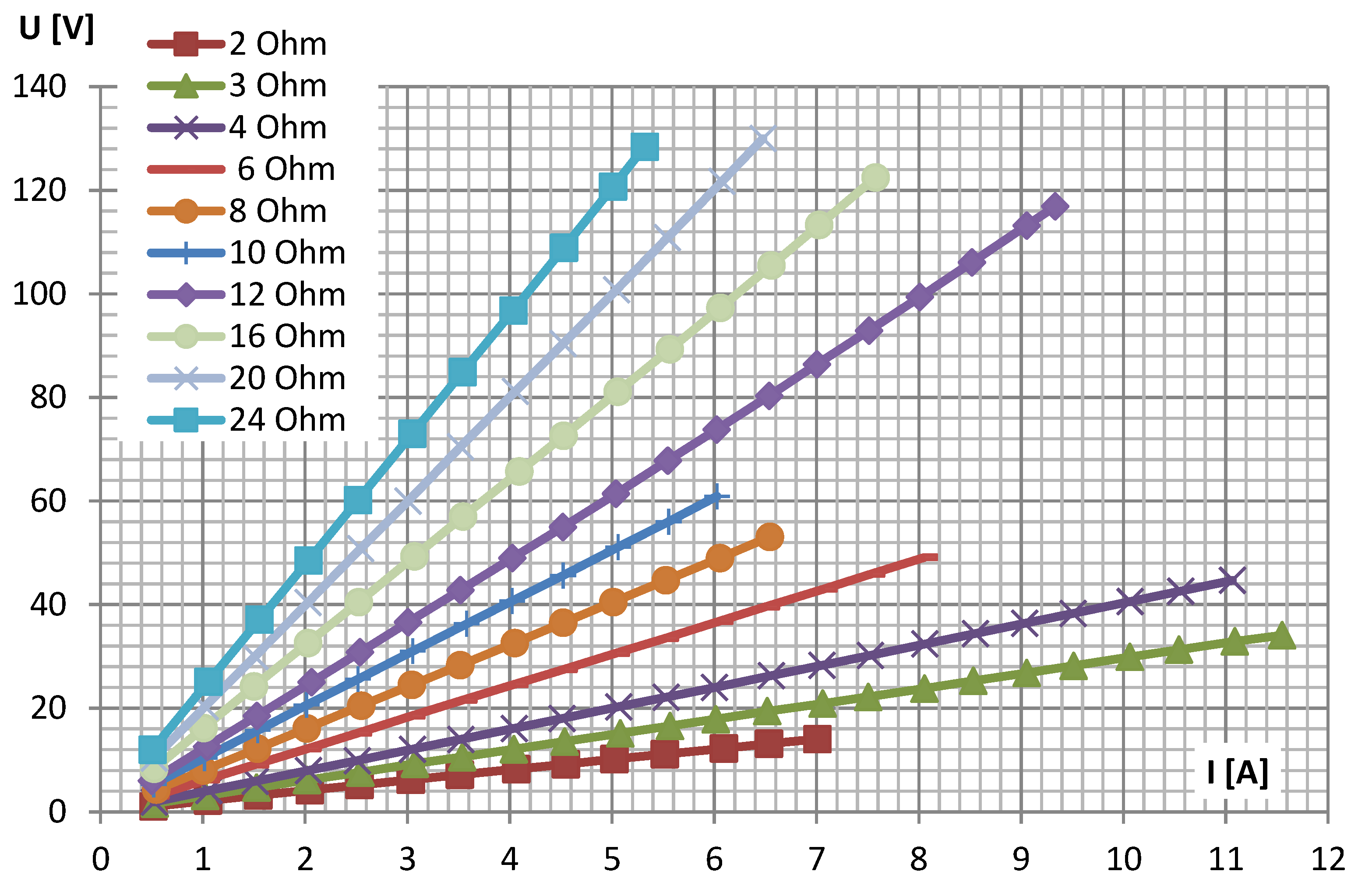
In
Figure 6 the rms values of the output current vs. output voltage of the audio power amplifier for resistive and inductive loads for single channel operation and in bridged mode are presented. The values of the resistance and inductive reactance were changed during the tests starting from 2 Ω (single-channel mode) to 4 Ω (bridged mode) and up to 80 Ω.
During the test for each resistance/reactance of the load, the value output current was increased from 0 A with a 0.5 A step and kept steady for 5 min to ensure a steady operation of the amplifier. Such a sequence was repeated until the protection system was triggered. The output current was limited to a 24 A single channel instead of 28 A as declared by the manufacturer, and the output voltage was limited to 120 V in bridged mode instead of 140 V. The difference between the measured results and theoretical for the 2 Ω load is a result of the resistance increase caused by the thermal effect of the current flowing through the resistor. The maximum achievable active power of the device was lower than that declared by the manufacturer. It is below 1.7 kW instead of 2 kW for single channel into 2 Ω and below 3.7 kW instead of 4 kW into 4 Ω for the bridged mode. The maximum output reactive power for the inductive loads is equal to 0.7 kVA for single channel into 6 Ω and 1.2 kVA for the bridged mode into 12 Ω. The difference in output power among the different load types is a result of a phase shift between the voltage and current on the inductive loads. While working on a resistive load, the maximum output current is in phase with the maximum output voltage—the transistor is polarized towards conduction. If the load is purely inductive, the maximum current is obtained when the output voltage reaches 0, but at this moment the transistor should be reaching reverse polarization. If the current value is too high the voltage drops and the internal resistances of the amplifier are too high and interrupts the proper polarization of the output transistors; this leads to unstable functioning of the device.
To increase the available reactive output power and rms value of the current, an adjustable resistor was additionally connected serially to the inductive load (
Figure 7).
In
Figure 7, the notation 2R + 2L refers to a series connection of resistance 2 Ω, with an inductive reactance 2 Ω, and 1R + 2L a series connection of resistance 1 Ω, with an inductive reactance 2 Ω, etc.
The results show that to obtain an apparent output power for the inductive load that is equal to the active power generated for a purely resistive load, it is necessary to connect, in series, a resistor whose resistance is equal to the reactance of the load. Therefore, the power factor of the load must be over 0.7.
The 50 Hz performance tests also allows to detect malfunction in the design of the audio amplifier. In
Figure 8 the results of the tests for another 2 kW\4 kW audio amplifier are presented.
In the tested audio amplifier, a common cooling system for both channels was used. Therefore, it was unable to generate the rated output power even for a 50 Hz sinusoidal output current and voltage of the resistive load. This causes a decrease in the output current for loads from 6 Ω to 10 Ω.
5. Application of Tested Wideband Power Sources
In the presented application, the tested wideband power source was used for generation of a distorted current for supplying the step-up current transformer required for testing the inductive current transformer’s accuracy in transforming the harmonics [
7,
17]. Therefore, laboratory tests were performed in order to determine their frequency band of operation and the required rms values of the main and higher harmonics of the distorted output current of the step-up current transformer. Moreover, the compensation system to decrease the rms value of the required output voltage for the inductive load was implemented. The measuring circuit is presented in
Figure 9.
In
Figure 9 the following new notations are used: L
nf—compensation inductor for 50 Hz component; C
C1—compensation capacitors for 50 Hz component; C
Ch—switchable capacitor for compensation of higher harmonics; CT—current transformer; and HCT—step-up current transformer. The frequency band of the HCT operation is reported in [
17]. The transformation accuracy of the CT, similar to the one used in this measuring system, is analyzed in [
7].
The output current, voltage and active\reactive power of the tested power source were measured through the first channel of the digital power meter. Its second channel was used to measure the same quantities at the supplied step-up current transformer. The inductance of the step-up current transformer and its current track were compensated for main and each higher harmonics. The higher harmonic compensator consists of a series of switchable capacitors that enables the adjustment of the resultant capacitance to the specific frequency of the required higher harmonic in the output current. The compensation is required to decrease the needed rms value of the higher harmonic of the output voltage to obtain the required rms value of the output current. The capacitance is too small to conduct the basic 50 Hz component of the distorted output current. Therefore, in parallel to the higher harmonic compensation, a capacitor in series with inductance were connected. They are adjusted to produce a short circuit for a 50 Hz component. During the tests to determine the power source’s frequency band of operation, the required rms values of the higher harmonic of the distorted output current of the step-up current transformer was equal to 10% of the main harmonic. Its frequency was slowly increased by 50 Hz until one of the protection systems of the power source was activated. Then its value was decreased to ensure a steady state operation for at least 5 min. If the protection system was again activated during this period, the procedure was repeated for the lower value of the frequency of the higher harmonic. The object of the test is to achieve the highest possible rms value of the distorted output current of the step-up current transformer with the rms values of the higher harmonics equal to 10% of its main component.
During the tests, the frequency band of operation of the PWM-based power source for a required rms value of its main component were determined as a frequency of 50 Hz and an output current equal to 3.23 A (100 A at the step-up current transformer) and 5.93 A (200 A at the step-up current transformer). Inductance of the load resulting from the supplied step-up current transformer was equal to 4 mH and its resistance equal to 2.5 Ω. Moreover, the results presented in
Figure 10 were compared with the calculated maximum rms values of the main harmonic of the distorted current for which the required higher harmonic component in accordance with Equations (8)–(10) may be obtained.
The calculated maximum main harmonic levels for which the 10% higher harmonic component may be achieved were coherent with the obtained test results. The full required frequency band for supplying inductive CTs to be tested to determine their transformation of the distorted currents may not be achieved. The maximum higher harmonic order for which the required 10% is ensured in the output current of the step-up current transformer reaches 90 for the rms value of the main component of the distorted current equal to 100 A, and 60 for 200 A. This results from an insufficient slew rate of the output transformers. Therefore, the required level of the output voltage may not be reached in a given time. In order to improve the ability of the power sources the compensation system to reduce the required output voltage resulting from reactance of the step-up current transformer and its load is used. The results for the PWM-based power source with a compensated circuit are presented in
Figure 11.
Compensation of the load reactance resulted in achieving the 10% higher harmonic component in the full frequency band up to the rms value of the output current equal to 9 A rms. This ensures the output current of the step-up current transformer equals 300 A rms (8.9 A). In the case when the rms value of the main component of the distorted output current is equal to 400 A (11.83 A), the 10% level of the higher harmonic component may be ensured to the 90th order of higher harmonic.
The improvement due to the application of the compensation system may be best explained by comparison of the required rms value of a given frequency harmonic of the output voltage needed to achieve the 10% higher harmonic in the output current of the step-up current transformer (
Figure 12).
The usage of the compensation system resulted in lowering the reactance of the supplied circuit, and thus the voltage levels required for each higher harmonic decreased. Despite the high level of compensation (power factor close to 0.99) the required rms value of the higher harmonic of the output voltage for achieving a given rms value of the higher harmonic of the output current is increasing with its order. This results from the increased active power losses in the step-up current transformer’s magnetic core with the frequency of the transformed higher harmonic.
During the next series of tests, the frequency band of operation of the power system with the audio amplifier for a required rms value of the main component with a frequency of 50 Hz and a output current equal to 11.65 A (400 A at the step-up current transformer) and 14.68 A (500 A at the step-up current transformer) was determined. The results presented in
Figure 13 were compared with the calculated maximum rms values of the higher harmonic of the distorted current for which its required main harmonic component may be obtained.
Compliance between the calculation and the measured results was achieved, proving the accuracy of the proposed calculation method. In the case of the power system with the audio amplifier, the required higher harmonic level of 10% was achieved up to 60th order of higher harmonics for the rms value of the main component of the distorted output current equal to 500 A, and to the 90th order for 400 A.
To improve the ability of the power system with the audio amplifier compensation may also be used. The comparison of the results obtained with and without compensation are presented in
Figure 14.
The compensation allows to achieve the main harmonic of the output current of the step-up current transformer with a 10% higher harmonic up to 700 A rms in the full required frequency band equal to 5 kHz. In the case when the rms value of the main component of the distorted output current is equal to 800 A, the 10% level of the higher harmonic component may be ensured to its 90th order.
6. Conclusions
The designed wideband power system composed of the audio power amplifier with an arbitrary generator enables for a ¼ of the price the same operation properties and a twice higher active output power than the manufactured power source. Both solutions under study, the PWM-based and the transistor amplifier, performed similarly during the tests and their frequency band resulted from the same limitations. The main advantage of the ready-to-use power source is its ability for autonomous operation. However, then its frequency band of operation is lower and such a feature was of no use for generation of the required distorted current. Since both supplying methods required an arbitrary generator, the proposed solution is again a more advantageous option. During work on high inductive impedance, the maximum voltage is the limitation that determines the higher harmonic value. While during work on small inductive impedances, the maximum current and the transistor’s slew rate are the limiting factors. The usage of a compensation system increased the maximum current of the supplied step-up transformer with a 10% higher harmonic component up to 5 kHz from about 100 A to almost 400 A for the PWM-based power source, and from 200 A to almost 800 A for power supply system with the audio amplifier. The proposed equations allows to calculate the maximum rms values of higher harmonic of the distorted current for its required main harmonic component. Moreover, they also enable the determination of the maximum rms values of the main harmonic of distorted current for which the required higher harmonic component may be obtained. This determines the usable bandwidth of the tested power source for a specific load. The results of the calculations were compared with values obtained from measurements to confirm the correctness of the proposed equations. The differences between the measured and theoretical results were caused by the thermal effect of the resistor used as the output load. During the test to determine the maximum rms values of the output current and voltage for a sinusoidal input voltage with a frequency of 50 Hz insufficient capacity of the cooling system may be detected.


