1. Introduction
Renewable energy sources’ share in the world’s energy production has been steadily rising in recent years, up to 5% in 2019, excluding hydroelectric energy [
1]. Renewable energy sources, especially photovoltaic plants, often require DC/DC boost converters to increase the level of DC voltage before it may be supplied to a grid connected converter (GCC). Many converter topologies were analyzed and developed over the years with these applications in mind. Such converters are typically developed in buck-boost [
2,
3,
4,
5] or boost [
6,
7,
8,
9,
10] topologies.
A common trend is to maximize the power density of power electronic converters. In order to achieve high levels of volumetric power density switching frequency is increased as that allows the use of smaller passive components. However, increasing the switching frequency causes switching losses to increase as well. These losses may be significantly reduced by using soft switching techniques, either resonant and quasi-resonant topologies or creating zero-voltage or zero-current switching conditions (ZVS and ZCS) by using auxiliary switches [
11,
12,
13,
14]. However, novel soft switching topologies are usually complicated and use many semiconductor devices.
A simple multi-phase soft switching boost converter topology is the one described in [
15]. Since its first description it has not been developed, despite its potential applications in high power density systems, as well as conventional renewable energy generation installations and as a boost stage in any device that requires it. Its analysis in [
15] lacks generalization for any number of phases, as it has only been described in two-phase variation. Additionally no description of the influence of transistor parasitic capacitance is provided. Furthermore applying the considered topology in a renewable energy generation system or any other power supply system requires a control method to be developed in order to regulate the output voltage. The research described in this paper aims to fill these gaps by providing an analysis of the converter voltage ratio for any number of interleaved phases, using the obtained equations to compare the experimental and analytical results and proposing a control method for regulation of the output voltage of the converter.
The paper is divided into eight sections.
Section 1 is an introduction that provides an overview of the converter topology and main waveforms of currents and voltages.
Section 2 deals with the analysis of the converter voltage ratio. Along with
Appendix A this section shows the derivation of an implicit function that connects the voltage ratio with the switching frequency and load resistance. In
Section 3 the aforementioned analysis is used to derive conditions for soft switching and it is shown how the circuit parameters affect the converter operation.
Section 4 presents the load characteristics and shows how crucial the load resistance and characteristic impedance of the resonant circuit are in the design process of the converter.
Section 5 presents an experimental prototype that was tested and compared to the analysis results, possible explanations for differences are also provided. In
Section 6 the possibility of output capacitance influencing the experimental results is investigated and the analysis is performed again with parasitic capacitance taken into account. Another comparison between experiments and analysis is provided.
Section 7 presents a proposal of a control method for the analyzed converter. The method is later modelled in simulation software and the model is simulated to confirm the feasibility of the voltage regulation system. Conclusions are then provided in
Section 8.
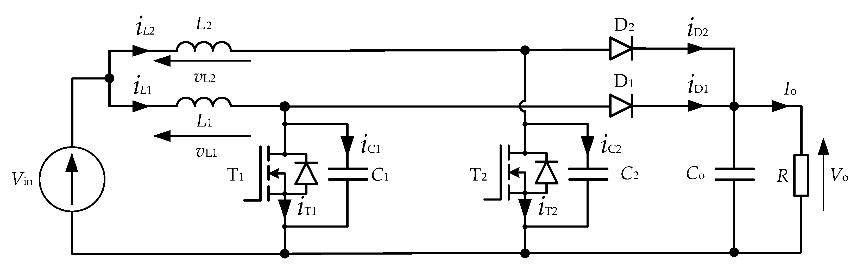
The analyzed converter topology in two-phase variation is presented in
Figure 1. Connecting capacitors
C1 and
C2 in parallel to transistors T
1 and T
2 cause resonance to occur between them and inductors
L1 and
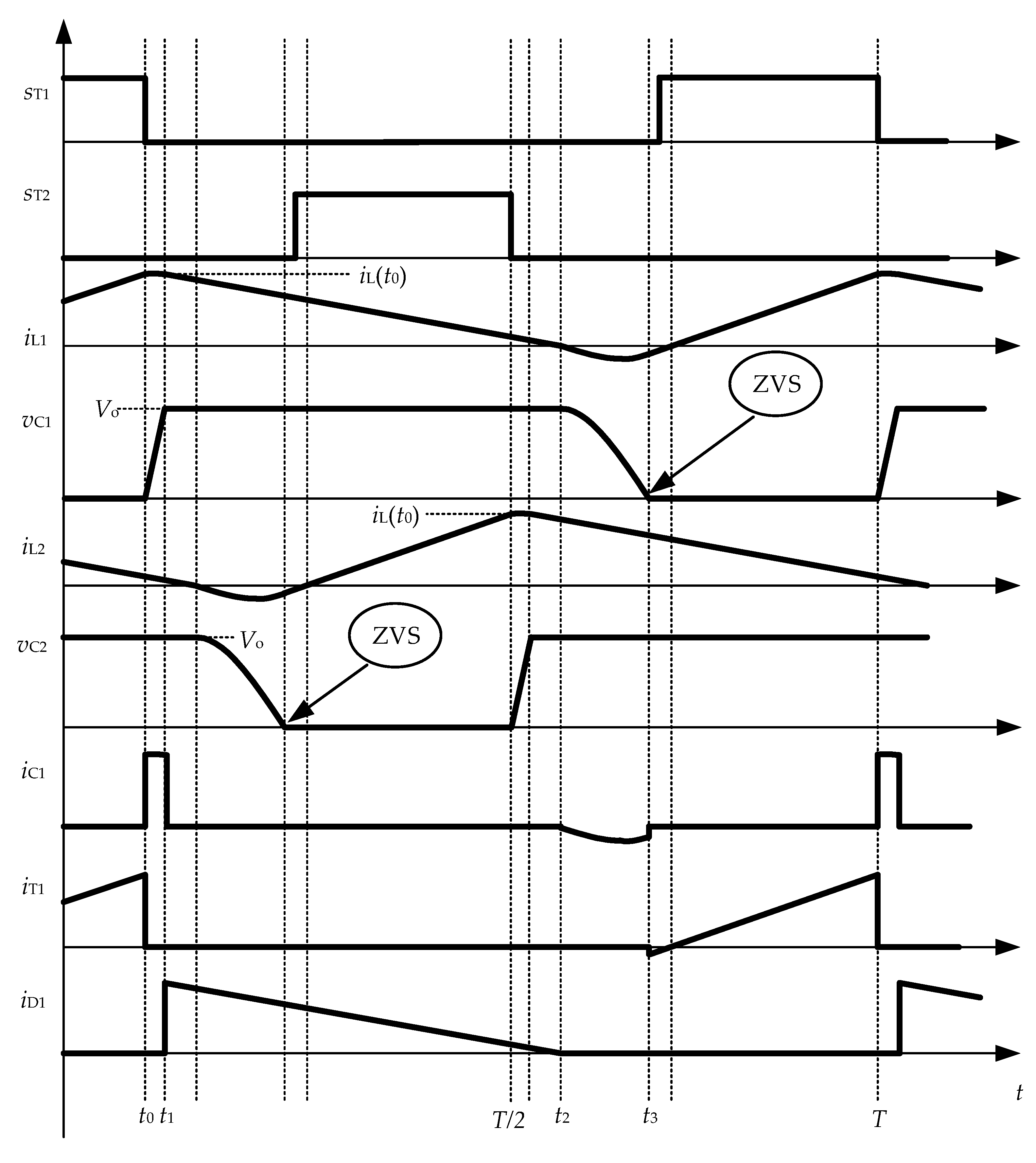
L2, which results in the capacitors being discharged during transistors’ turn off, thus allowing turn-on in zero-voltage conditions. Gate signals of the transistors are phase shifted by 180° to decrease input current ripple, similarly to two-phase interleaved DC/DC converters. Waveforms of the chosen currents and voltages are shown in
Figure 2.
2. Converter Operation Analysis
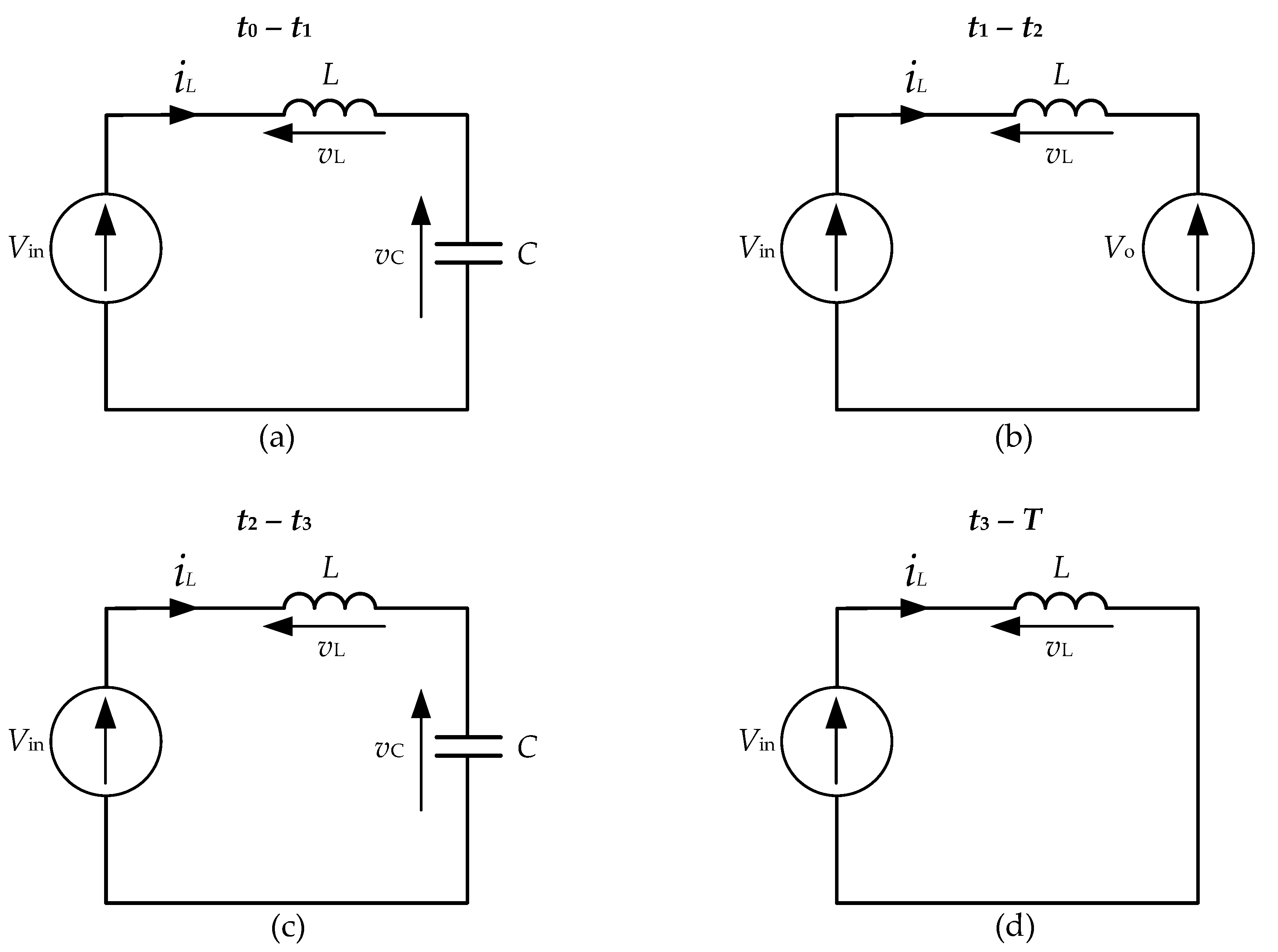
The converter may be analyzed by using four equivalent circuits for one phase of the converter solely. Those equivalent circuits are presented in
Figure 3 and are related to the timestamps highlighted in
Figure 2. It is assumed that:
to simplify the analysis. The following variables are defined:
where
ω0 is the resonant angular frequency,
Z0 is the characteristic impedance of the resonant circuit,
is the normalized load resistance, and
G is the converter voltage ratio.
Differential equations may be composed for each of the four equivalent circuits, allowing for the calculation of the time intervals. These time intervals are equal to:
The converter may be further analyzed by assuming that the input energy is equal to the output energy and by replacing the voltage supply
Vin with a current source
J where
J is equal to the average value of the input current. The average voltage on the current source is equal to the average voltage on the resonant capacitor
C, as the average voltage on the inductor
L is equal to zero. Thus the input energy is equal to:
During the last state of operation (
t3 −
T) the voltage
vC is zero, thus the input energy equation can be written as:
Output energy is equal to:
By assuming equality of input and output energy the following implicit equation can be derived:
where
N is the number of phases of the converter,
f0 is the resonant frequency, and
fs is the switching frequency. A detailed derivation of (13) is presented in
Appendix A.
3. Soft Switching Conditions
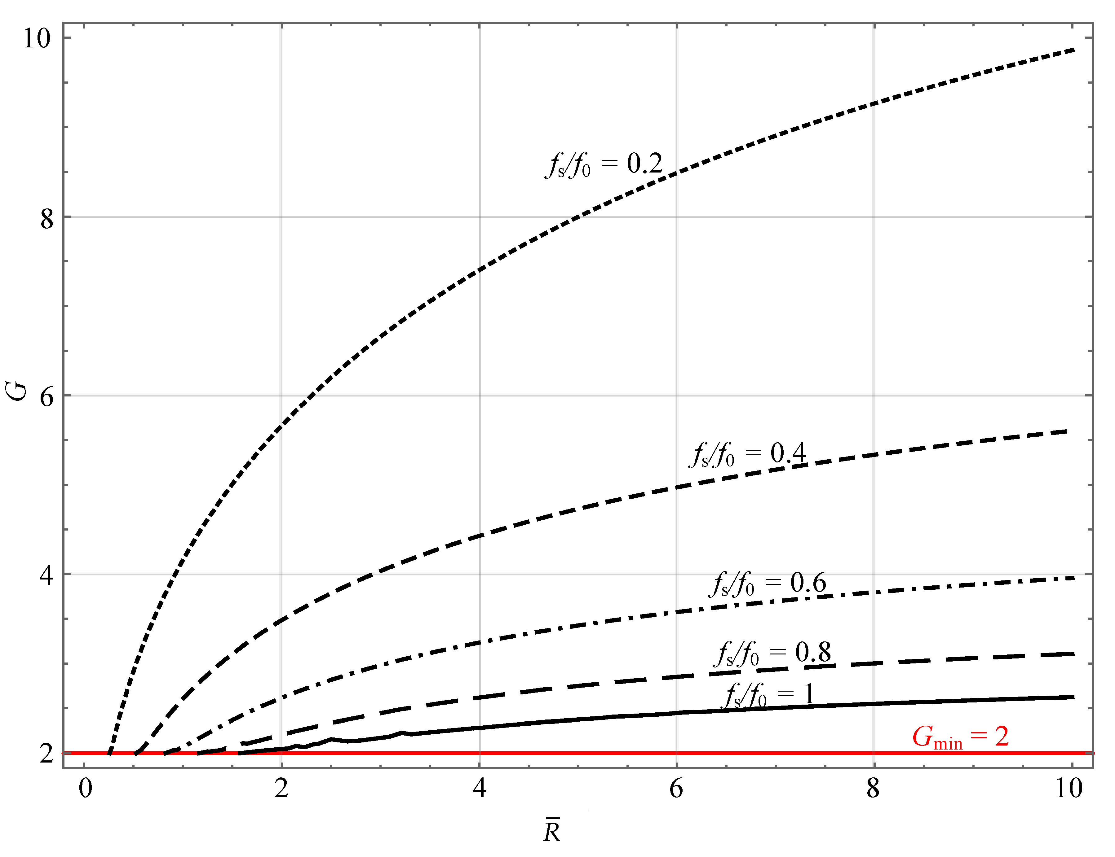
Equation (13) allows for plotting the voltage ratio
G as a function of normalized switching frequency
fs/
f0 for set values of
and
N. An example is shown in
Figure 4, for different values of
and
N = 2 (two-phase converter). Switching frequency of the converter should not exceed the resonant frequency to ensure proper operation of the converter. Conditions for soft switching can also be found by analyzing (13). The value under the square root sign must be equal to or greater than zero. Therefore the following soft switching condition can be found:
which yields:
Conditions for soft switching are highlighted in
Figure 4.
Switching frequency should also be limited to ensure that the switching period is longer than the resonant period, thus implementing another condition:
However, because of the characteristic of voltage ratio
G as a function of normalized resistance
it may be impossible to obtain
G at a desirable value for high values of
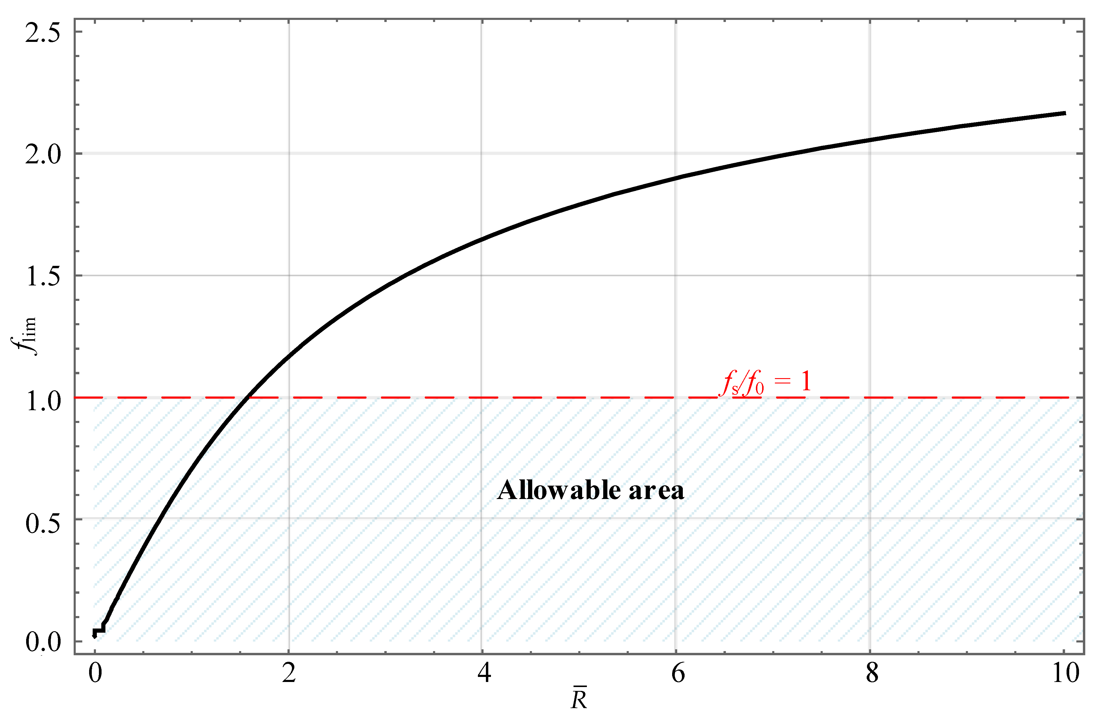
while keeping the switching frequency below resonant frequency. In order to present this property of the converter the limit frequency
flim has been calculated and plotted as a function of normalized resistance
. Limit frequency
flim is defined as a value of
fs/
f0 that results in
G =
Gmin = 2 for a given value of
. The results are plotted in
Figure 5. The plot was obtained by using Equation (13) and assuming that
G = 2.
By analyzing the plot given in
Figure 5 one can deduce that for
higher than 1.5 the value of
flim is greater than 1. Therefore the converter can operate at switching frequencies higher than the resonant frequency and achieve ZVS for high enough values of
. However, as mentioned above, normalized switching frequency
fs/f0 should be kept below the value of 1 (shown in
Figure 4 and
Figure 5 by a dashed line).
4. Load Characteristics
Equation (13) can also be used to plot load characteristics (voltage ratio
G as a function of normalized load resistance
. However, it can only be done for given values of normalized switching frequency
fs/
f0. The plot is presented in
Figure 6.
A general conclusion from the load characteristic that can be drawn is that the voltage ratio G increases when increases. Thus for a given value of input voltage Vin = const., the output voltage Vo rises when the load decreases (load resistance R increases).
The characteristics plotted in
Figure 4,
Figure 5 and
Figure 6 are crucial for the process of converter design. For instance one could deduce that the normalized load resistance
should be relatively high, thus making the possible frequency control range wide. In a typical application of such a converter the load resistance
R results from the load itself and does not allow for changing it freely. Therefore the normalized load resistance
can only be increased by decreasing the characteristic impedance
Z0. However, this can lead to an increase of current values in the converter. For example, in the analyzed converter decreasing characteristic impedance
Z0 leads to the increase of transistor turn-off current, which is also the peak current of the inductors (see Equation (A9) in
Appendix A). This affects power loss in the converter and possibly could lead to magnetic core saturation of inductors
L1 and
L2. Therefore inductance
L and capacitance
C should be chosen not only to obtain a desired value of resonant frequency
f0, but also by taking load resistance
R and current values into consideration.
5. Experimental Converter
To confirm the analysis an experimental two-phase converter was constructed and G was measured as a function of fs/f0 for a set value of R = 50 Ω. The experimental converter was designed using the following procedure:
Input data were decided: supply voltage Vin = 50 V, load resistance R = 50 Ω, output power Po up to 1 kW, output voltage Vo up to 250 V, voltage ratio range G = 2.5–5, switching frequency range fs = 200–500 kHz.
By reading
Figure 4 it was deduced that for the chosen voltage ratio range a normalized load resistance value
in the range of 1.5–2.5 and normalized switching frequency
fs/
f0 in the range of 0.25–0.6 is suitable. For the chosen switching frequency range this results in a required value of the resonant frequency
f0 = ca. 800 kHz.
In order to keep maximum current values in the circuit possibly low it was decided that the normalized load resistance should be kept close to the lower boundary of the chosen range, thus Z0 was chosen to be 30 Ω which would result in = 1.67.
Assuming Z0 = 30 Ω and ω0 = 2π∙800 kHz and using Equations (3) and (4) L and C were calculated, resulting in L = 5.96 µH and C = 6.63 nF.
By analyzing the market of available capacitors final value of capacitance C was chosen to be 6.6 nF. The final value of inductance L was set experimentally by using the available ferrite cores and litz wire to be L = 5.8 µH.
The parameters of the converter designed with the above procedure are provided in
Table 1.
Gallium nitride TPH3207WS transistors and silicon carbide STPSC1006D diodes were used as power semiconductors. By changing the switching frequency the voltage ratio G was measured for constant values of Vin and R. The measurements were conducted in the following conditions:
Frequency range: fs = (200–400) kHz which corresponds to fs/f0 ≅ 0.25–0.5, with a step of 10 kHz,
Supply voltage Vin = 50 V,
Load resistance R = 50 Ω, which results in = 1.68.
Temperature of the transistors was also measured to ensure that each data point was recorded at thermal steady state.
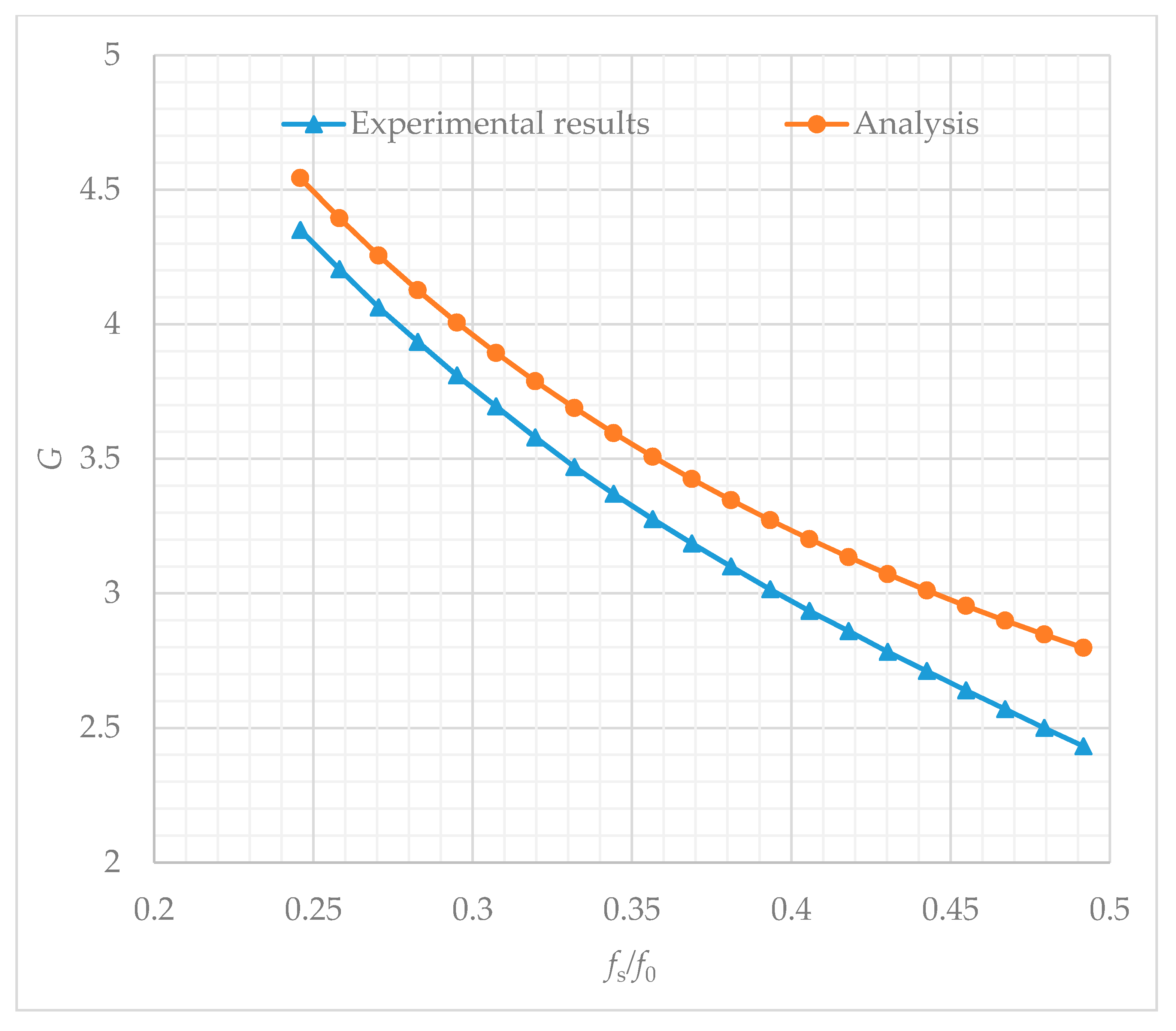
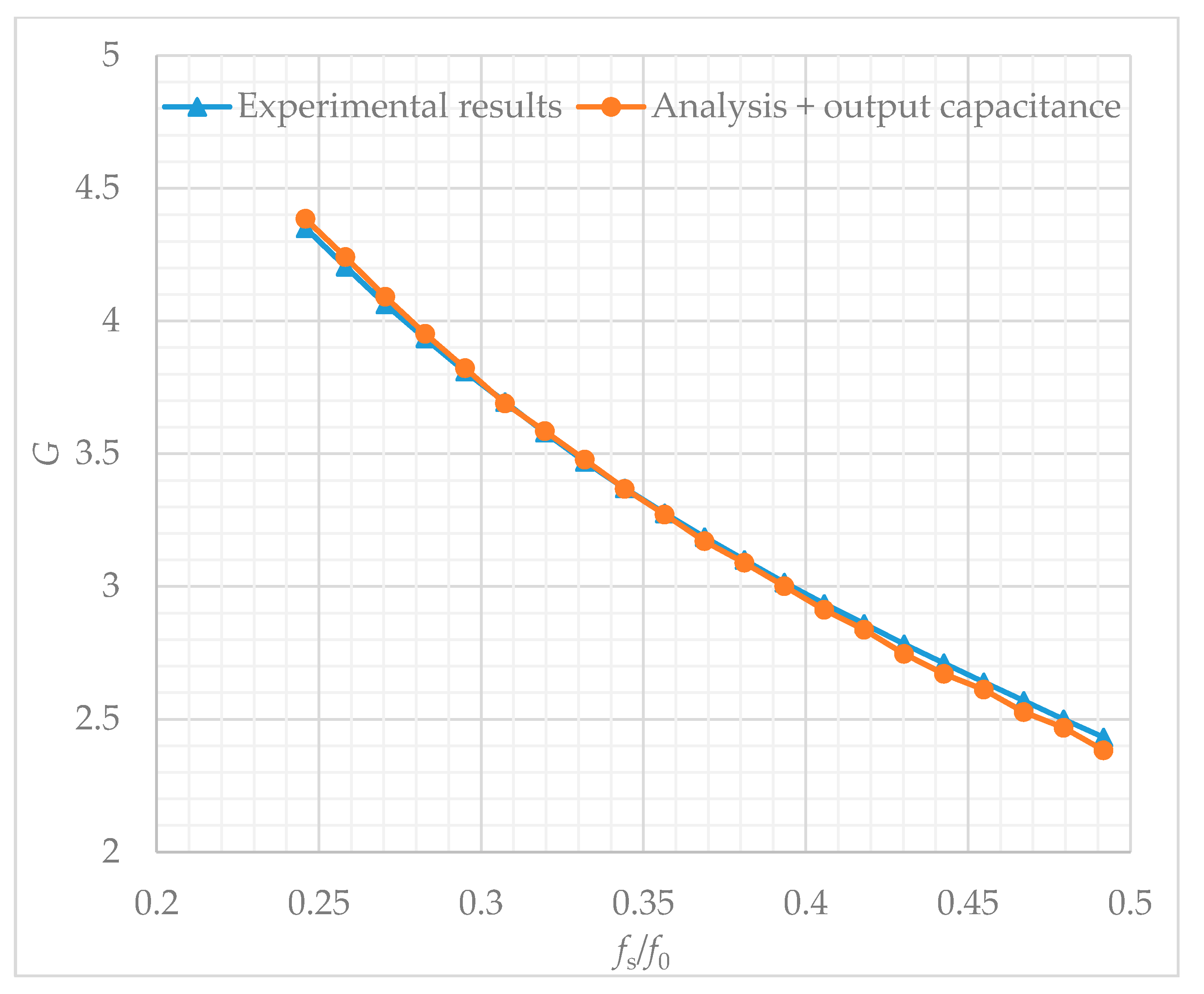
Voltage ratio was also calculated numerically for the same sets of parameters using equation (13). Both data sets were plotted and are presented in
Figure 7. It can be seen that the experimental results differ from the calculated voltage ratio throughout the whole range of data points. The difference is lower for higher values of
G, but it remains at a value of around 0.2, which makes it difficult to predict the output voltage at a given value of
Vin,
, and
fs/
f0.
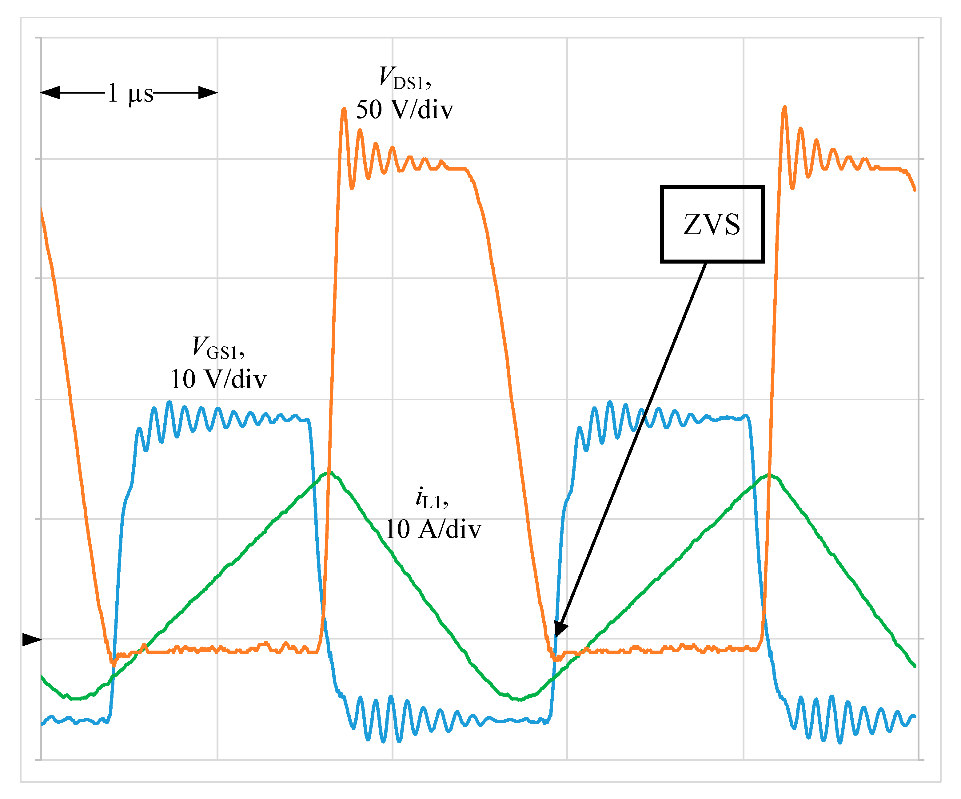
Figure 8 presents waveforms of the gate-source voltage and drain-source voltage of transistor T
1 and the current of inductor
L1, thus showing how one of the phases operates. It can be seen that in steady-state the transistor is turned on in zero-voltage conditions.
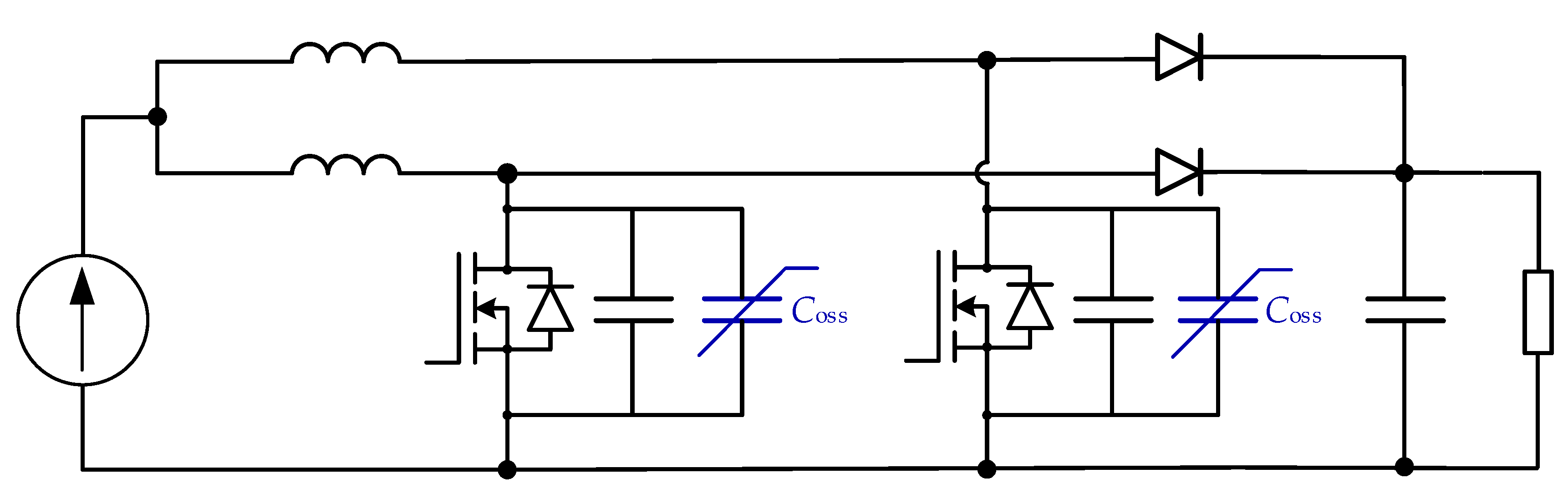
6. Influence of Output Capacitance
A possible explanation for the differences shown in
Figure 7 is the impact of output capacitance
Coss on the resonant frequency, as it is connected in parallel to the resonant capacitors, as shown in
Figure 9. The total resonant capacitance is the sum of the used capacitor
C and the output capacitance
Coss. Therefore Equation (3) must be altered to:
Output capacitance increases the resonant capacitance, therefore decreasing the resonant frequency which for a switching frequency value fs results in a lower normalized frequency fs/f0. However, because of the nonlinear character of Coss its impact on the resonant frequency is variable.
Discharging of resonant capacitance begins when its voltage is equal to
Vo. Therefore
Coss is a function of
Vo, thus making it variable with
Vin and
fs. Output capacitance especially impacts the resonant frequency at low voltages, as
Coss usually gets lower at higher voltages. To consider
Coss in calculations using Equation (13) the plot given in the transistors’ datasheet was digitized and the resonant frequency and characteristic impedance value were updated at each calculated point. The analysis shown in
Figure 7 was redone and plotted, as shown in
Figure 10. The same experimental results were used to compare them with redone calculations. As it can be seen both curves are nearly identical, with the highest difference in
G being below 0.05. Therefore including
Coss in calculations is necessary to obtain results similar to the physical converter. The results can also explain why the difference between the analytical results and experimental measurements is larger at higher values of normalized switching frequency. As the switching frequency rises the output voltage gets lower (
Figure 4), thus resulting in the growth of the output capacitance
Coss. Therefore the difference between the additional capacitance
C and its sum with the output capacitance rises thus increasing the discrepancy between both curves. The analysis of output capacitance influence on the voltage ratio could also lead to an interesting deduction. Namely the analyzed converter topology would achieve different voltage ratios for the same values of normalized switching frequency and normalized load resistance, if the input voltage varied. Because of the variation of input voltage, the output voltage would change, thus changing the output capacitance, which would in turn impact the resonant frequency.
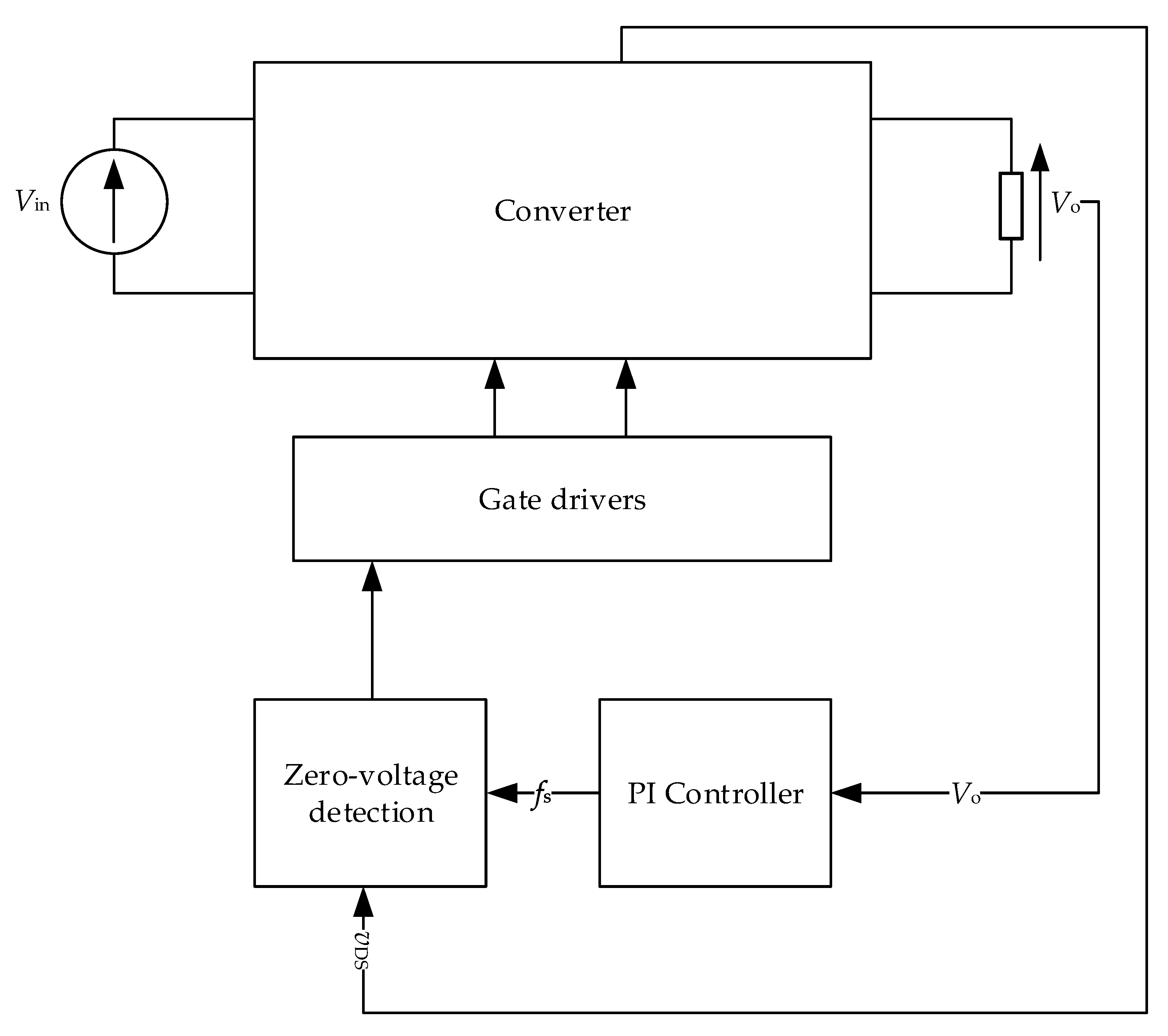
7. Possible Output Voltage Regulation Method
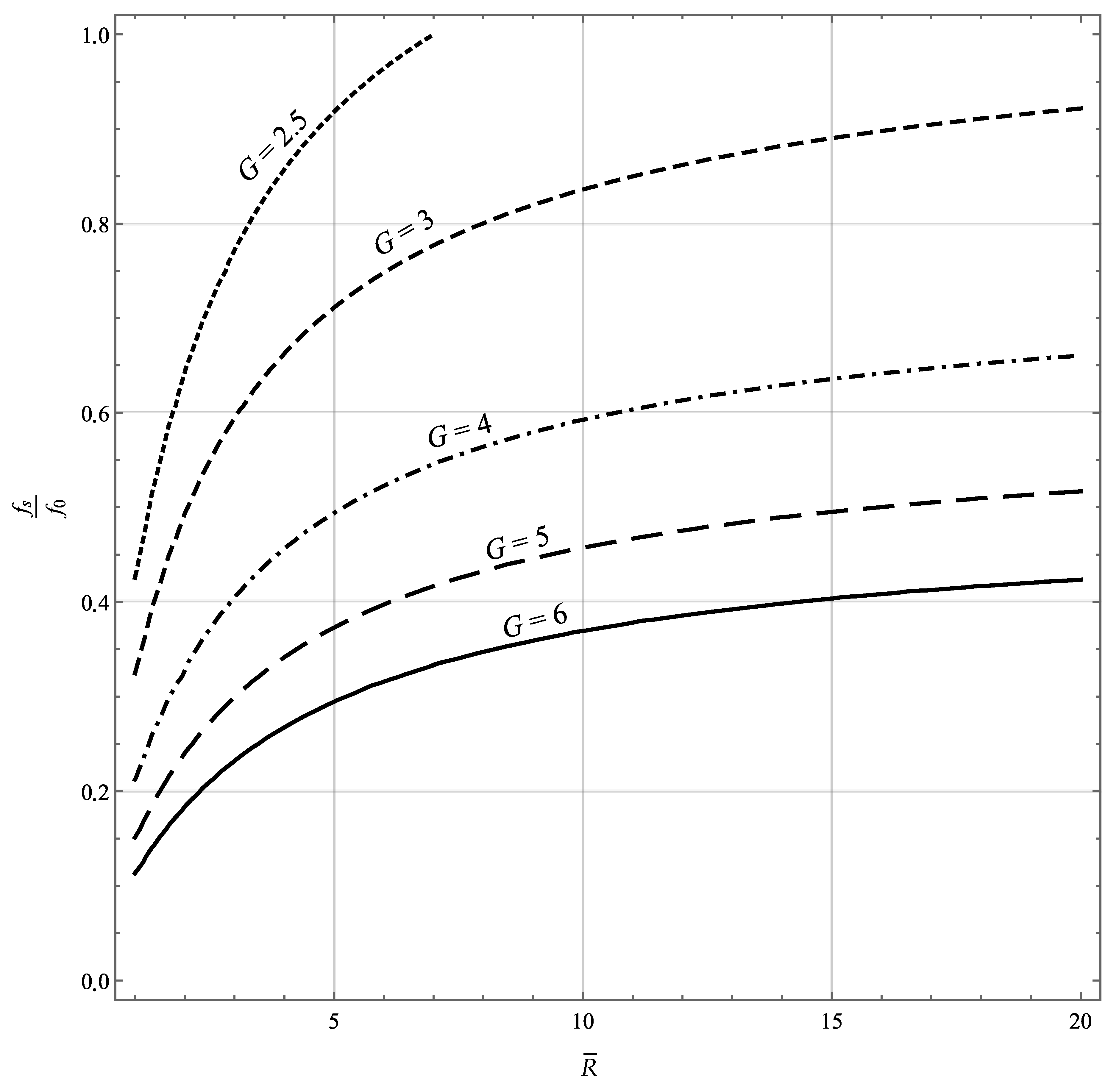
Applying the analyzed converter in any real energy generation system, for example as a boost stage in a photovoltaic inverter, requires a control method that allows to regulate the output voltage to be developed. The voltage ratio plot, presented in
Figure 4, can be used to propose such a controller. Voltage ratio
G and normalized load resistance
are variables that change in a renewable energy generation system, as the input voltage and the load vary. Thus maintaining constant output voltage
Vo requires switching frequency
fs to change as the input voltage
Vin and load resistance
R fluctuate.
Equation (13) allows for plotting normalized switching frequency
fs/
f0 as a function of normalized load resistance
by assuming that supply voltage
Vin = const. and voltage ratio
G = const. Such a plot, for several given values of voltage ratio
G is presented in
Figure 11. The plot reveals the main limitation of the converter, namely that it is not possible to keep the voltage ratio low at low load condition (when the load resistance is high). For example keeping the voltage ratio at
G = 2.5 at normalized load resistance
greater than 7 would require normalized switching frequency
fs/
f0 to be above 1.
However,
Figure 4 and
Figure 11 combined, show that it is indeed possible to control the output voltage by changing the switching frequency. A simplified schematic of the proposed controller is presented in
Figure 12. This method requires the output voltage and drain-source voltages of the transistors to be measured. A PI controller is used to change the switching frequency in order to change the output voltage. A zero-crossing detection block is needed to ensure that the switches are turned on in zero-voltage conditions.
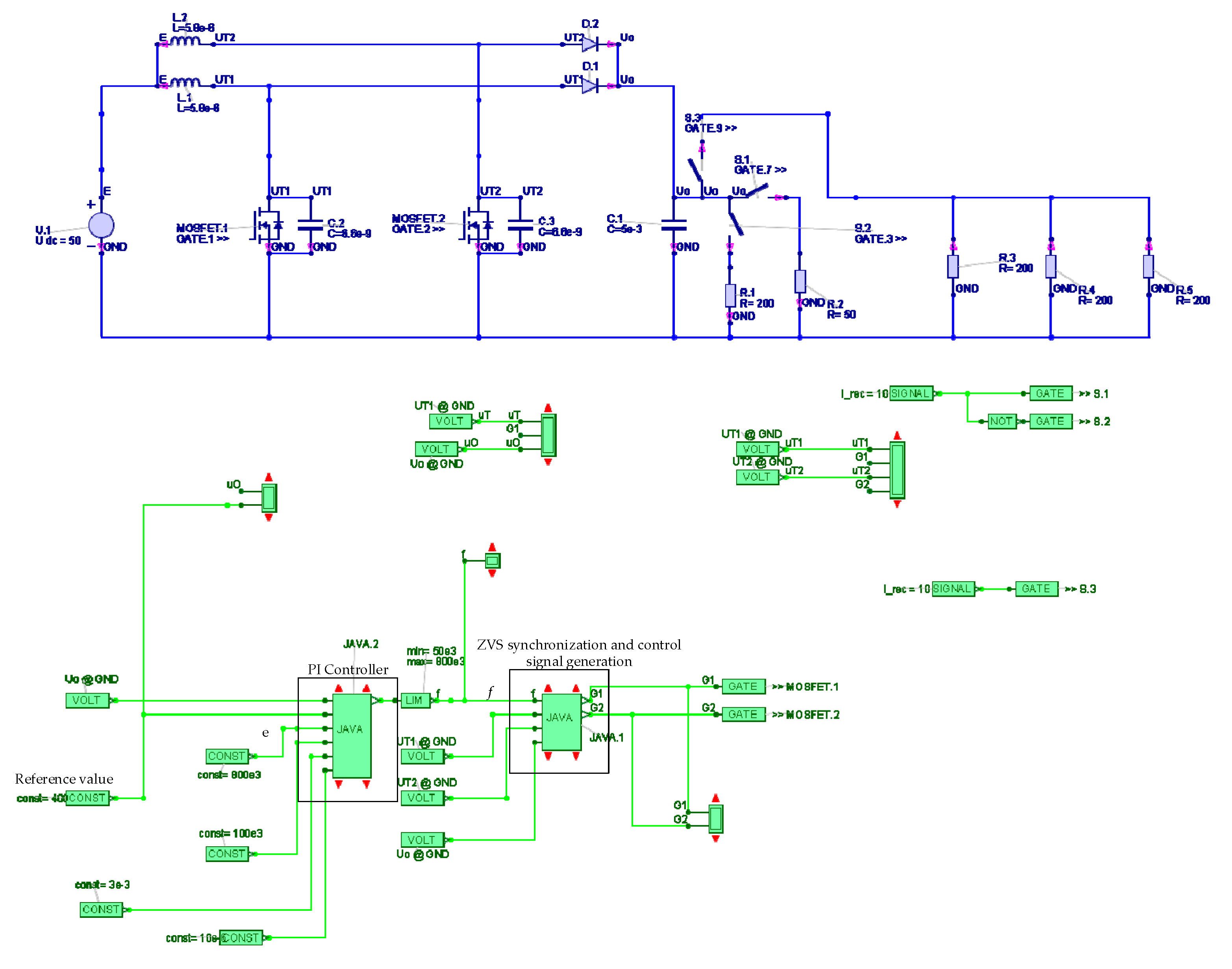
In order to confirm feasibility of the proposed control method a simulation model was built in GeckoCircuits software. An overview of the model is presented in
Figure 13. All circuit parameters are the same as in the experimental converter. The model allows for simulation of certain dynamic states—step of desired output voltage and sudden load resistance variation. Both the PI controller and ZVS synchronization block were programmed in Java programming language. The resonant frequency is around 813 kHz, thus the switching frequency was limited to the range of 50–800 kHz. The PI controller was tuned by trial and error method while analyzing the step response. The output value of the PI controller is the switching frequency which is then the input of the ZVS synchronization block, which has additional inputs—drain-source voltages of the MOSFETs. The MOSFETs are turned on when their drain-source voltage reaches zero, while turn-offs result from the switching period. The same block is also responsible for phase shifting both control signals.
However, when the output voltage is too low, i.e., when the voltage ratio G is below 2, for example during the converter start-up, zero-voltage switching is not achievable as was shown before. Therefore control signals would not be turned high at any point. Thus another condition was implemented—when the output voltage Vo is lower than 210% of the input voltage Vin the MOSFETs are switched with a constant duty cycle D = 0.5 and switching frequency fs = 50 kHz. After Vo reaches 2.1Vin control signals are synchronized to ZVS conditions.
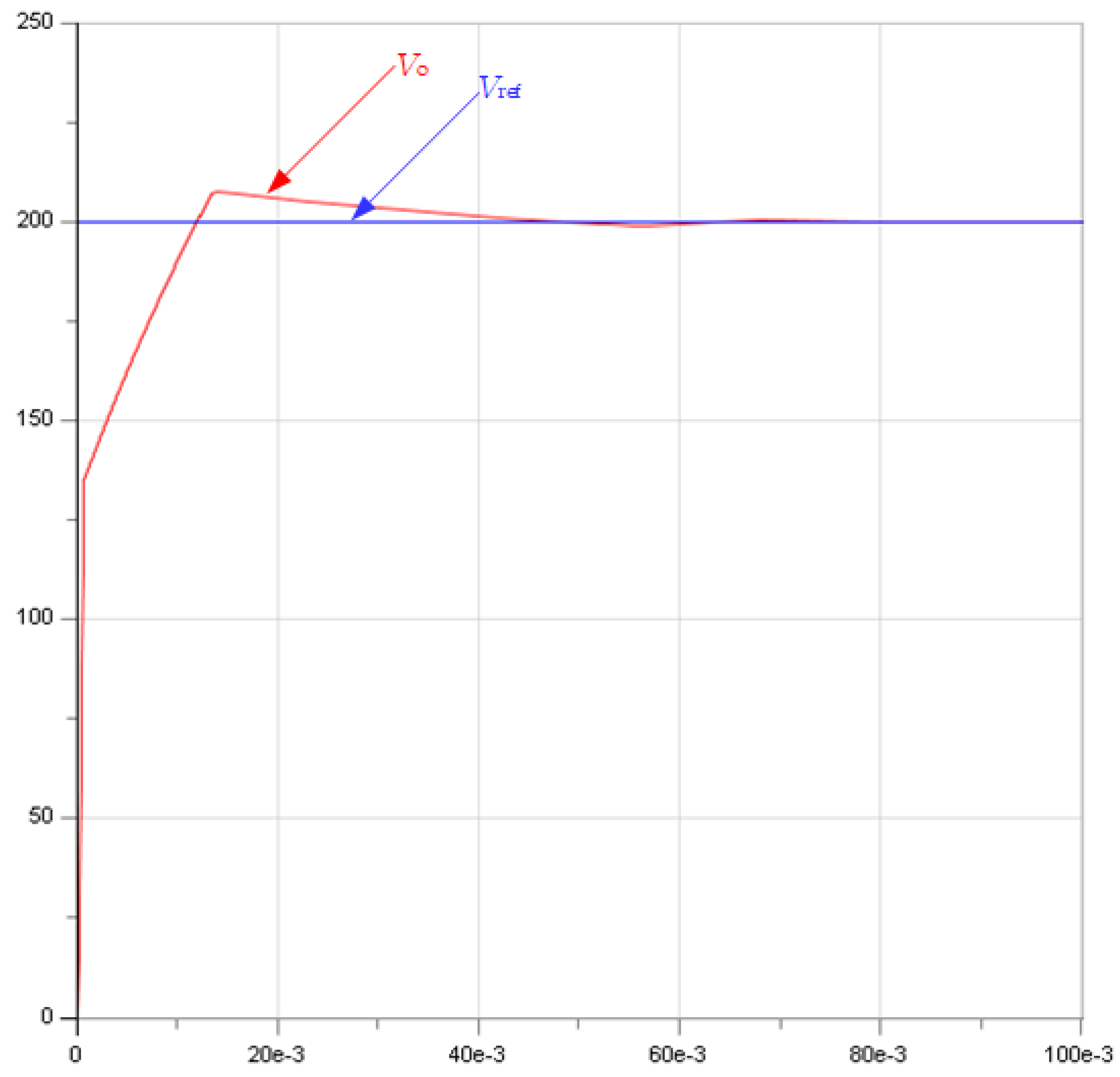
The model was simulated for two main scenarios, possible in a real application:
Scenario 1: start-up of the converter and step response for reference output voltage set to 200 V and 50 Ω load resistance;
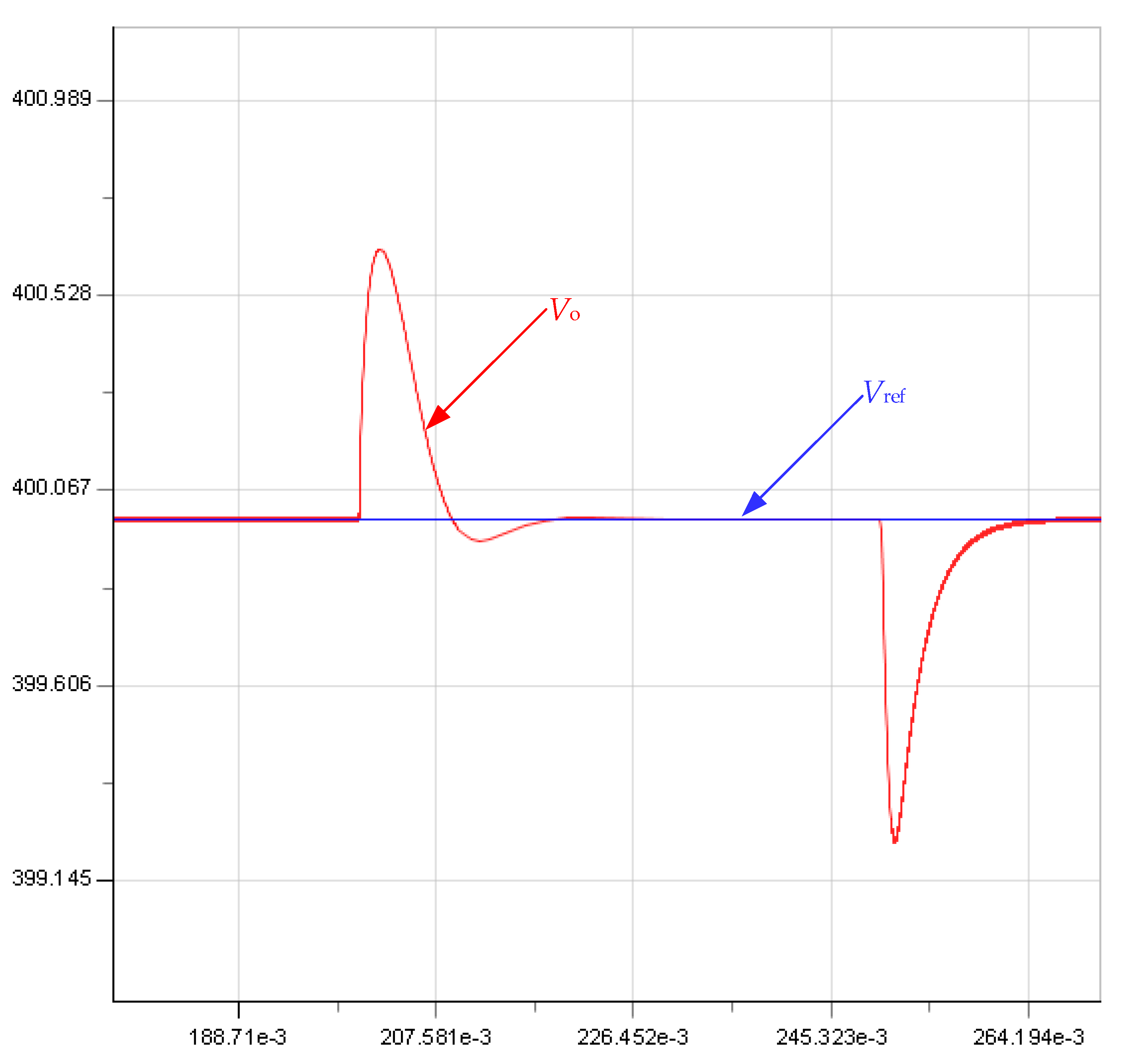
Scenario 2: sudden change of the load resistance from R = 50 Ω to 200 Ω and subsequently back to 50 Ω for Vref = 400 V.
The results of both simulations show that the proposed control method is feasible, thus making the analyzed converter topology applicable in renewable energy generation systems, other DC power supplies or as a boost stage in any device. It is possible to control the output voltage with little overshoot, which could be further reduced by fine-tuning the PI controller. The output voltage can also be controlled for different load resistance values.
However implementing the proposed control method in a prototype converter requires further analysis of extreme work conditions, such as very or very low loads. For example, a very low load (high load resistance) could result in the voltage ratio rising above the voltage rating of the converter components, which would lead to damaging the converter. Therefore over-voltage detection and protection are most likely required. Despite that the controller must be able to control the output voltage even for very low loads, thus a feasible solution to the described problem must be found. A possible solution could be the implementation of a “cutoff” mode, similarly to LLC resonant converters. Further work is needed to confirm the feasibility of such a solution in a prototype setup.
8. Conclusions
In this paper interleaved quasi-resonant zero-voltage switching boost converters are analyzed. A new formula for the voltage ratio is derived for a converter of any number of phases. It ties the output voltage with switching frequency and load resistance. However, its implicit form makes it necessary to use numerical methods to solve the equation for a given set of parameters.
The analysis led to formulating the conditions for soft switching which were then further analyzed and certain characteristics of the converter could be plotted. Namely the relation between voltage ratio G, normalized switching frequency fs/f0, and normalized load resistance were presented as several families of characteristics. The limiting factor of high load resistance was recognized and described as a potential problem for regulation of output voltage.
The impact of normalized load resistance was further investigated and described. It was found that a compromise between normalized load resistance and characteristic impedance Z0 must be found in order to limit the transient currents of the converter while allowing for output voltage regulation.
An experimental two-phase converter was built and tested. The results of the experiments were compared to the values calculated using the derived formula. A difference was recognized and a possible explanation was given. Namely parasitic output capacitance of the transistors Coss was pointed out as the reason for lower voltage ratio, as its influence lowers the resonant frequency.
Output capacitance Coss was taken into account in calculations and compared to the previously achieved experimental results. Much closer results, with calculated and measured voltage ratio remaining within 0.05 of each other in the range of 2.4 to 4.5, were obtained. Therefore it was concluded that the derived formula is useful to predict and control output voltage of the analyzed converter topology, provided that transistors’ output capacitance is considered in calculations.
Real-life applications of such a converter require it to be able to produce a desired value of output voltage for a wide range of input voltage and load resistance values. Thus a control method for the converter was proposed and a simulation model was built to confirm its feasibility. The simulations have shown that it is indeed possible to control the output voltage but certain limitations occur. Namely at low or no load conditions the voltage ratio G rises, making the output voltage high and thus possibly leading to damage of the converter components or the supplied load itself. A possible solution was proposed, namely a “cutoff mode” implementation, similar to LLC resonant converters, where the transistors are switched in short “bursts” to keep the output voltage at a desired value.
Further work should be done, focusing on implementing the proposed control method in a prototype converter while solving the problem of regulating the output voltage at low load conditions. Extreme high load conditions should also be analyzed and both over-current and over-voltage protection should be implemented.
Author Contributions
Conceptualization, P.Z. and M.K.; methodology, P.Z.; software, P.Z.; validation, P.Z., M.K. and K.K.; formal analysis, P.Z., M.K. and K.K.; investigation, P.Z. and K.K.; data curation, P.Z.; writing—original draft preparation, P.Z.; writing—review and editing, P.Z., M.K. and K.K.; supervision, M.K.; funding acquisition, P.Z. All authors have read and agreed to the published version of the manuscript.
Funding
This research was supported by Silesian University of Technology’s internal scholarship fund for the year 2020.
Conflicts of Interest
The authors declare no conflict of interest.
Appendix A
A detailed derivation of Equation (13) is given in the
Appendix A. By assuming the input power is equal to the output power the current source
J current value may be defined as:
After integrating (11) and using (12) and (A1) the following is obtained:
By solving differential equations for the equivalent circuits shown in
Figure 3 the value of
t1 may also be calculated as:
thus:
Similarly
iL(
t3) can be obtained:
Substituting (A4) and (A5) into (A2) yields:
The average current flowing to the output from each phase can be determined by analyzing the waveforms in
Figure 2 and it is equal to:
substituting (8) and (A4) into (A7) and using Ohm’s law yields:
which can be further transformed into:
By substituting (A9) into (A6) and further transforming (A6) the following is obtained:
It can be seen that
is equal to
,
is equal to
and
equals
. By using these equalities and substituting the voltage ratio
G into (A10) the final form of the implicit equation given by (13) is obtained:
References
- BP. Statistical Review of World Energy, 69th ed.; 2020; Available online: https://www.bp.com/content/dam/bp/business-sites/en/global/corporate/pdfs/energy-economics/statistical-review/bp-stats-review-2020-full-report.pdf (accessed on 20 November 2020).
- Zhao, B.; Abramovitz, A.; Liu, C.; Yang, Y.; Huangfu, Y. A Family of Single-Stage, Buck-Boost Inverters for Photovoltaic Applications. Energies 2020, 13, 1675. [Google Scholar] [CrossRef] [Green Version]
- Balaji, C.; Chellammal, N.; Sanjeevikumar, P.; Subramaniam, U.; Holm-Nielsen, J.B.; Leonowicz, Z.; Masebinu, S.O. Non-Isolated High-Gain Triple Port DC-DC Buck-Boost Converter with Positive Output Voltage for Photovoltaic Application. IEEE Access 2020, 8, 113649–113666. [Google Scholar] [CrossRef]
- Chub, A.; Vinnikov, D.; Kosenko, R.; Liivik, E. Wide Input Voltage Range Photovoltaic Microconverter with Reconfigurable Buck–Boost Switching Stage. IEEE Trans. Ind. Electron. 2017, 64, 5974–5983. [Google Scholar] [CrossRef]
- Hamanaka, M.; Matsuyama, T.; Mizuno, K.; Yukita, K.; Matsumura, T.; Goto, Y. Development of a Buck-Boost Convertor for Photovoltaic Systems using GaN Power Devices. In Proceedings of the 2018 IEEE International Telecommunications Energy Conference (INTELEC), Turin, Italy, 7–11 October 2018; pp. 1–5. [Google Scholar] [CrossRef]
- Liu, J.; Zheng, Z.; Wang, K.; Li, Y.D. Comparison of boost and LLC converter and active clamp isolated full-bridge boost converter for photovoltaic DC system. J. Eng. 2019, 2019, 3007–3011. [Google Scholar] [CrossRef]
- Malik, M.Z.; Haoyong, C.; Nazir, M.S.; Khan, I.A.; Abdalla, A.N.; Ali, A.; Chen, W. A New Efficient Step-Up Boost Converter with CLD Cell for Electric Vehicle and New Energy Systems. Energies 2020, 13, 1791. [Google Scholar] [CrossRef] [Green Version]
- Zhang, Y.; Sun, J.-T.; Wang, Y.-F. Hybrid Boost Three-Level DC–DC Converter with High Voltage Gain for Photovoltaic Generation Systems. IEEE Trans. Power Electron. 2012, 28, 3659–3664. [Google Scholar] [CrossRef]
- Hassan, W.; Lu, Y.; Farhangi, M.; Lu, D.D.-C.; Xiao, W. Design, analysis and experimental verification of a high voltage gain and high-efficiency DC–DC converter for photovoltaic applications. IET Renew. Power Gener. 2020, 14, 1699–1709. [Google Scholar] [CrossRef]
- Spiazzi, G.; Buso, S. Analysis of the Interleaved Isolated Boost Converter with Coupled Inductors. IEEE Trans. Ind. Electron. 2014, 62, 4481–4491. [Google Scholar] [CrossRef]
- Lee, H.-S.; Yun, J.-J. Quasi-Resonant Voltage Doubler with Snubber Capacitor for Boost Half-Bridge DC–DC Converter in Photovoltaic Micro-Inverter. IEEE Trans. Power Electron. 2018, 34, 8377–8388. [Google Scholar] [CrossRef]
- Li, Q.; Wolfs, P. An Analysis of the ZVS Two-Inductor Boost Converter under Variable Frequency Operation. IEEE Trans. Power Electron. 2007, 22, 120–131. [Google Scholar] [CrossRef]
- Jung, D.-Y.; Ji, Y.-H.; Park, S.-H.; Jung, Y.-C.; Won, C.-Y. Interleaved Soft-Switching Boost Converter for Photovoltaic Power-Generation System. IEEE Trans. Power Electron. 2010, 26, 1137–1145. [Google Scholar] [CrossRef]
- York, B.; Yu, W.; Lai, J.-S. An Integrated Boost Resonant Converter for Photovoltaic Applications. IEEE Trans. Power Electron. 2012, 28, 1199–1207. [Google Scholar] [CrossRef]
- Bossche, A.V.D.; Valtchev, V.; Ghijselen, J.; Melkebeek, J. Two-phase zero-voltage switching boost converter for medium power applications. In Proceedings of the Conference Record of 1998 IEEE Industry Applications Conference. Thirty-Third IAS Annual Meeting, St. Louis, MO, USA, 12–15 October 1998; pp. 1546–1553. [Google Scholar] [CrossRef]
Figure 1.
Examined converter topology.
Figure 1.
Examined converter topology.
Figure 2.
Waveforms of chosen voltages and currents in the analyzed converter.
Figure 2.
Waveforms of chosen voltages and currents in the analyzed converter.
Figure 3.
Equivalent circuits of one phase of the converter in four states of operation. (a) Initial resonant capacitor charging after transistor turn-off; (b) Current flowing to the output through the diode; (c) Resonant discharging of the capacitor; (d) Charging the inductor after transistor turn-on.
Figure 4.
Plot of the voltage ratio G as a function of normalized switching frequency for N = 2 and different values of .
Figure 4.
Plot of the voltage ratio G as a function of normalized switching frequency for N = 2 and different values of .
Figure 5.
Plot of the limit frequency flim as a function of normalized load resistance for N = 2.
Figure 5.
Plot of the limit frequency flim as a function of normalized load resistance for N = 2.
Figure 6.
Plot of the voltage ratio G as a function of normalized load resistance for N = 2 and different values of normalized switching frequency fs/f0.
Figure 6.
Plot of the voltage ratio G as a function of normalized load resistance for N = 2 and different values of normalized switching frequency fs/f0.
Figure 7.
Plot of the voltage ratio G as a function of normalized switching frequency for N = 2, = 1.68.
Figure 7.
Plot of the voltage ratio G as a function of normalized switching frequency for N = 2, = 1.68.
Figure 8.
Waveforms of the gate-source voltage, drain-source voltage and phase current of phase 1 with a single turn-on in zero-voltage conditions highlighted 6. Influence of output capacitance
Figure 8.
Waveforms of the gate-source voltage, drain-source voltage and phase current of phase 1 with a single turn-on in zero-voltage conditions highlighted 6. Influence of output capacitance
Figure 9.
Topology of the examined converter with nonlinear parasitic capacitance Coss.
Figure 9.
Topology of the examined converter with nonlinear parasitic capacitance Coss.
Figure 10.
Plot of the voltage ratio G as a function of normalized switching frequency with parasitic capacitance considered for Vin = 50 V, N = 2, R = 50 Ω.
Figure 10.
Plot of the voltage ratio G as a function of normalized switching frequency with parasitic capacitance considered for Vin = 50 V, N = 2, R = 50 Ω.
Figure 11.
Plot of the normalized switching frequency fs/f0 as a function of normalized load resistance for given values of voltage ratio G.
Figure 11.
Plot of the normalized switching frequency fs/f0 as a function of normalized load resistance for given values of voltage ratio G.
Figure 12.
Simplified diagram of the proposed converter control method.
Figure 12.
Simplified diagram of the proposed converter control method.
Figure 13.
Overview of the GeckoCircuits converter model.
Figure 13.
Overview of the GeckoCircuits converter model.
Figure 14.
Start-up and step response of the converter with the proposed control method for Vref = 200 V.
Figure 14.
Start-up and step response of the converter with the proposed control method for Vref = 200 V.
Figure 15.
Response of the converter with the proposed control method during sudden changes in load resistance (from 50 Ω to 200 Ω and back to 50 Ω) for Vref = 400 V.
Figure 15.
Response of the converter with the proposed control method during sudden changes in load resistance (from 50 Ω to 200 Ω and back to 50 Ω) for Vref = 400 V.
Table 1.
Parameters of the experimental converter.
Table 1.
Parameters of the experimental converter.
| Parameter | Value |
|---|
| L | 5.8 μH |
| C | 6.6 nF |
| Z0 | 29.6 Ω |
| R | 50 Ω |
| 1.68 |
| f0 | 813 kHz |
| Publisher’s Note: MDPI stays neutral with regard to jurisdictional claims in published maps and institutional affiliations. |
© 2020 by the authors. Licensee MDPI, Basel, Switzerland. This article is an open access article distributed under the terms and conditions of the Creative Commons Attribution (CC BY) license (http://creativecommons.org/licenses/by/4.0/).


