Article

Thickness Optimization and Photovoltaic Properties of Bulk Heterojunction Solar Cells Based on PFB–PCBM Layer

1
Department of Physics, Faculty of Physical and Numerical Sciences, Abdul Wali Khan University Mardan, Mardan 23200, Pakistan
2
Department of Electronics, Jinnah College for Women, University of Peshawar, Peshawar 25120, Pakistan
3
Institute of Industry Revolution 4.0, Universiti Kebangsaan Malaysia (UKM), Bangi 43600, Malaysia
4
Pak-Austria Fachhochschule Institute of Applied Sciences and Technology, Haripur 22620, Pakistan
5
Department of Electric, Electronics and System Engineering, Faculty of Engineering and Built Environment, Universiti Kebangsaan Malaysia, Bangi 43600, Malaysia
*
Author to whom correspondence should be addressed.
Energies 2020, 13(22), 5915; https://doi.org/10.3390/en13225915
Submission received: 20 September 2020 / Revised: 15 October 2020 / Accepted: 17 October 2020 / Published: 13 November 2020

Abstract

:
We report on the fabrication and study of bulk heterojunction (BHJ) solar cells based on a novel combination of a donor–acceptor poly(9,9-dioctylfluorenyl-2,7-diyl)-co-(N,N0-diphenyl)-N,N′di(p-butyl-oxy-pheyl)-1,4-diamino-benzene) (PFB) and [6, 6]-phenyl-C61-butyric acid methyl ester (PCBM) blend composed of 1:1 by volume. indium tin oxide (ITO)/poly(3,4-ethylenedioxythiophene):poly(styrene sulfonate (PEDOT:PSS)/PFB–PCBM/Ag BHJ solar cells are fabricated by a facile cost-effective spin-coating technique. The thickness of the active film (PFB–PCBM) plays an important role in the efficiency of light absorption, exciton creation, and dissociation into free charges that results in higher power conversion efficiency (PCE). In order to optimize the PCE as a function of active layer thickness, a number of solar cells are fabricated with different thicknesses of PFB–PCBM films at 120, 140, 160, 180, and 200 nm, and their photovoltaic characteristics are investigated. It is observed that the device with a 180 nm thick film demonstrates a maximum PCE of 2.9% with a fill factor (FF) of 53% under standard testing conditions (STC) (25 °C, 1.5 AM global, and 100 mW/cm2). The current–voltage (I-V) properties of the ITO/PEDOT:PSS/PFB–PCBM/Ag BHJ devices are also measured in dark conditions to measure and understand different parameters of the heterojunction. Atomic force microscopy (AFM) and ultraviolet-visible (UV-vis) absorption spectroscopy for the PFB–PCBM film of optimal thickness (180 nm) are carried out to understand the effect of surface morphology on the PCE and bandgap of the blend, respectively. The AFM micrographs show a slightly non-uniform and rough surface with an average surface roughness (Ra) of 29.2 nm. The UV-vis measurements of the PFB–PCBM blend exhibit a reduced optical bandgap of ≈2.34 eV as compared to that of pristine PFB (2.88 eV), which results in an improved absorption of light and excitons generation. The obtained results for the ITO/PEDOT:PSS/PFB–PCBM (180 nm)/Ag BHJ device are compared with the ones previously reported for the P3HT–PCBM blend with the same film thickness. It is observed that the PFB–PCBM-based BHJ device has shown two times higher open circuit voltage (Voc) and, hence, enhanced the efficiency.

1. Introduction

Organic solar cells deliver emission-free low-cost power by converting visible light energy from the sun into electricity. The key benefits of organic solar cells over conventional inorganic cells are their lower cost, easier fabrication, and well-suited with flexible substrates [1,2]. The power conversion efficiency (PCE) of organic solar cells has progressively improved through the use of conjugated polymers [3,4,5]. The complementary properties of high-performance materials are often intentionally combined to acquire the synergy that their combination can deliver [6]. Recently, polymers and their blends, as active layers in the solar cells, have acquired great attention because they can be deposited by simple and inexpensive solution processable techniques [7]. In all polymer solar cells, typically, mixtures of donor and acceptor materials blended in organic solvents are employed to fabricate solar cells, which have the ability to produce an interpenetrating network of heterojunctions throughout the bulk of the active film [8,9]. These solar cells have some ubiquitous benefits: (1) higher absorption of visible light, (2) tunable energy levels, and (3) polymer–polymer blends offer controllable solution viscosity that is a key factor for the production of large-scale organic photovoltaic (OPV) modules [10]. To date, organic solar cells incorporating conjugated polymer/fullerene bulk heterojunction (BHJ) blends have proven to be highly efficient systems [11,12,13]. Semiconducting polymers and fullerene blends ensure efficient charge transfer at the interface [14]. Upon excitation by a photon, excitons (bound electron–hole pairs) are created in semiconducting conjugated polymers. These excitons, when they reach the donor–acceptor interface, are separated with high efficiency, leading to the creation of electrons and holes as individual charge carriers [15]. Many polymers have been used as donors in conjunction with fullerenes which include poly(3-hexylthiophene) (P3HT), poly[N-9′-heptadecanyl-2,7-carbazole-alt- 5,5-(4′,7′-di-2-thienyl-2′,1′,3′-benzothiadiazole) (PCDTBT), poly[[4,8-bis[(2-ethylhexyl)oxy]-benzo[1,2 -b:4,5-b’]-di-thiophene-2,6-diyl][3-fluoro-2-[(2-ethyl-hexyl)-carbonyl]-thieno-[3,4-b]-thiophenediyl]] (PTB7), etc., [13,16,17].
Polymers with fullerene as blends have been extensively probed for the photovoltaic investigations in which P3HT is employed as an electron donor and [6,6]-phenyl-C61 butyric acid methyl ester (PCBM) is employed as an electron acceptor [18,19,20]. In recent years, other alternate electron donor polymers such as PTB7 and (poly[2,1,3-benzothiadiazole-4,7-diyl[4,4-bis(2- ethylhexyl)-4H-cyclopenta[2,1-b:3,4-b’]dithiophene-2,6-diyl]]) (PCPDTBT) have been exploited to demonstrate enhancement in PCEs [21,22]. Polyfluorene-based polymers are an important class of conjugated semiconductors [23] that have potential for high-performance photovoltaic applications [24,25]. Among polyfuorenes, poly-(9,9-dioctylfluorenyl-2,7-diyl)-co-(N,N0-diphenyl)-N,N′di- (p-butyl-oxy-pheyl)-1,4-diamino-benzene) (PFB) possesses extraordinary optical and electrical characteristics such as good electrical conductivity and broad absorption of the solar spectrum [26]. PFB has relatively higher charge carrier mobility and is generally nontoxic. Moreover, PFBs and related copolymers have been investigated for photovoltaic applications by many researchers [27,28]. Recently H. J. Sanith and his co-workers used the PFB:PF8BT blend and achieved a maximum PCE of 2% [10,29]. On the other hand, PCBM and its derivatives are extensively used in the field of organic solar cells due to their promising electronic and optoelectronic properties. PCBM is commonly used as an acceptor material that has high electron affinity and has good conductivity as compared to other molecules. At the same time, PCBM offers its solubility in different organic solvents such as chloroform, dichloroethane, toluene, etc. The energy levels of the highest occupied molecular orbital (HOMO) and lowest unoccupied molecular orbital (LUMO) for PCBM are −6.1 eV and −3.8 eV, respectively, and for PFB, they are −4.3 eV and −2.1 eV, respectively [30,31,32].
As much as the selection of appropriate photoactive materials—donors and acceptors—is important for an efficient solar cell, in similar fashion, a proper thickness of the photoactive film is of the most significance, too [33,34]. Therefore, the thickness of the photoactive film is one of the most important parameters for the high PCE of the solar cell. For instance, if the film is very thin, then the incident light is not fully absorbed by the active film; rather, a small fraction of it is absorbed. So, due to the lower thickness, most of the light is transmitted through the thin film unabsorbed that results in a smaller number of excitons creation and, hence, a few holes and electrons attributes that lead to a low PCE [15]. On the other hand, higher film thickness makes the active layer a better light absorber, which in turn increases the creation of excitons. However, due to the higher thickness of the active film, the exciton’s mean free-path and lifetime are reduced, which are responsible for the recombination of the majority of electrons–holes (vanishing of excitons) without producing free electrons and holes. Whereas, only a few excitons are able to reach the junction and break their bonds between electrons and holes, which produce free electrons and holes [35]. For an optimized PCE of a solar cell, there should be a balance between the absorption of light and the diffusion/dissociation of excitons into free charge carriers, and this can be achieved by preparing an appropriate thickness of the photoactive film [36].
The present work is devoted to introducing a new electron donor polymer—PFB—in BHJ solar cell and investigating the influence of PFB–PCBM active layer thickness on the PCE of ITO/PEDOT:PSS/PFB–PCBM/Ag BHJ solar cells. Moreover, while investigating the BHJ solar cells, we discovered that the performance of PFB–PCBM-based solar cells is greatly controlled by the thickness of the active layer. It is observed that the device with 180 nm PFB–PCBM thin film shows an enhanced efficiency.

2. Materials and Methods

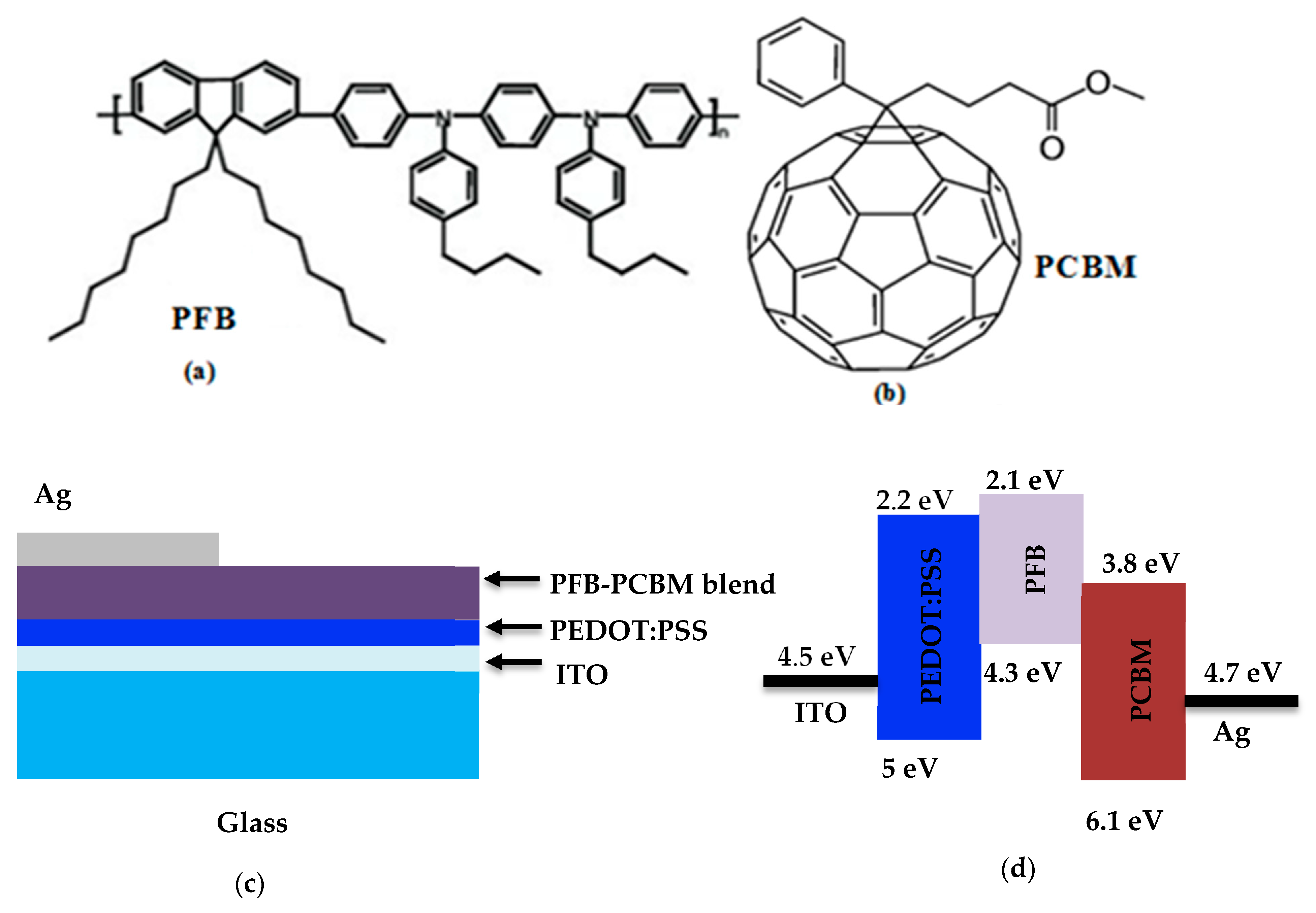
2.1. Material and Device Preparation

The PCBM and PFB were obtained from Sigma Aldrich and Cambridge Display Technology, respectively. Both polymers were used as received. The PFB is used as a donor, whereas PCBM is used as an acceptor. The molecular structure of PFB and PCBM is shown in Figure 1a,b, respectively. For the device fabrication, indium tin oxide (ITO)/glass is used as substrate, which is cleansed in acetone and ethanol by using an ultrasonic tub and dried with nitrogen gas for 5–10 min. A 20 nm layer of poly(3,4-ethylenedioxythiophene):poly(styrene sulfonate (PEDOT:PSS) (Aldrich) is spin coated on the cleaned ITO at 2000 rpm for 20 s using a Laurell WS-400BZ-6NPP/LITE. Then, the sample is annealed using a hot plate for 1 h at 50 °C. The solutions of PFB and PCBM are separately prepared in chloroform at a concentration of 12.5 mg/mL and 25 mg/mL, respectively. The PFB and PCBM blend is prepared by mixing the donor and acceptor solutions in 1:1 by volume. The spin coating technique is employed to deposit an active layer of the PFB–PCBM blend on a pre-cleaned ITO coated glass substrate at the rate of 4000 rpm for 20 s. Then, the sample is dried using a hot plate for 1 h. To complete the device structure, the top metallic silver (Ag) electrode is deposited by the thermal evaporation process using an Edwards auto 306 system. During deposition, the chamber pressure is maintained at 1.5 × 10⁻⁵ mbar with a deposition rate of around of 0.1 nm/s. The electrode thickness obtained is about 80–100 nm. To optimize the PCE of the BHJ solar cell as a function of PFB–PCBM film thickness, several such devices are prepared with different thicknesses of 120, 140, 160, 180, and 200 nm by controlling the spin time and rate of the spin coater during the deposition of films. The structure of the fabricated ITO/PEDOT:PSS/PFB–PCBM/Ag BHJ solar cell and its corresponding energy level diagram under no applied bias are shown in Figure 1c,d, respectively.

2.2. Characterization
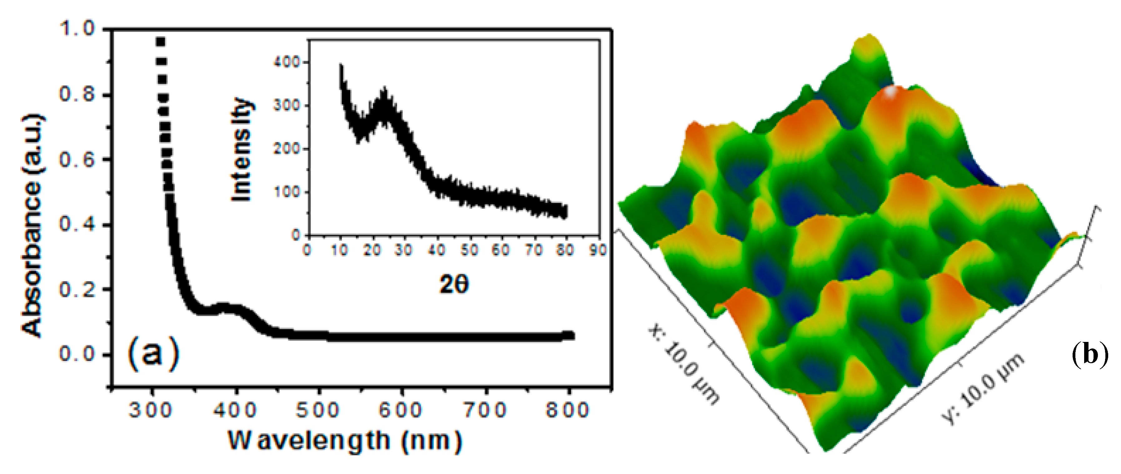
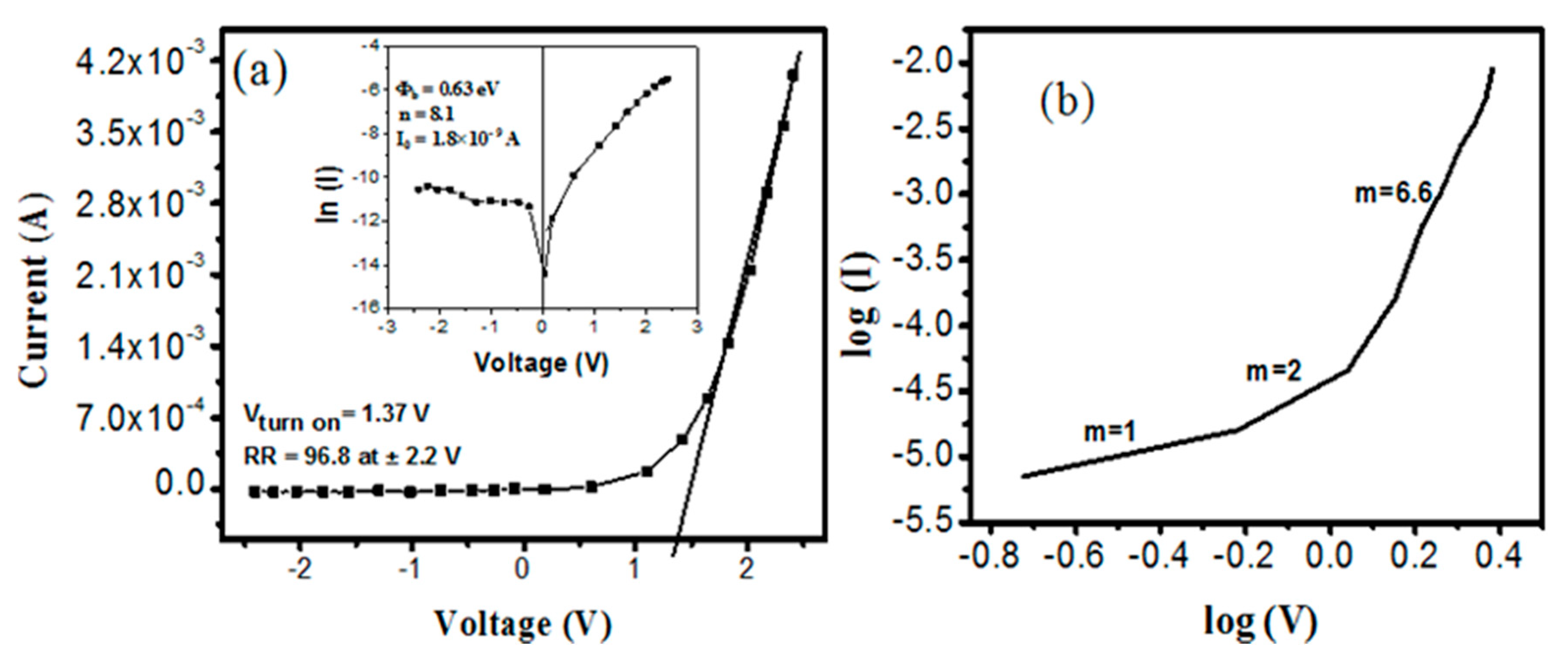
For the characterization of PFB–PCBM, its thin films are deposited on glass substrate by spin coating. Atomic force microscopy (AFM) investigations are carried out in a tapping mode. The AFM scanning frequency is about 0.80 Hz. A Nanosurf 3000 controller model FlexAFM (Probe:NCLR-50) is used to take AFM micrographs. A PerkinElmer Lambda 1050 UV/vis/NIR spectrometry is carried out to measure UV-vis spectrum to obtain an optical bandgap of PFB–PCBM films. The X-ray diffractogram was recorded using PANalytical X’Pert3. Current–voltage (I-V) measurements are done by a Keithley 4200 SMU, while photovoltaic measurements are made under illumination by using a Newport Oriel solar simulator with 1.5 AM filters. The thicknesses of PFB–PCBM films are estimated by a SE850 SENTECH Instruments GmbH profilometer.

3. Results

Figure 2 presents I-V characteristics of ITO/PEDOT:PSS/PFB–PCBM/Ag BHJ solar cells under illumination for various PFB–PCBM film thicknesses i.e., 120, 140, 160, 180, and 200 nm. Sievers et al. have demonstrated that the electrical properties of a device are greatly affected by the thickness of the active layer [37]. In agreement with [37], it can be seen from Figure 2 that the performance of the BJH device in our case also depends upon active layer thickness. The open circuit voltage is almost constant around of 0.90 ± 0.03 V with varying thickness. Nevertheless, the short-circuit current (JSC) and PCE of the BHJ devices change appreciably with thickness. JSC varies from as low as 5 mA/cm2 for the device with an active layer thickness of 120 nm to a maximum of 5.9 mA/cm2 for an active layer thickness of 180 nm. Furthermore, JSC reduces to 5.6 mA/cm2 for the thickness of 200 nm. The fluctuating behavior of JSC for various film thicknesses is analogous to the effect reported elsewhere for poly{[2-methoxy-5-(2-ethylhexyloxy)-1,4-phenylene]vinylene} (MEH–PPV):PCBM based photovoltaic devices. This swaying nature of the device’s performance is ascribed to the carrier generation rate in PFB–PCBM active layers at cathode/polymer interfaces [37]. The device with a film thickness of 180 nm reveals the best PCE as large as 2.9%. Other parameters of the same device are measured as JSC = 5.9 mA/cm2, VOC = 0.93 V, and FF = 53. However, the thickness-dependent PCE decreases beyond the film thickness of 180 nm, which complies with the findings reported by Sievers et al. in [37].
The PCE and fill factor (FF) of ITO/PEDOT:PSS/PFB–PCBM/Ag BHJ solar cell are exclusively plotted as a function of PFB–PCBM film thickness in the inset of Figure 2. The figure shows that the performance of the BHJ device is enhanced as the PFB–PCBM film thickness increases to a certain level. Table 1 summarizes the photovoltaic (PV) parameters (PCE, VOC, ISC, and FF) of the devices at different thicknesses. The results demonstrate that the thickness of the PFB–PCBM blend film has a direct relation with the PCE and FF of the device, which are increasing gradually until 180 nm; however, they decrease beyond 180 nm at 200 nm. Therefore, the optimum film thickness for the PFB–PCBM BHJ cell is 180 nm.
The optimal thin film (180 nm) for a BHJ solar cell is further probed for structural and morphological studies as shown in Figure 3. Figure 3a shows the optical absorption spectra of a PFB–PCBM blend thin film. The spectra exhibit a peak at 390 nm in the visible band. The energy bandgap of the blend was calculated using Tauc’s law, which is given by the following equation:
α E = ( E E g ) m
where α is the coefficient of absorption, E is the energy of the incident photon, Eg represents the bandgap energy, and m is a transition constant/power factor. The relation between absorbance (A), the thickness of the PFB–PCBM film (d), and α is given by:
A = ln [ I I 0 ] A = α d
For the calculation of optical bandgap, the direct permitted transition model is used for PFB–PCBM film. The energy bandgap for PFB is about 2.88 eV [17]. The energy bandgap for the blend was calculated as 2.34 eV, which is close to the value reported elsewhere [18]. The structural analysis of the PFB–PCBM thin film is examined by the XRD technique, which is shown in the inset of Figure 3a. The diffractogram shows no significant peak in the curve, which confirms that the material is amorphous in nature. Figure 3b show a three-dimensional AFM image of PFB–PCBM thin film (180 nm) with a scan size of 10 × 10 µm2. The average/mean surface roughness (Ra) of PFB–PCBM films at 120, 140, 160, 180, and 200 nm is 20.3, 23.9, 26.4, 29.2, and 31.8 nm, respectively, which demonstrate that the films are grown non-uniformly. The estimated average grain size is about 2.1 µm. A detailed morphology of the PFB–PCBM film for the optimum thickness (180 nm) is discussed and shown in Figure 3b which exhibits a coarse texture with broad hill-like peaks and islands. The greater thickness results in an increased surface area of the islands and mosaics. The morphological study carried out by Li and coworkers reveals a correlation between the surface roughness of thin films and the performance of the device, which suggests that the higher surface roughness produces appreciably efficient devices [33]. Rough and non-uniform films are favorable for harvesting more light due to the improved photoabsorption and minimal reflection from the film surface [38]. A probable reason behind the enhanced efficiency of the PFB–PCBM (≈180 nm) solar cell might be the coarse and rough surface of the film that increases the area of contact between the PFB–PCBM film and the metallic contact, leading to efficient charge injection at the interface. The increased surface roughness with broad hill-like peaks tends to collect more light and renders an improved internal reflection, which consequently results in an enhanced device performance. Furthermore, higher roughness also leads to additional defects that can improve exciton disintegration and, hence, charge generation. Since the diffusion length of the charge carriers in polymers is too small and only the carriers generated near the interface contribute toward the photocurrent, hence, the increased contact area would also increase the excess charge generation and gathering at the ITO–polymer interface. The morphology and device performance indicate a successful physical interaction between PFB and PCBM [39]. The improved device performance of the ITO/PEDOT:PSS/PFB–PCBM/Ag BHJ device (≈180 nm) can be attributed to the higher surface roughness and lower optical energy bandgap of the PFB–PCBM blend active layer. A probable reason for the decrease in efficiency at 200 nm is the reduction in the amount of the carriers that reach the charge extraction layer.
The I-V properties of an ITO/PEDOT:PSS/PFB–PCBM/Ag BHJ solar cell with an optimal PFB–PCBM film thickness of 180 nm was also examined at dark conditions (≈0 lux) and room temperature, as shown in Figure 4. These I-V characteristics provide information about different parameters of a diode, which include reverse saturation current (Io), barrier height (ϕb), ideality factor (n), rectification ratio (RR), etc. These parameters play a critical role in the performance of a BHJ device. The values of RR and turn-on voltage are calculated from Figure 4a, which are found as 96.8 at ±2.2 V and 1.37 V, respectively. To find values of ϕb, Io, and n, log-linear I-V curves of the BHJ device are studied, which are shown in the inset of Figure 4a. The figure shows that the current increases exponentially in the forward region. The values of the parameters are calculated from the equations given below. The Shockley equation [40] can be expressed as:
I = I 0 [ exp ( q ( V I R s ) n k T ) 1 ]
In the above equation, V is the junction voltage, q is the electronic charge, k is the Boltzmann constant, and T is absolute temperature. The value of Io is calculated from the intersection point of the straight portion of the curve and is given as [41]:
I 0 = A A * T 2 exp ( q φ b k T )
In this equation, A shows the effective area of a diode, and A* is the Richardson constant, whose value is ≈1.3 × 10⁵ A.cm−2K−2 for ITO [42]. The expression for n is written as,
n = q k T   d V d ( l n I )
From Equation (4), ϕb is calculated as [43],
φ b = k T q ln ( A A * T 2 I 0 )
Figure 4a shows the ln (I)-V graph, and applying Equations (4) to (6), the values of n, ϕb, and Io are found as 8.1, 0.83 eV, and 1.8 × 10⁻⁹ A, respectively. Here, the n carries a value greater than the ideal value (≈1). For organic materials, n usually has a value greater than 1 [44]. A higher value of n is due to the presence of a non-homogenous barrier [45], which suggests that there exists non-uniform thickness and film [46].
To know about the conduction mechanism in ITO/PEDOT:PSS/PFB–PCBM/Ag BHJ solar cells, the log(I) vs. log(V) relation is plotted as shown in Figure 4b. Child’s law, i.e., (I ≈ Vm) is applied to this graph to find the value of m for each linear region. Each different value of m shows a different conduction process at the BHJ of PFB–PCBM. For instance, when m = 1, the child’s law is the same as Ohm’s law, i.e., I ≈ V. When m = 2, the child’s law becomes equal to I ≈ V2, which corresponds to the space charge limiting current (SCLC) region [47], where thermally generated charge carriers have less density than injected free charge carriers. The values of m obtained from the slope of the double log I-V curve of Figure 4b show one region with m = 1 obeying Ohm’s law and two distinct SCLC regions: (1) m = 2 corresponds to the SCLC region with charges trapped due to shallow traps, and (2) m = 6.6 shows the SCLC region with charges trapped by deep traps. Figure 4b shows that SCLC is a dominant conduction process in the ITO/PFB–PCBM device exhibiting an exponential allocation of traps in the bandgap. This suggests that in the case of organic semiconductors, the SCLC conduction occurs with thermally generated charge carriers and deep trapping centers [47]. It can be conjectured here that the density of excess charge carriers is much greater for ITO/PEDOT:PSS/PFB–PCBM/Ag BHJ solar cells with 180 nm thickness due to their rough and non-uniform surface.
Different parameters of the PFB–PCBM BHJ solar cells are compared with those of other organic doner–PCBM blend-based solar cells reported previously and presented in Table 2. A close look at the parameters of the previously published and presently fabricated solar cells demonstrate that the application of PFB as a donor in fullerene-based BHJ solar cells provides enhanced VOC (almost two-fold) that leads to improved efficiency.

4. Conclusions

This paper reported the formation and thickness optimization of BHJ solar cells based on PFB–PCBM as a donor–acceptor blend. The thickness of the PFB–PCBM film in the BHJ solar cell was successfully optimized to be 180 nm, whereas the highest efficiency was measured as 2.9% with the maximum Voc as 0.91 V. In comparison with the same device structure with P3HT–PCBM as an active layer, the PFB–PCBM blend as an active layer in BHJ has exhibited better PCE, which signifies the potential of PFB as a better electron donor material. At room temperature, other key microelectronic parameters of the BHJ device in dark conditions (0 lux) were also studied from the I-V characteristics which were found to be (I0 =1.8 × 10⁻⁹A), ideality factor (n = 8.1), and barrier height (ϕb = 0.83 eV). The charge carriers’ conduction mechanism was probed by using a power law and double logarithmic I-V curves, which revealed SCLC as the dominant conduction in the dark. The attained results are covenant with the ones previously reported in the literature. The UV-vis absorption spectrum and AFM images of optimum film thickness (180 nm) of PFB–PCBM were measured to study the morphological and optical properties. Some roughness and non-uniform surface of the film have proven to be more suitable for better light capturing and, hence, they enhanced the PCE. The optical bandgap (Eg) of the PFB–PCBM blend is extracted from the UV-vis spectrum, which is found to be 2.34 eV. This work suggests the potential of the novel PFB–PCBM donor–acceptor blend for more new BHJ device designs for higher photovoltaic performance and energy-harvesting applications.

Author Contributions

Conceptualization, S.I.U., and M.T.; methodology, S.I.U., and M.T.; software, S.I.U., and M.T.; validation F.A., M.R.S., F.M. and M.T.; formal analysis, M.R.S., F.M., D.N.K.; investigation, M.T.; resources, S.I.U., and M.T.; data curation, S.I.U. and M.R.S.; writing—S.I.U. and M.T.; writing—review and editing, M.T.; S.I.U., F.A., M.R.S., D.N.K.; supervision, M.T.; project administration, M.T.; funding acquisition, S.H.M.A. All authors have read and agreed to the published version of the manuscript.

Funding

Universiti Kebangsaan, Malaysia for funding the research under Grant Code DCP-2017-006/2 (UKM).

Acknowledgments

All the authors are grateful to the Abdul Wali Khan University Mardan, Pakistan and the Higher Education Commission (HEC) of Pakistan for providing the research facilities as well as Project No. 10170/KPK/NRPU/R&D/HEC.

Conflicts of Interest

The authors declare no conflict of interest.

References

  1. Tahir, M.; Gul, S.; Wahab, F.; Said, S.M. Photovoltaic effect on the microelectronic properties of perylene/p-Si heterojunction devices. J. Mater. Sci. Mater. Electron. 2019, 30, 19463–19470. [Google Scholar] [CrossRef]
  2. Islam, Z.U.; Tahir, M.; Syed, W.A.; Aziz, F.; Wahab, F.; Said, S.M.; Sarker, M.R.; Md Ali, S.H.; Sabri, M.F.M. Fabrication and photovoltaic properties of organic solar cell based on zinc phthalocyanine. Energies 2020, 13, 962. [Google Scholar] [CrossRef] [Green Version]
  3. Yu, G.; Gao, J.; Hummelen, J.C.; Wudl, F.; Heeger, A.J. Polymer photovoltaic cells: Enhanced efficiencies via a network of internal donor-acceptor heterojunctions. Science 1995, 270, 1789. [Google Scholar] [CrossRef] [Green Version]
  4. Padinger, F.; Rittberger, R.S.; Sariciftci, N.S. Effects of postproduction treatment on plastic solar cells. Adv. Funct. Mater. 2003, 13, 85–88. [Google Scholar] [CrossRef]
  5. Charles, U.A.; Ibrahim, M.A.; Teridi, M.A.M. Electrodeposition of organic–inorganic tri-halide perovskites solar cell. J. Power Sources 2018, 378, 717–731. [Google Scholar] [CrossRef]
  6. Ade, H. Characterization of organic thin films with resonant soft X-ray scattering and reflectivity near the carbon and fluorine absorption edges. Eur. Phys. J. Spec. Top. 2012, 208, 305–318. [Google Scholar] [CrossRef] [Green Version]
  7. Gao, L.; Zhang, Z.-G.; Xue, L.; Min, J.; Zhang, J.; Wei, Z.; Li, Y. All-polymer solar cells based on absorption-complementary polymer donor and acceptor with high power conversion efficiency of 8.27%. Adv. Mater. 2016, 28, 1884–1890. [Google Scholar] [CrossRef]
  8. Günes, S.; Neugebauer, H.; Sariciftci, N.S. Conjugated polymer-based organic solar cells. Chem. Rev. 2007, 107, 1324–1338. [Google Scholar] [CrossRef]
  9. Yun, T.W.; Sulaiman, K. Fabrication and morphological characterization of hybrid polymeric solar cells based on P3HT and inorganic nanocrystal blends. Sains Malaysiana 2011, 40, 43–47. [Google Scholar]
  10. Facchetti, A. Polymer donor-polymer acceptor (all-polymer) solar cells. Mater. Today 2013, 16, 123–132. [Google Scholar] [CrossRef]
  11. Kan, B.; Zhang, Q.; Li, M.; Wan, X.; Ni, W.; Long, G.; Wang, Y.; Yang, X.; Feng, H.; Chen, Y.; et al. Solution-processed organic solar cells based on dialkylthiol-substituted benzodithiophene unit with efficiency near 10%. J. Am. Chem. Soc. 2014, 136, 15529–15532. [Google Scholar] [CrossRef] [PubMed]
  12. Yang, M.Y.; Chen, W.; Dou, L.; Chang, W.H.; Duan, H.S.; Bob, B.; Li, G.; Yang, Y. High-performance multiple-donor bulk heterojunction solar cells. Nat. Photonics 2015, 9, 190–198. [Google Scholar] [CrossRef]
  13. Scharber, M.C. On the efficiency limit of conjugated polymer:fullerene-based bulk heterojunction solar cells. Adv. Mater. 2016, 28, 1994–2001. [Google Scholar] [CrossRef] [PubMed] [Green Version]
  14. Brabec, C.J.; Zerza, G.; Cerullo, G.; De Silvestri, S.; Luzzati, S.; Hummelen, J.C.; Sariciftci, S. Tracing photoinduced electron transfer process in conjugated polymer/fullerene bulk heterojunctions in real time. Chem. Phys. Lett. 2001, 340, 232–236. [Google Scholar] [CrossRef] [Green Version]
  15. Mouĺ, A.J.; Bonekamp, J.B.; Meerholz, K. The effect of active layer thickness and composition on the performance of bulk-heterojunction solar cells. J. Appl. Phys. 2006, 100, 094503. [Google Scholar] [CrossRef]
  16. Slonecker, E.T.; Allen, D.W.; Resmini, R.G.; Rand, R.S.; Paine, E. Full-range, solar-reflected hyperspectral microscopy to support earth remote sensing research. J. Appl. Remote Sens. 2018, 12, 1. [Google Scholar] [CrossRef]
  17. Heeger, A.J. 25th anniversary article: Bulk heterojunction solar cells: Understanding the mechanism of operation. Adv. Mater. 2014, 26, 10–28. [Google Scholar] [CrossRef]
  18. Ćelić, N.; Pavlica, E.; Borovšak, M.; Strle, J.; Buh, J.; Zavašnik, J.; Bratina, G.; Denk, P.; Scharber, M.; Sariciftci, N.S.; et al. Factors determining large observed increases in power conversion efficiency of P3HT: PCBM solar cells embedded with Mo6S9-xIx nanowires. Synth. Met. 2016, 212, 105–112. [Google Scholar] [CrossRef]
  19. Lin, X.; Seok, J.; Yoon, S.; Kim, T.; Kim, B.; Kim, K. Morphological investigation of P3HT/PCBM heterojunction and its effects on the performance of bilayer organic solar cells. Synth. Met. 2014, 196, 145–150. [Google Scholar] [CrossRef]
  20. Lee, J.; Jung, Y.K.; Lee, D.Y.; Jang, J.W.; Cho, S.; Son, S.; Jeong, J.; Park, S.H. Enhanced efficiency of bilayer polymer solar cells by the solvent treatment method. Synth. Met. 2015, 199, 408–412. [Google Scholar] [CrossRef]
  21. Madsuha, A.F.; Krueger, M. Improved device performance stability of bulk-heterojunction hybrid solar cells with low molecular weight PCPDPTB. Synth. Met. 2017, 230, 73–78. [Google Scholar] [CrossRef]
  22. Zhang, L.; Liu, X.; Sun, X.; Duan, C.; Wang, Z.; Liu, X.; Dong, S.; Huang, F.; Cao, Y. 4-Methylthio substitution on benzodithiophene-based conjugated polymers for high open-circuit voltage polymer solar cells. Synth. Met. 2019, 254, 122–127. [Google Scholar] [CrossRef]
  23. Muhammad, F.; Tahir, M.; Zeb, M.; Wahab, F.; Kalasad, M.N.; Khan, D.N.; Karimov, K.S. Cadmium selenide quantum dots: Synthesis, characterization and their humidity and temperature sensing properties with poly-(dioctylfluorene). Sens. Actuators B Chem. 2019, 285, 504–512. [Google Scholar] [CrossRef]
  24. Friend, R.H.; Gymer, R.W.; Holmes, A.B.; Burroughes, J.H.; Marks, R.N.; Taliani, C.; Bradley, D.D.C.; Dos Santos, D.A.; Brédas, J.L.; Lögdlund, M.; et al. Electroluminescence in conjugated polymers. Nature 1999, 397, 121–128. [Google Scholar] [CrossRef]
  25. Muhammad, F.; Tahir, M.; Zeb, M.; Kalasad, M.N.; Mohd Said, S.; Sarker, M.R.; Sabri, M.F.M.; Ali, S.H.M. Synergistic enhancement in the microelectronic properties of poly-(dioctylfluorene) based Schottky devices by CdSe quantum dots. Sci. Rep. 2020, 10, 1–13. [Google Scholar] [CrossRef]
  26. Muhammad, F.; Tahir, M.; Zeb, M.; Uddin, S.I.; Ahmed, S. Enhancement in the microelectronic properties of a PFB–CdSe quantum dots nanocomposite based schottky barrier diode. J. Electron. Mater. 2019, 48, 5169–5175. [Google Scholar] [CrossRef]
  27. McNeill, C.R.; Watts, B.; Swaraj, S.; Ade, H.; Thomsen, L.; Belcher, W.; Dastoor, P.C. Evolution of the nanomorphology of photovoltaic polyfluorene blends: Sub-100 nm resolution with X-ray spectromicroscopy. Nanotechnology 2008, 19, 424015. [Google Scholar] [CrossRef] [Green Version]
  28. Arias, A.C.; MacKenzie, J.D.; Stevenson, R.; Halls, J.J.M.; Inbasekaran, M.; Woo, E.P.; Richards, D.; Friend, R.H. Photovoltaic performance and morphology of polyfluorene blends: A combined microscopic and photovoltaic investigation. Macromolecules 2001, 34, 6005–6013. [Google Scholar] [CrossRef]
  29. Snaith, H.J.; Arias, A.C.; Morteani, A.C.; Silva, C.; Friend, R.H. Charge generation kinetics and transport mechanisms in blended polyfluorene photovoltaic devices. Nano Lett. 2002, 2, 1353–1357. [Google Scholar] [CrossRef]
  30. Sharma, G.D.; Shanap, T.S.; Patel, K.R.; El-Mansy, M.K. Photovoltaic properties of bulk heterojunction devices based on CuI-PVA as electron donor and PCBM and modified PCBM as electron acceptor. Mater. Sci. Pol. 2012, 30, 10–16. [Google Scholar] [CrossRef]
  31. Zhou, X.; Belcher, W.; Dastoor, P. Solar paint: From synthesis to printing. Polymers 2014, 6, 2832–2844. [Google Scholar] [CrossRef] [Green Version]
  32. Shafiee, A.; Salleh, M.M.; Yahaya, M. Determination of HOMO and LUMO of [6,6]-phenyl C61-butyric acid 3-ethylthiophene ester and poly (3-octyl-thiophene-2, 5-diyl) through voltametry characterization. Sains Malaysiana 2011, 40, 173–176. [Google Scholar]
  33. Li, G.; Shrotriya, V.; Yao, Y.; Yang, Y. Investigation of annealing effects and film thickness dependence of polymer solar cells based on poly(3-hexylthiophene). J. Appl. Phys. 2005, 98, 043704. [Google Scholar] [CrossRef] [Green Version]
  34. Morvillo, P.; Bobeico, E.; Esposito, S.; Diana, R. Effect of the active layer thickness on the device performance of polymer solar cells having [60] PCBM and [70] PCBM as electron acceptor. Energy Procedia 2012, 31, 69–73. [Google Scholar] [CrossRef] [Green Version]
  35. Liu, D.; Gangishetty, M.K.; Kelly, T.L. Effect of CH3NH3PbI3 thickness on device efficiency in planar heterojunction perovskite solar cells. J. Mater. Chem. A 2014, 2, 19873–19881. [Google Scholar] [CrossRef] [Green Version]
  36. Kavitha, N.; Chandramohan, R.; Valanarasu, S.; Vijayan, T.A.; Rosario, S.R.; Kathalingam, A. Effect of film thickness on the solar cell performance of CBD grown CdS/PbS heterostructure. J. Mater. Sci. Mater. Electron. 2016, 27, 2574–2580. [Google Scholar] [CrossRef]
  37. Sievers, D.W.; Shrotriya, V.; Yang, Y. Modeling optical effects and thickness dependent current in polymer bulk-heterojunction solar cells. J. Appl. Phys. 2006, 100, 114509. [Google Scholar] [CrossRef] [Green Version]
  38. Tan, F.; Li, T.; Wang, N.; Lai, S.K.; Tsoi, C.C.; Yu, W.; Zhang, X. Rough gold films as broadband absorbers for plasmonic enhancement of TiO2 photocurrent over 400–800 nm. Sci. Rep. 2016, 6, 33049. [Google Scholar] [CrossRef]
  39. Peet, J.; Kim, J.Y.; Coates, N.E.; Ma, W.L.; Moses, D.; Heeger, A.J.; Bazan, G.C. Efficiency enhancement in low-bandgap polymer solar cells by processing with alkane dithiols. Nat. Mater. 2007, 6, 497–500. [Google Scholar] [CrossRef]
  40. Foertig, A.; Rauh, J.; Dyakonov, V.; Deibel, C. Shockley equation parameters of P3HT: PCBM solar cells determined by transient techniques. Phys. Rev. B 2012, 86, 115302. [Google Scholar] [CrossRef] [Green Version]
  41. Janardhanam, V.; Ashok Kumar, A.; Rajagopal Reddy, V.; Narasimha Reddy, P. Study of current–voltage–temperature (I–V–T) and capacitance–voltage–temperature (C–V–T) characteristics of molybdenum Schottky contacts on n-InP (1 0 0). J. Alloys Compd. 2009, 485, 467–472. [Google Scholar] [CrossRef]
  42. Sze, S.M. Physics of Semiconductor Devices, 2nd ed.; John Wiley and Sons: New York, NY, USA, 1981. [Google Scholar]
  43. Kumar, S.; Katharria, Y.S.; Kumar, S.; Kanjilal, D. Temperature-dependence of barrier height of swift heavy ion irradiated Au/n-Si Schottky structure. Solid. State. Electron. 2006, 50, 1835–1837. [Google Scholar] [CrossRef]
  44. Zeb, M.; Tahir, M.; Muhammad, F.; Khan, D.N.; Sayyad, M.H.; Said, S.M.; Wahab, F. Perylene tetracarboxylic dimide: Characterization and its role in the electrical properties of an Ag/N-BuHHPDI/PEDOT:PSS/p-Si heterojunction device. J. Electron. Mater. 2019, 49, 395–401. [Google Scholar] [CrossRef]
  45. Rhoderick, E.H.; Williams, R.H. Metal-semiconductor contacts. IEEE Xplore 1982, 129, 1–14. [Google Scholar] [CrossRef]
  46. Ahmad, Z.; Sayyad, M.H. Extraction of electronic parameters of Schottky diode based on an organic semiconductor methyl-red. Phys. E Low Dimens. Syst. Nanostruct. 2009, 41, 631–634. [Google Scholar] [CrossRef]
  47. Tahir, M.; Hassan Sayyad, M.; Wahab, F.; Aziz, F.; Ullah, I.; Khan, G. Enhancement in electrical properties of ITO/PEDOT: PSS/PTCDA/Ag by using calcium buffer layer. Phys. B Condens. Matter 2015, 466–467, 38–43. [Google Scholar] [CrossRef]
  48. Gupta, A.; Ali, A.; Gao, M.; Singh, T.B.; Bilic, A.; Watkins, S.E.; Bach, U.; Evans, R.A. Small molecules containing rigidified thiophenes and a cyanopyridone acceptor unit for solution-processable bulk-heterojunction solar cells. Dye. Pigment. 2015, 119, 122–132. [Google Scholar] [CrossRef]
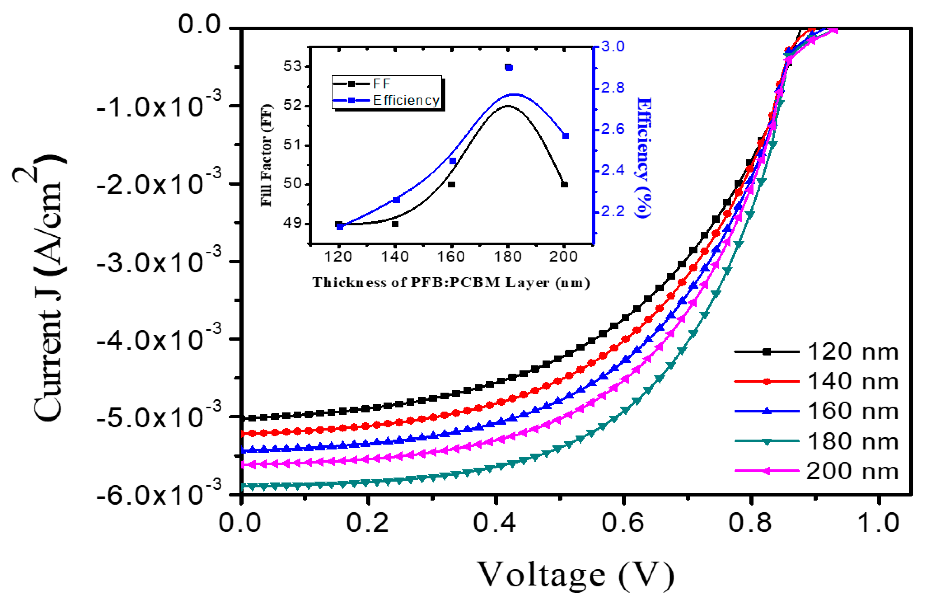
Figure 1. Molecular structures (a) poly(9,9-dioctylfluorenyl-2,7-diyl)-co-(N,N0-diphenyl)-N,Ndi(p-butyl-oxy-pheyl)-1,4-diamino-benzene) (PFB) and (b) [6, 6]-Phenyl-C61-butyric acid methyl ester (PCBM); (c) Device structure of PFB–PCBM blend based bulk heterojunction (BHJ) solar cell; (d) Energy levels diagram of PFB–PCBM device at equilibrium unbiased.
Energies 13 05915 g001
Figure 2. Current–voltage (I-V) characteristics of indium tin oxide (ITO)/ poly(3,4-ethylenedioxythiophene):poly(styrene sulfonate (PEDOT:PSS)/PFB–PCBM)/Ag BHJ solar cells of different thicknesses under illumination at standard testing conditions (STC) inset: active layer thickness vs. efficiency and fill factor (FF) graph.
Energies 13 05915 g002
Figure 3. (a) UV-Vis spectrum; inset: XRD pattern and (b) AFM images of PFB:PCBM blended film.
Energies 13 05915 g003
Figure 4. Current–voltage (I-V) curves of ITO/PEDOT:PSS/PFB–PCBM/Ag BHJ solar cell in dark; inset: (a) The semi-log I-V (b) The log I-log V.
Energies 13 05915 g004
Table 1. Comparison of different parameters of the fabricated BHJ solar cells as a function of PFB–PCBM film thickness.
Sample#Film Thickness (nm)Voc (V)Jsc (mA/cm2)Pmax (mW/cm2)FF (%)PCE (%)
11200.875.02.14492.13
21400.895.22.26492.26
31600.915.42.44502.45
41800.935.92.88532.90
52000.925.62.58502.57
Table 2. Comparison of PCE, VOC, ISC, and FF of a PFB–PCBM-based device with the same device architecture poly(3-hexylthiophene) ((P3HT)–PCBM) at a nearly equal film thickness reported elsewhere [32].
DeviceThickness (nm)PCE (%)VOC (V)JSC (mA/cm2)FF (%)REF
PFB-PCBM160 ± 52.450.915.4050Present Work
P3HT-PCBM155 ± 51.940.5946.5150.2[33]
Thienopyrrole/PCBM622.140.817.330.36[48]
Thienothiophene/PCBM562.390.835.440.53[48]
Publisher’s Note: MDPI stays neutral with regard to jurisdictional claims in published maps and institutional affiliations.

