Article

A Topology Synthetization Method for Single-Phase, Full-Bridge, Transformerless Inverter with Leakage Current Suppression—Part II

1
College of Electrical and Information Engineering, Hunan University, Changsha 410082, China
2
Department of Electrical and Computer Engineering, Queen’s University, Kingston, ON K7L 3N6, Canada
*
Author to whom correspondence should be addressed.
Energies 2020, 13(2), 446; https://doi.org/10.3390/en13020446
Submission received: 23 November 2019 / Revised: 6 January 2020 / Accepted: 7 January 2020 / Published: 16 January 2020

Abstract

:
This paper proposes a topology derivation methodology to achieve small leakage current or zero leakage current for photovoltaic application. The core of the proposed method is a unified topology model and MN principle to show how to derive all possible topologies based on unipolar sinusoidal pulse width modulation (USPWM) and double-frequency USPWM (DFUSPWM). Part II of this paper discusses the topology synthetization method to achieve zero leakage current. Two types of neutral point clamped (NPC) topologies based on USPWM and DFUSPWM are elaborated. Two possible connections for the NPC cell are introduced, and detailed NPC topology derivation procedures are also provided. All existing NPC topologies are derived, and twenty-two new NPC topologies are found based on the new topology derivation methodology for a single-phase, full-bridge, transformerless inverter.

Graphical Abstract

1. Introduction

Photovoltaic (PV) sources have been developed as one of the most promising renewable energy sources, providing clean, reliable, and emission-free energy [1,2]. The single phase, transformerless grid-connected inverter has widely been used throughout the world. Considering the electrical connections between the PV panels and utility grid for transformerless, grid-tied systems [3,4,5], the leakage current generated by the PV parasitic capacitors must be limited in order to meet the safety requirement, such as standards of VDC-AR_N 4015 [6], UL1741 [7], VDE 0126-1-1 [8]. Therefore, small and even zero leakage current in transformerless PV inverter systems are a primary priority for designers.
The leakage current can be limited in full-bridge transformerless inverters if the common mode (CM) voltage is zero [9,10]. Some state-of-the art-topologies, such as the H5 inverter topology [11], as shown in Figure 1a, HERIC [12,13], and H6 inverter topologies [9,14,15,16,17,18,19,20,21,22,23,24,25,26,27,28,29,30,31,32,33,34,35,36,37,38,39,40,41,42,43,44], have been developed from the full-bridge inverter topology. However, there is still a small leakage current as the CM voltage no longer remains constant under parasitic parameter inflection throughout the whole line-frequency (50 Hz or 60 Hz) period. The CM voltage is indeed variable in freewheeling mode because of the potential variation induced by the charging of the switch junction capacitance. The Neutral Point Clamped (NPC) technique is introduced in these topologies to achieve zero leakage current [45,46,47,48,49,50,51,52].
The famous dc-based H5 inverter is adopted as an example to explore the inherent leakage current generation caused by the switch junction capacitors. Figure 2 shows the transient operation of H5 and optimized H5 [53].
During the positive half cycle, switches T1, TP2, and TP3 are turned on, and switches TN2 and TN3 are turned off. Then, switches T1 and TP2 are turned off. Simultaneously, the body-diode of switch TN2 does not conduct to go into freewheel mode. At this moment, junction capacitors CS1 and CP3 are charged while junction capacitors CN2 and CN3 are discharged. The transient charging and discharging operation from the power delivery mode to the freewheeling mode is demonstrated in Figure 2a. The voltage VAN decreases and VBN increases. The body-diode of switch TN2 is conducted to enter the freewheeling mode when the voltage CN2 is lowered to zero.
The equivalent circuit is illustrated in Figure 2b and the voltages VAN and VBN can be derived by (1)
V AN = V BN = C P 3 + C N 3 C S 1 + C P 3 + C N 3 V dc
From (1), the steady-state voltage VAN, VBN is determined by the junction capacitors of the switches. The switch junction capacitors are approximately from several hundred picofarads to several nanofarads. The parasitic capacitor Cpv is around one hundred nanofarads [16,18,45]. If CS1 = CP3 + CN3, the voltages VAN and VBN are both equal to Vdc/2. This indicates that the total high-frequency CM voltage is Vdc/2. Unfortunately, for most industrial applications, CS1 ≠ CP3 + CN3. This means that the total high-frequency CM voltage is not kept constant, which leads to unexpected leakage current. Furthermore, in freewheeling mode, the terminals A and B are floating, and an additional resonant path is formed, which is illustrated in Figure 2b. A high-frequency resonance occurs, which also may lead to the generation of leakage current. The resonance frequency can be calculated by
f r = 1 2 π L eq C eq
where
L eq =   L 1 L 2 L 1 + L 2 ;   C eq =   ( C S 1 +   C P 3 +   C N 3 ) C PV C S 1 +   C P 3 +   C N 3 +   C PV C S 1 +   C P 3 +   C N 3
To clamp the CM voltage to half of the dc-link voltage in freewheeling mode, the bus capacitors are divided into two same-series capacitors, and a clamping cell should be inserted between the midpoint of the series bus capacitors. This can provide a constant CM voltage, which can eliminate the effect of the junction capacitors of the switches. Figure 1b shows the OH5 topology with the NPC cell. Switch TB1 turns on to connect point A (or B) to point O in freewheeling mode. A new circuit configuration for the inverter with a single dc-link capacitor and seven insulated gate bipolar transistors (IGBTs) is proposed in [54]. The additional switch is turned on in the freewheeling modes, and two turn-OFF snubber circuits are added in parallel to the switches in order to share the input dc voltage between the snubber capacitors. As a result, the leakage current can be eliminated completely because the bridge voltages can be clamped at half dc-link voltage in the freewheeling modes. Two neutral point clamping circuits, which are common collectors and common emitters, are proposed in [55], and then a family of single-phase inverters is presented.
In theory, many topologies that could suppress leakage current. Some of them have been studied intensively and patented. However, some may not have been studied or even found. The purpose of this paper is to propose a systematic topology deduction method to obtain all the topologies with the ability to suppress leakage current to zero in theory [56]. Part II of this paper investigates the rules by which to synthesize the two type of NPC topologies to achieve zero leakage current. The first one is called “indirect connection NPC topology”, and the other is called “direct connection NPC topology”. Part II of this paper is organized as follows: Section 2 proposes the rules by which to synthesize the two type of NPC cells. Section 3 introduces two topology families based on indirect connection NPC cells from USPWM. Section 4 provides two topology families based on direct connection NPC cells from USPWM. The proposed topology derivation methodology is also extended to DFUSPWM in Section 5. The simulation results are provided to verify the performance of the proposed topologies in Section 6, and Part II of the paper is concluded in Section 7.

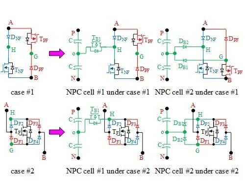
2. NPC Cells for USPWM

To substantially reduce the leakage current, the CM voltage VCM should be clamped to half of the input voltage in freewheeling mode, including in PF and NF modes. Points A and B are short-circuited to achieve VAB = 0 in freewheeling mode. The extra circuit, called “NPC cell”, will be introduced to clamp the CM voltage and achieve zero leakage current. The NPC cell is made of two series capacitors and some additional switches. The DC bus capacitor is split into two identical capacitors, C1 and C2, in series. Due to the participation of the NPC cell, point A (or point B) is connected to midpoint O between C1 and C2, which guarantees that the CM voltage is half of the input voltage in PF mode and NF mode. The terms TPF and TNF are used to refer to the equivalent switch in the freewheeling branch in PF mode and NF mode, respectively. There are two basic rules concerning the NPC cell. Rule 1 is used to make full use of the original freewheeling switching devices in the topology and minimize the number of switches to be added. Rule 2 is used to give the locations where the switching devices of the NPC cell should be added.
Rule #1:
To reduce the number of switches in NPC cell, both TPF and TNF are turned on in freewheeling mode, including in PF and NF modes.
Rule #2:
Additional switches are added and connected to the freewheeling branch so that point A or B is clamped to point O.
Based on Rule #1, it is possible that TNF works for the NPC cell in PF mode, and TPF in NF mode. So, the number of switches needed in the NPC cell is reduced.
Based on Rule #2, two possible connections are available. One is that additional switches are added between point O and a point from the freewheeling branch. This type of connection is defined as an “Indirect Connection”. The other is that additional switches are inserted into the freewheeling branch which is connected to point O due to the injection of additional switches. This type of connection is defined as a “Direct Connection”.
Figure 3 shows the schematic diagram of the Indirect Connection of a unified NPC cell for USPWM.
Two capacitors with the same capacitance value are connected in series to halve the input voltage. Point O is the midpoint of these two capacitors. Additional switches are added between points O and G in Figure 3a and between points O and H in Figure 3b. It should be noted that points G and H are from the freewheeling branch. Figure 3a shows the Indirect Connection in PF mode, which means the actual current flows from point G to point O. Figure 3b shows the NF mode operation, which means that the actual current flows from point O to point H.
Figure 4 shows a schematic diagram of the Direct Connection of the unified NPC cell for USPWM. As shown in Figure 4a, additional switches marked by the green bump branch HI ^ are inserted into the freewheeling branch BCA ^ , so that BCA ^ is connected to the midpoint O. Points H and I are from the freewheeling branch.
Figure 4b shows the NF mode operation. The additional switches marked by the green branch KJ ^ are inserted into the freewheeling branch ADB ^ , and ADB ^ is connected to the midpoint O due to the injection of KJ ^ .

3. Inverter Topologies Based on the Indirect Connection of NPC Cell from USPWM

As with the Indirect Connection of the NPC cell shown in Figure 3 the freewheeling branch is connected directly through additional switches to point O to achieve zero leakage current. Part I of this paper has described the development of all the possible topologies of inverters with low leakage current where the freewheeling branch is not connected to the capacitor midpoint O. The topologies with NPC cells can be derived based on the non-NPC topologies derived in Part I of this paper. There will be one NPC inverter topology corresponding to each non-NPC inverter topology derived in Part I.
This section focuses on how to derive the inverter topologies based on the Indirect Connection of an NPC cell under USPWM. Two topology families from the unified topology model have been described in Part I. One has an extra diode which is used to flow freewheeling current, and the other has no extra diode, but rather, body-diode switch is used to flow freewheeling current. Correspondingly, the inverter topologies with the Indirect Connection NPC cell can also be classified into two families, as shown in Table 1, R1 is a topology without an NPC cell that has been proposed in Part I. R1S1 is the topology with the NPC cell corresponding to R1, and will be examined in this paper.

3.1. Indirect Connection NPC Cell Based on Two Topology Familes
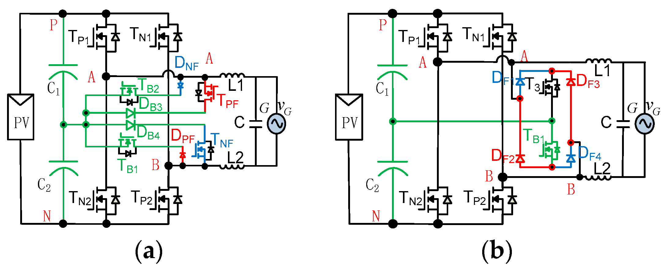
Figure 3 shows the Indirect Connection NPC cell circuits based on the topology family with an extra diode. Two freewheeling cell circuits are introduced, and four corresponding NPC cell circuits are described.
As described in Part I of this paper, there are two freewheeling cell circuits based on the topology family with an extra diode, as shown in Figure 5a,d. For Figure 5a, the current flows from point B to point A through switch TPF and diode DPF in series, and from point A to point B through switch TNF and diode DNF in series. In Figure 5d, the current flows bidirectionally between points B and A through the switch TF, which is kept on in both PF and NF modes.
An extra switch, TB1, is added between points O and H in Figure 5b,e. According to Rule #1, both switches TPF and TNF in Figure 5b are turned on in PF and NF modes. The midpoint O is connected to point B through the extra switch TB1 and switch TNF based on Rule #2. Switches TB1 and TNF are connected in series to realize bidirectional current flow between point O and point B, as shown in Figure 5b. Similarly, the switch TF in Figure 5e is turned on in both PF and NF modes based on Rule #1. The midpoint O is connected to point B through the extra switch TB1 and the switch TF based on Rule #2.
Two extra diodes, DB1 and DB2, are added between points O and H, O and G in Figure 5c,f. Both switches TPF and TNF in Figure 5c are turned on in PF and NF modes based on Rule #1. Point B is connected to point O through diode DB1 and switch TPF or through DB2 and TNF in Figure 5c, based on Rule #2. A bidirectional current branch clamps point B (or point A) in PF mode and NF mode. It is easy to make a similar analysis of the NPC cell shown in Figure 5f. For the sake of brevity, this is not presented here.
As described in Part I of this paper, two methods can be used to construct the freewheeling cell based on the topology family without an extra diode; they are shown in Figure 6a,c. In Figure 6b, the extra switch TB1 is added between points O and G (H), and the midpoint O is connected to point B (or point A) through the extra switch TB1 based on Rule #2. Two extra diodes, DB1 and DB2, are added between points O and G/H in Figure 6d. DB1 and DB2 are used to provide the bidirectional current path in PF and NF modes. The corresponding NPC topologies will be described in the next section.
Figure 6 shows the Indirect Connection NPC cell circuits based on the topology family without an extra diode. Two freewheeling cell circuits are introduced, and two corresponding NPC cell circuits are described.

3.2. M = 2, N = 2

The steps of how to derive the Indirect Connection NPC topology R1S1 based on HERIC topology R1are illustrated in Figure 7.
The HERIC topology, named R1 in Figure 7a, is well known. Points A and B are short-circuited in PF mode (the red branch from point B to A) and NF mode (the blue branch from point A to B). The current flows to point B through TP3, DP3 to Point A in PF mode, and flows point A through TN3, DN3 to point B in NF mode. The DC capacitor Cdc is split into two series capacitors, C1 and C2, to provide half the input voltage shown in Figure 7b,c. According to Rule #1, switches TP3 and TN3 are on. An extra switch TB1 is added so that point B is clamped to point O, as shown in Figure 7b. As shown in Figure 7c, two additional diodes, DB1 and DB2, are added to guarantee that point B is clamped to point O.
Figure 8 shows all the NPC topologies under M = 2, N = 2.
An extra switch, TB1, is added to flow the bidirectional current, as shown in Figure 8a,c,d. Two extra diodes, DB1 and DB2, are added to flow bidirectional current, as shown in Figure 8b,e.

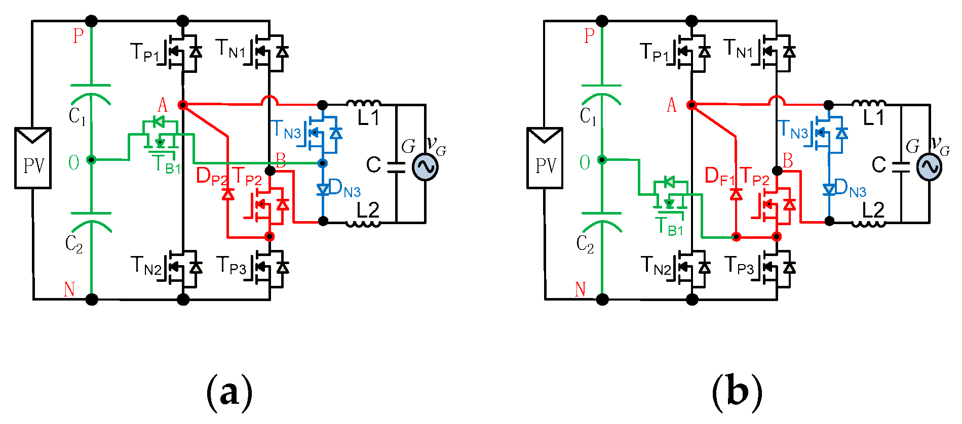
3.3. M = 2, N = 3 or M = 3, N = 2

Figure 9 shows all the NPC topologies under M = 2, N = 3 or M = 3, N = 2. An extra switch, TB1, is added to flow bidirectional current, as shown in Figure 8b and Figure 9a,d. Two extra diodes, DB1 and DB2, are added to flow bidirectional current, as shown in Figure 9c.

3.4. M = 3, N = 3

Figure 10 shows all the NPC topologies based on the original topologies H6 and H5 under M = 3, N = 3.

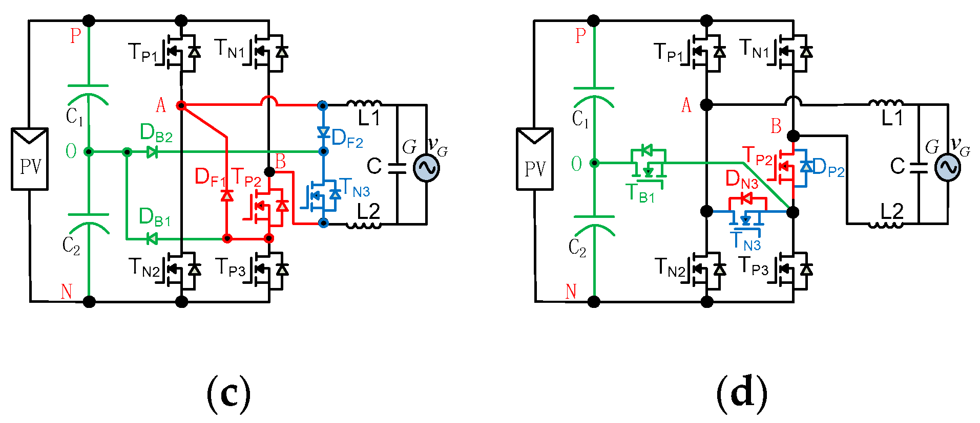
3.5. M = 3, N = 4 or M = 4, N = 3

Figure 11 shows all the NPC topologies under M = 3, N = 4 or M = 4, N = 3.

3.6. M = 4, N = 4

Figure 12 shows all the NPC topologies under M = 4, N = 4.

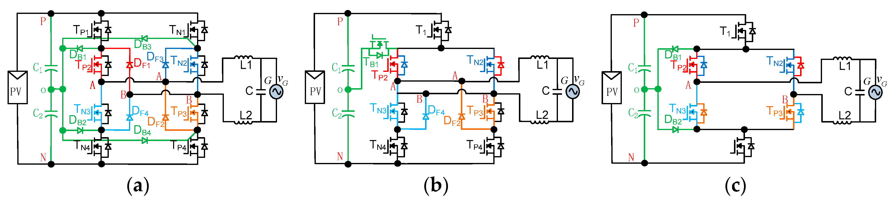
4. Inverter Topologies Based on the Direct Connection NPC Cell from USPWM

In this section, inverter topologies based on a Direct Connection NPC cell from USPWM are introduced. As shown in Table 2, they are also classified into two families.

4.1. Direct Connection NPC Cell Based on Two Topology Families
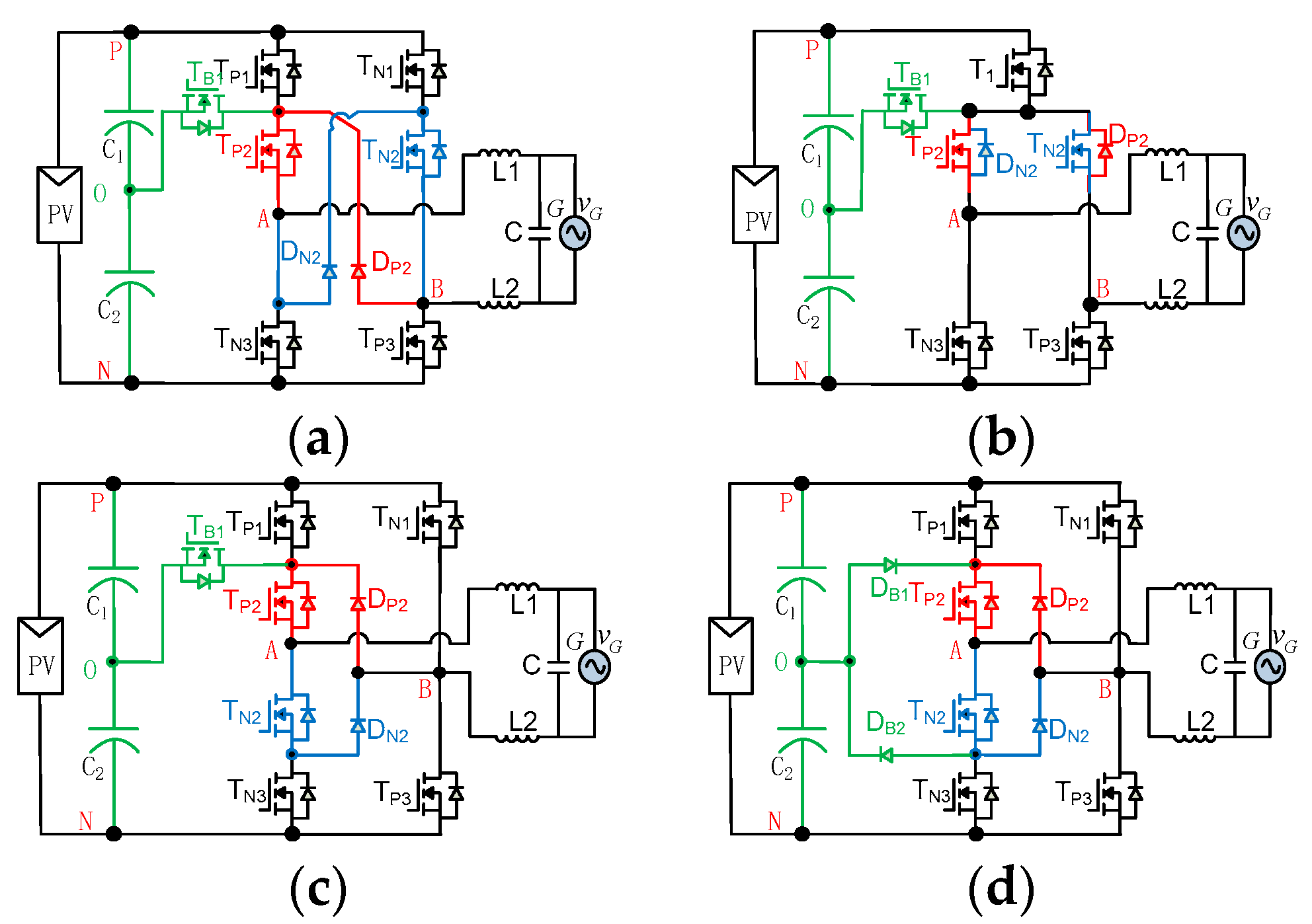
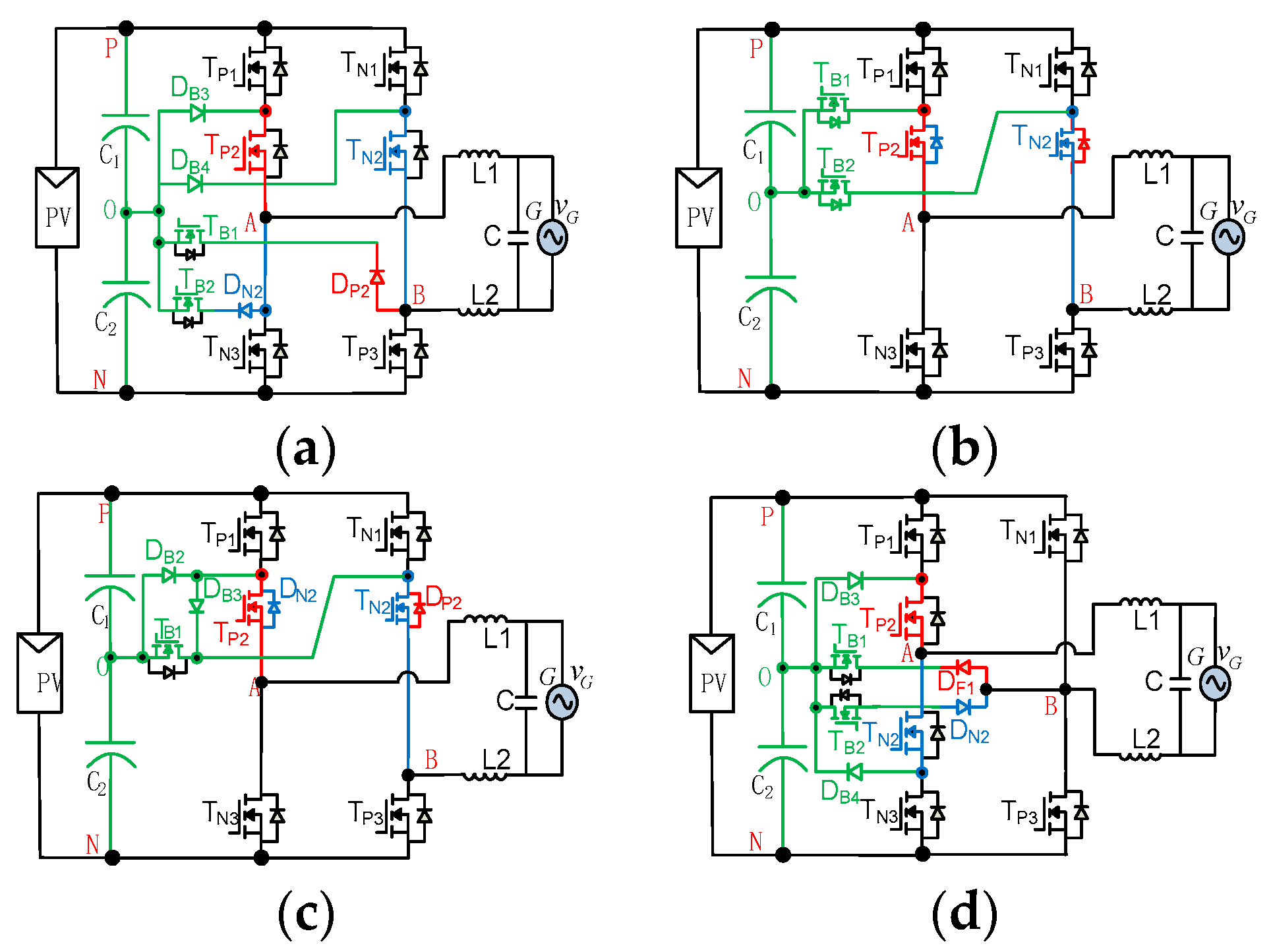
Figure 13 shows the Direct Connection NPC cell circuits based on the topology family with an extra diode. Two freewheeling cell circuits are introduced in Figure 13a,c, respectively. The switches TPF and TNF in the NPC cell are on in both PF and NF mode, based on Rule #1. According to Rule #2, the extra switches, TB1, TB2, and extra diodes, DB3, DB4, are inserted into the freewheeling cell in Figure 13b. As shown in Figure 13b, the midpoint O is connected to point B (or point A) through the extra switch TB1 (TB2) and extra diode DB4 (DB3). The midpoint O is connected to point B through the extra switch TB1 shown in Figure 13d. It is observed that the freewheeling cell is changed due to the injection of extra switches and diodes.
Figure 14 shows the Direct Connection NPC cell circuits based on the topology family without an extra diode. There is one circuit which may be used to construct the freewheeling cell, as shown in Figure 14a. Figure 14b,c show the NPC cell circuits. The original freewheeling branch is cut and two extra switches, TB1 and TB2, are inserted to form the new freewheeling branch Figure 14b. The midpoint O is connected to point B (or point A) through the extra switches TB1 (or TB2) based on Rule #2. One extra switch, TB1, and two extra diodes, DB2 and DB3, are inserted to construct the new freewheeling branch in Figure 14c. The current flows from point B to point A through DPF, TB1, DB2, TPF in PF mode and point B is connected to point O. The current flows from point A to point B through DNF, DB3, and TNF.

4.2. M = 2, N = 2

In order to show how the Direct Connection NPC topology R2S2 is derived based on HERIC topology R2, it is illustrated in Figure 15. According to Rule #1, switches TP3 and TN3 are on in PF and NF modes. As shown in Figure 15b, two extra switches, TB1 and TB2, are inserted so that point B or point A is clamped to point O based on Rule #2. In Figure 15c, two extra diodes, DB2 and DB3, and one extra switch, TB1, are inserted to guarantee that point B is clamped to point O.
Figure 16 shows the other Direct Connection NPC topologies based on HERIC topology under M = 2, N = 2. Two extra switches, TB1 and TB2, are inserted as shown in Figure 16a, and TB1 is inserted in Figure 16b.

4.3. M = 2, N = 3 or M = 3, N = 2

Figure 17 shows all the NPC topologies under M = 2, N = 3 or M = 3, N = 2. Two extra switches, TB1, TB2, and two extra diodes, DB3 and DB4, are inserted so that point B or A is clamped to point O, as shown in Figure 17a. Two extra switches, TB1, TB2, are inserted in Figure 17b. One switch, TB1, and two diodes, DB2 and DB3, are inserted in Figure 17c.

4.4. M = 3, N = 3

Figure 18 shows all the NPC topologies under M = 3, N = 3. Two extra switches, TB1 and TB2, and two extra diodes, DB3 and DB4, are inserted in Figure 18a,d. Two extra switches, TB1, TB2, are added in Figure 18b. One switch, TB1, and two diodes, DB2, DB3, are added in Figure 18c.

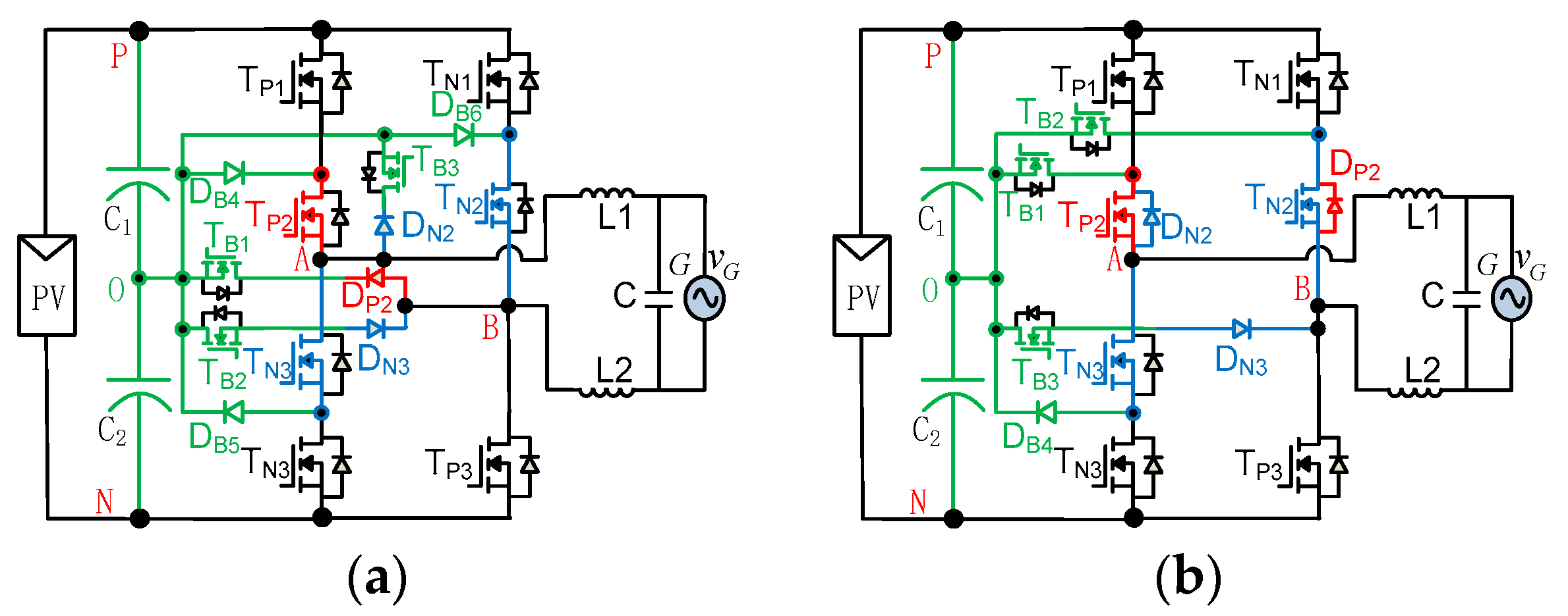
4.5. M = 3, N = 4 or M = 4, N = 3
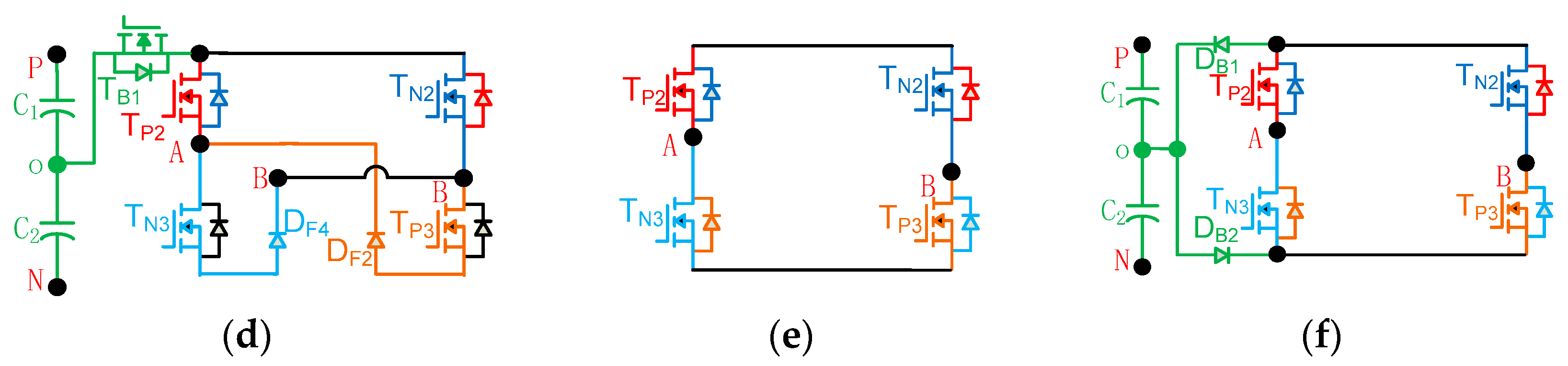
Figure 19 shows the NPC topologies under M = 3, N = 4 or M = 4, N = 3.

4.6. M = 4, N = 4

Figure 20 shows all the NPC topologies under M = 4, N = 4. Figure 20a is given as an example to describe the current flowing. In PF or NF mode, there are two branches for the flow of positive current. One is as follows: Point B→DP2→TB1→DB5→TP2→Point A, and the other is from Point B→TP3→DB6→TB2→DP3→Point A. Similarly, there are two branches for the flow of negative current. The first one is as follows: Point A→DN2→TB3→DB7→TN2→Point B. The other is from Point A→TN3→DB8→TB4→DN3→Point B.

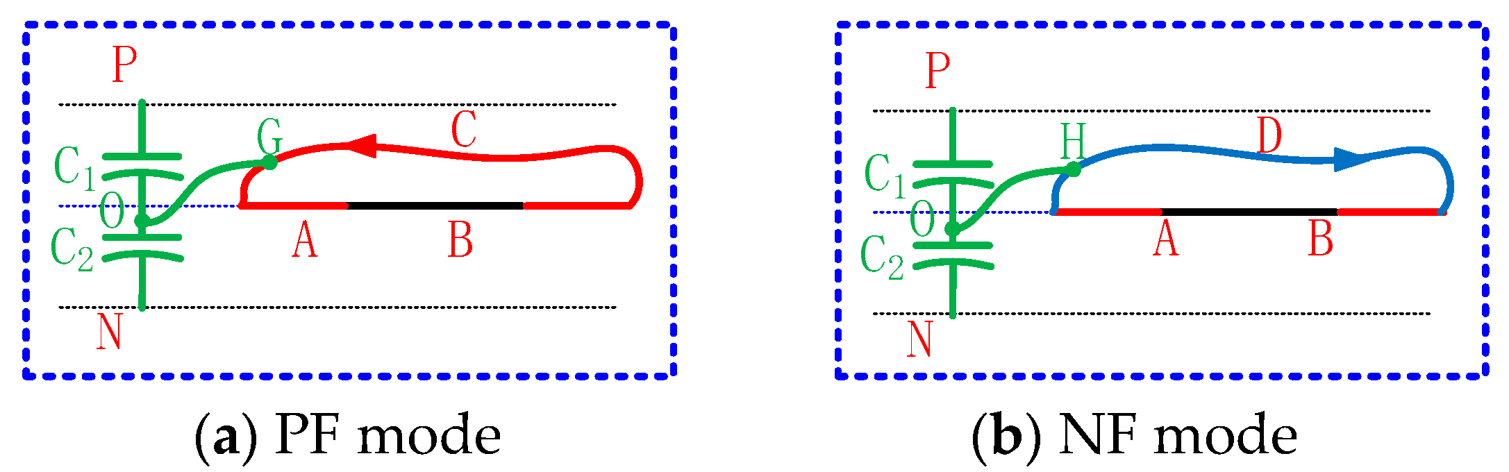
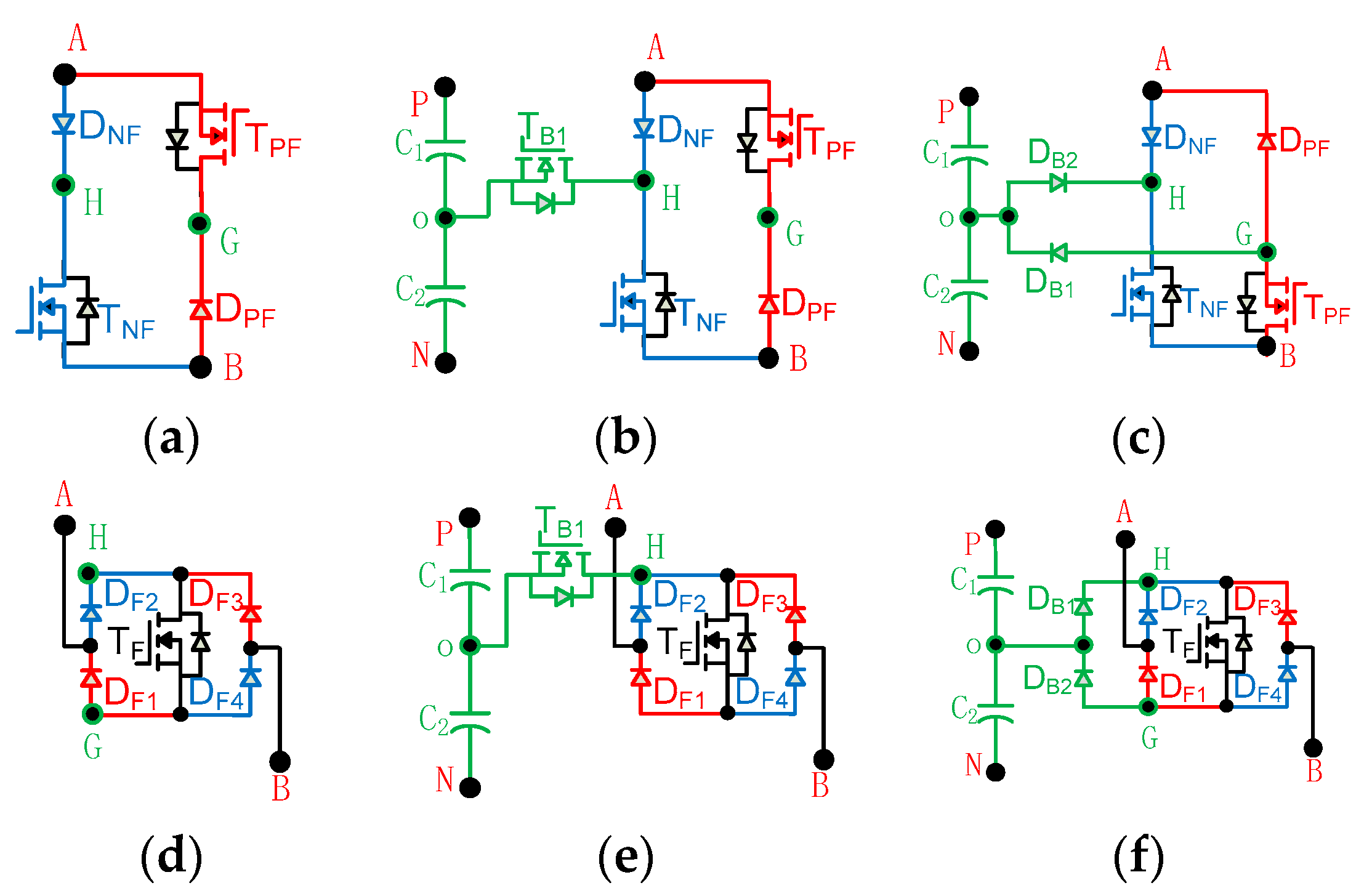
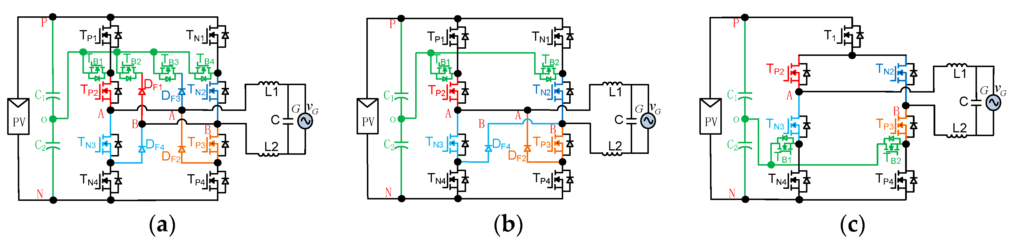
5. Two Types of NPC Cells and Reflected Topologies under DFUSPWM

Similar to USPWM, there are two type of NPC cells under DFUSPWM. Part A introduces the principle of the Indirect Connection NPC cell and reflected topologies under DFUSPWM. Part B introduces the principle of the Direct Connection NPC cell and reflected topologies under DFUSPWM.

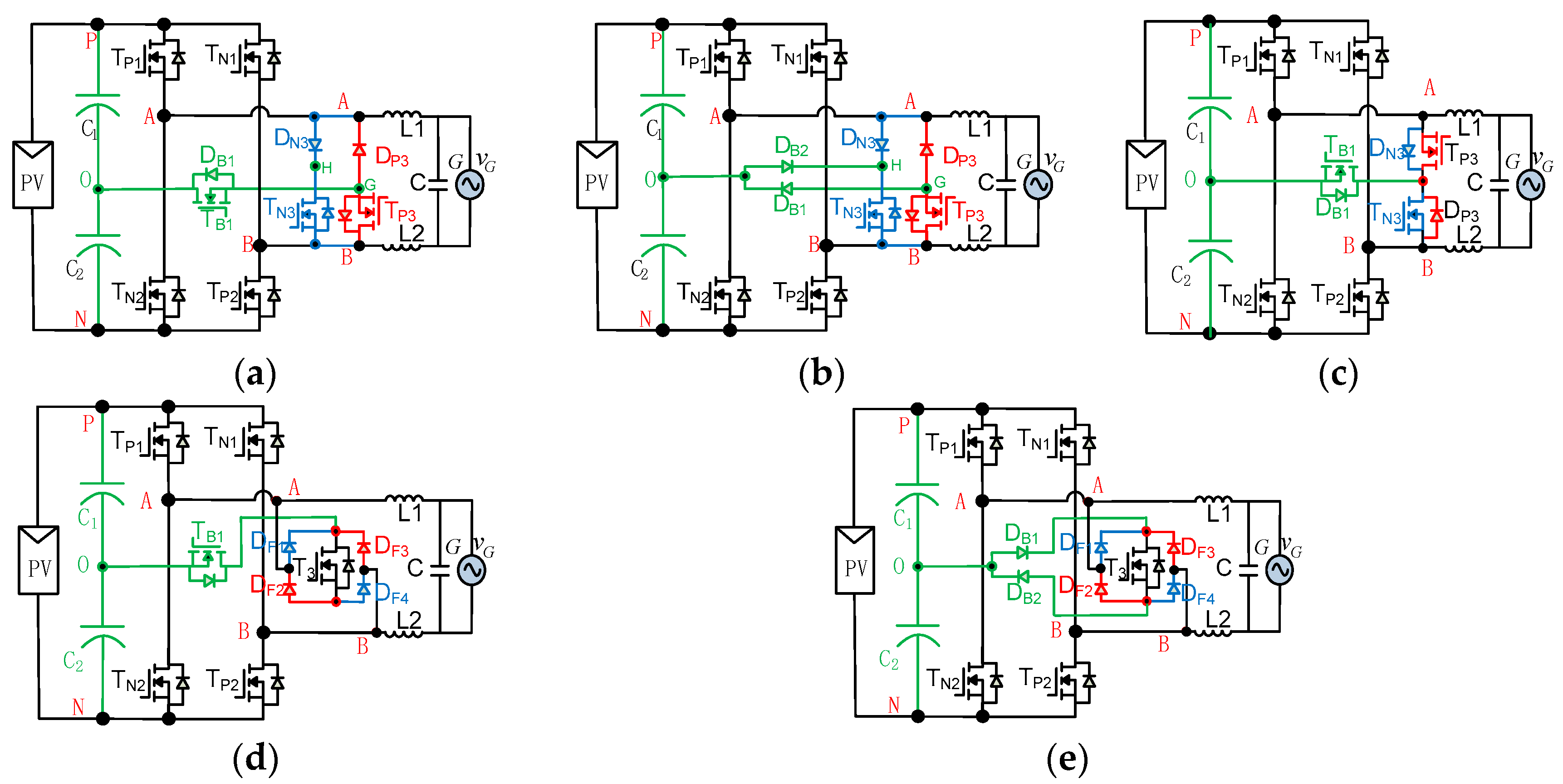
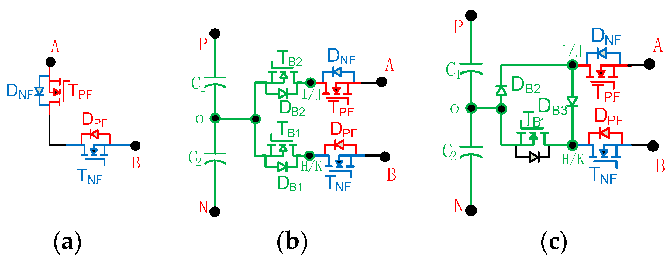
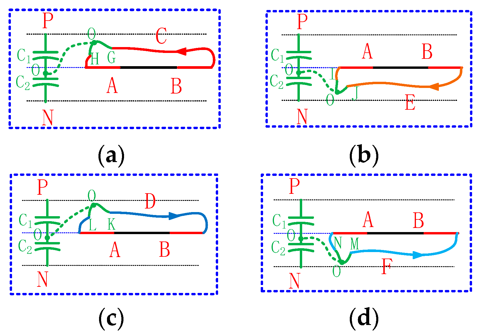
5.1. Principle of Indirect Connection NPC Cell and Reflected Topologies under DFUSPWM

Figure 21 shows a schematic diagram of the first type of unified NPC cell. Two capacitors with the same capacitance are connected in series to achieve half of the input voltage for each one. The Indirect Connection NPC cell under DFUSPWM is connected to the freewheeling cell through extra branches in PFT mode, PFB mode, NFT mode, and NFB mode to keep the CM voltage constant. The extra branches are OG ^ and OH ^ flowing positive current in Figure 21a,b, and OI ^ and OJ ^ flowing negative current in Figure 21c,d. It can be seen that the internal connections of the freewheeling cell remain the same in freewheeling mode.
The inverter topologies with the Indirect Connection NPC cell under DFUSPWM can also be classified into two types, as shown in Table 3.
Figure 22 shows the Indirect Connection NPC cell circuits based on freewheeling cell circuits. There are three methods by which to construct the freewheeling cell based on the topology family with an extra diode. They are shown respectively in Figure 5a and Figure 22c,e.
For the NPC cells in Figure 22b,d,f, TP2 and TN3 have the same signals to remain on or off, and TP3 and TN2 have the same driving signals under DFUSPWM. Thus, additional diodes or switches can be used to provide a bidirectional current branch to clamp point A or point B to point O. The corresponding inverter topologies are shown in Figure 23.

5.2. Principle of the Direct Connection NPC Cell and Reflected Topology under DFUSPWM

Figure 24 shows a schematic diagram of the second type of unified NPC cell under DFUSPWM. The extra branch GH ^ is injected into the freewheeling path BCA ^ in Figure 24a, and IJ ^ is injected into the freewheeling path BEA ^ in Figure 24b. Similarly, the extra branch KL ^ is injected into the freewheeling path ADB ^ in Figure 24c and MN ^ is injected into the freewheeling path AFB ^ in Figure 24d. Clearly, the internal connections of the freewheeling cell have been changed due to the injection of the Direct Connection NPC cell.
The inverter topologies with the Direct Connection NPC cell under DFUSPWM can also be classified into two types, as shown in Table 4.
Figure 25 shows the Direct Connection NPC cell circuits based on the freewheeling cell circuits under DFUSPWM. Three freewheeling cell circuits are introduced in Figure 25a,c,e.
There are two current branches which allow the current to flow from point B to A, or from point A to B. Point A is of the same voltage as point B so that point A or point B is connected to NPC cell.
For NPC cells, as shown in Figure 25b,d,f, additional diodes and/or switches are used to provide a bidirectional current branch to clamp point A or B to point O. The corresponding inverter topologies are shown in Figure 26.
In order to make an overall comparison of all the derived topologies, Table 5 and Table 6 are presented, wherein the number of switches, the number of diodes and the economic cost of all the derived topologies are taken into consideration. Among them, the economic cost part is obtained based on the formula that each switch costs 1, while each diode costs 0.3. Based on the two tables, we may select a circuit topology which is suitable for our situation.

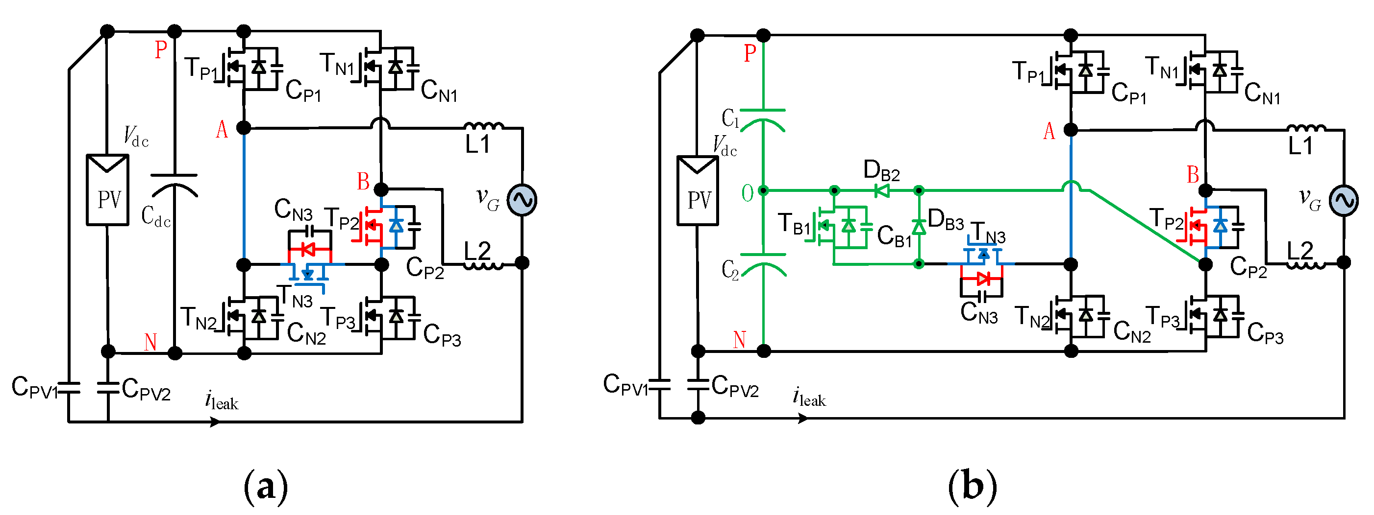
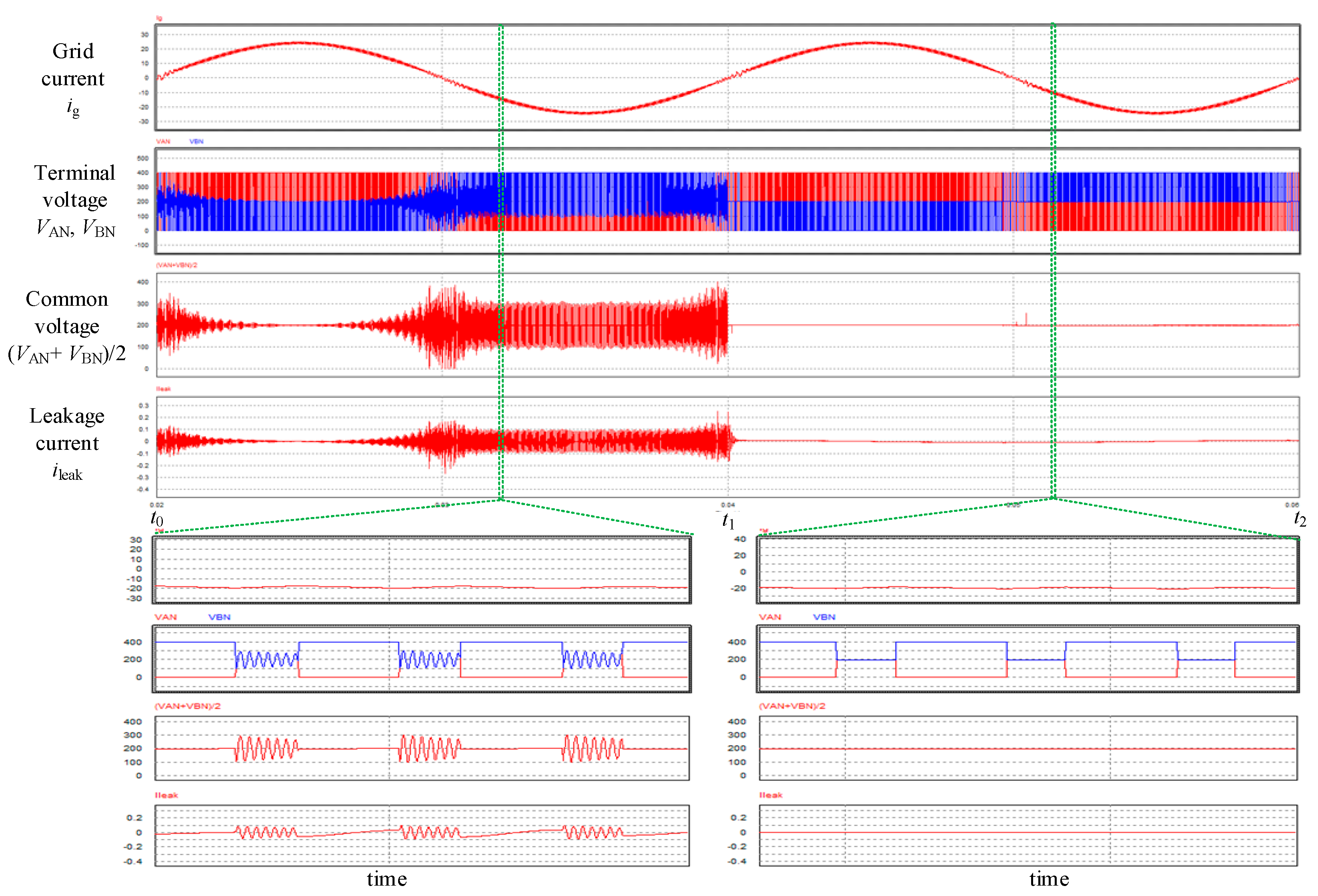
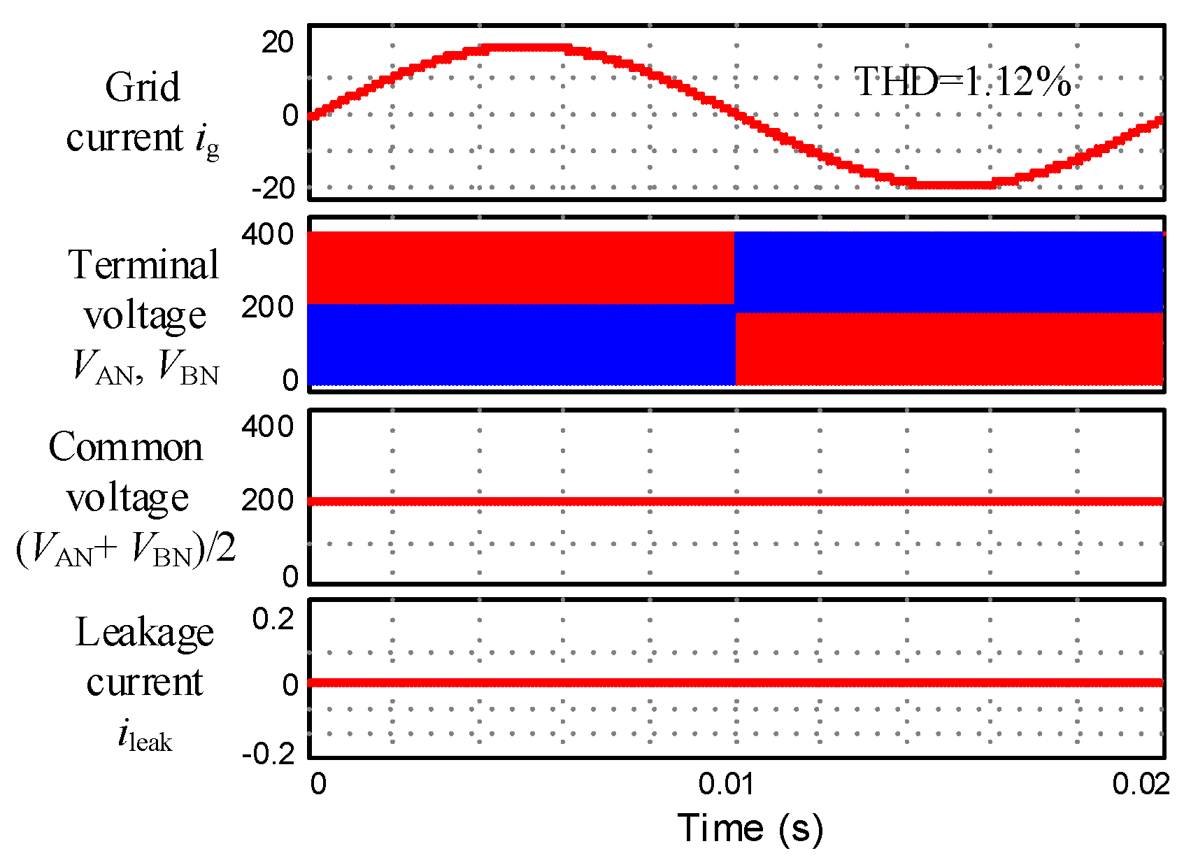
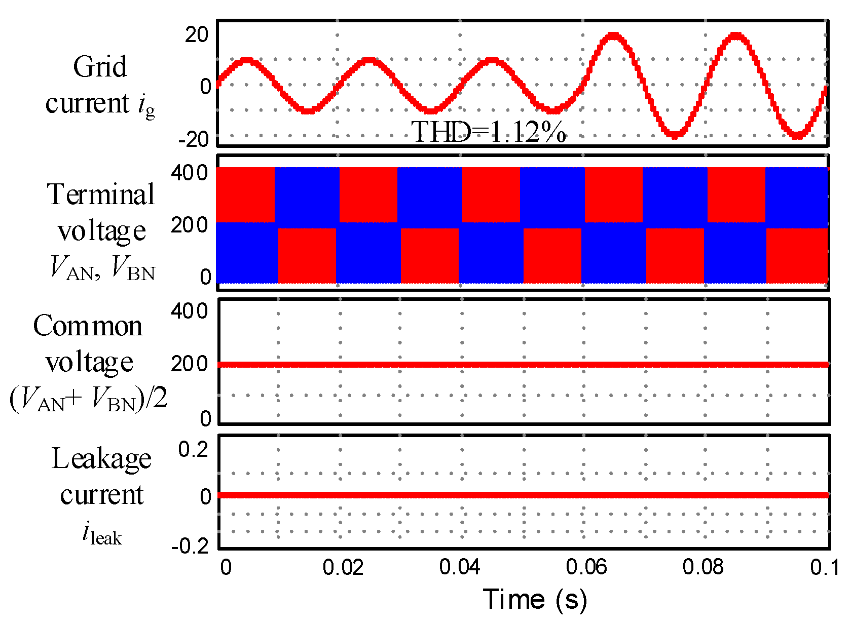
6. Simulation Results

Two types NPC topologies with a Direct Connection NPC cell or an Indirect Connection NPC cell are provided based on the topologies provided in Part I of this paper. To further verify the theoretical analysis in the coming sections, simulations based on two proposed topologies are made, and the simulation results are given. One is the H6 topology (R5) and the proposed H6 topology with a Direct Connection NPC cell (R5S2-2) under USPWM. The other is the proposed H8 topology (R13) and H8 topology with an Indirect Connection NPC cell (R11S1) under DFUSPWM. 0shows the simulation parameters.

6.1. H6 Topology Without/With Direct Connection NPC Cell under USPWM

Figure 27 shows the H6 topology without/with a Direct Connection NPC cell. The H6 topology R5 is illustrated in Figure 27a. Switches TP2 and TN3 are used to allow the freewheeling current to flow. The freewheeling branch is cut off and the Direct Connection NPC cell is injected into the topology R5 to form R5S2-2, as shown in Figure 27b.
Figure 28 shows the waveforms of CM voltage and leakage current. In t0t1, the topology H6 without the NPC cell works, and the CM voltage (VAN + VBN)/2 does not remain constant. The CM voltage includes high frequency resonant voltage in freewheeling mode, as terminals A and B are floating (VAN = VBN). The leakage current is 100 mA. In t1t2, the topology H6 with the NPC cell works and the CM voltage (VAN + VBN)/2 always remains constant. The leakage current is reduced from 100 mA to 2 mA.
Figure 29 shows the waveforms of the grid current, terminal voltage, CM voltage, and leakage current with the parameters listed in Table 7. The THD of the grid current is about 1.12%. As we can see, the CM voltage is maintained at 200 V with small fluctuations over the whole power line period; thus, the RMS value of the leakage current is only 3 mA. Figure 30 shows the waveforms when the load steps at t = 0.06 s. The THD is still 1.12%. The CM voltage and leakage current have the same values as those in Figure 29.

6.2. H8 Topology Without/With Indirect Connection NPC Cell under DFUSPWM

Figure 31 shows the topology H8 without/with “Indirect Connection” NPC cell under DFUSPWM.
Figure 32 shows the waveforms of CM voltage and leakage current. It may be observed that the topology H8 without the NPC cell works, and the CM voltage is not constant between t0 and t1. The CM voltage contains high frequency resonant voltage in freewheeling mode due to the floating terminals A and B. The leakage current is 100 mA. In t1t2, the topology H8 with NPC cell works, and the CM voltage always remains constant. The leakage current is reduced from 100 mA to 3 mA.
Figure 33 shows the waveforms of the leakage current, voltage VAB, and PWM signal. The same PWM signals are provided to couple switches TP1 and TP3, TP2 and TP4, TN1 and TN3, as well as TN2 and TN4. To achieve good clamping performance, complementary PWM signals are given to couple switches TP1 and TN2, as well as TP2 and TN1. The frequency of voltage VAB is double the switching frequency.

7. Conclusions

In this paper, a topology derivation methodology, named the “MN principle”, is proposed to cover all possible full-bridge topologies with leakage current suppression under USPWM and DFUSPWM. Two types of NPC cells have been developed: one is called “indirect connection NPC topology”, and the other “direct connection NPC topology”. Under USPWM, twenty-three newly-found indirect connection NPC topologies have been derived along with the existing ones, and twenty-two newly-found direct connection NPC topologies have been derived along with the existing ones. The proposed method is also extended to the topologies under DFUSPWM. As a result, four corresponding topologies have been derived and one existing topology was also covered. Finally, simulations are given to verify the performance of the leakage current suppression of the proposed topologies. And it can be inferred that the contribution of this paper has important guiding significance for topological derivation.

Author Contributions

Conceptualization, X.Y., X.W.; funding acquisition, X.W.; investigation, X.Y.; software, X.Z.; validation, X.Z., X.W.; writing—original draft, X.Y.; writing—review and editing, H.W. and Y.-F.L. All authors have read and agreed to the published version of the manuscript.

Funding

Research on Topology, Passive Current Sharing Mechanism and Control for Multiphase Resonant Converter with Coupled Resonant Tank: 51977069; Research on High-power and High-efficiency Electro-acoustic Transduction Mechanism and Control Method: 51837005.

Conflicts of Interest

The authors declare no conflict of interest.

References

  1. Sun, K.; Zhang, L.; Xing, Y.; Guerrero, J.M. A Distributed Control Strategy Based on DC Bus Signaling for Modular Photovoltaic Generation Systems With Battery Energy Storage. IEEE Trans. Power Electron. 2011, 26, 3032–3045. [Google Scholar] [CrossRef] [Green Version]
  2. EPIA. Global Market Outlook for Photovoltaics 2013–2017; European Photovoltaic Industry Association: Brussels, Belgium, 2013. [Google Scholar]
  3. Kjaer, S.B.; Pedersen, J.K.; Blaabjerg, F. A review of single-phase grid-connected inverters for photovoltaic modules. IEEE Trans. Ind. Appl. 2005, 41, 1292–1306. [Google Scholar] [CrossRef]
  4. Blaabjerg, F.; Zhe, C.; Kjaer, S.B. Power electronics as efficient interface in dispersed power generation systems. IEEE Trans. Power Electron. 2004, 19, 1184–1194. [Google Scholar] [CrossRef]
  5. Quan, L.; Wolfs, P. A Review of the Single Phase Photovoltaic Module Integrated Converter Topologies With Three Different DC Link Configurations. IEEE Trans. Power Electron. 2008, 23, 1320–1333. [Google Scholar] [CrossRef] [Green Version]
  6. Power Generation Systems Connected to the Low-Voltage Distribution Network, VDE-AR-N 4105. Available online: https://www.sogou.com/link?url=hedJjaC291MdqKRdyYP6xaEfyF6gLPTmC2Ly98cd-IVBavtdX5bT4M0N-aB7Vy-zp32izvdhNQ_l-ZZN6CSHZQ (accessed on 1 August 2011).
  7. Standard for Inverters, Converters, Controllers, and Interconnection System Equipment for Use With Distributed Energy Resources. Available online: https://standardscatalog.ul.com/standards/en/standard_1741_2 (accessed on 28 January 2010).
  8. Automatic Disconnection Device Between a Generator and the Public Low-Voltage Grid, DIN VDE V 0126-1-1. Available online: https://www.beuth.de/en/pre-standard/din-vde-v-0126-1-1/187485608 (accessed on 1 August 2013).
  9. Gonzalez, R.; Gubia, E.; Lopez, J.; Marroyo, L. Transformerless Single-Phase Multilevel-Based Photovoltaic Inverter. IEEE Trans. Ind. Electron. 2008, 55, 2694–2702. [Google Scholar] [CrossRef]
  10. Xiao, H.; Xie, S. Transformerless Split-Inductor Neutral Point Clamped Three-Level PV Grid-Connected Inverter. IEEE Trans. Power Electron. 2012, 27, 1799–1808. [Google Scholar] [CrossRef]
  11. Victor, M.; Greizer, K.; Bremicker, A. Method of Converting a Direct Current Voltage from a Source of direct Current Voltage, More Specifically from a Photovotatic Source of Direct Current Voltage, into a Alternating Current Voltage. U.S. Patent 7411802B2, 12 August 2008. [Google Scholar]
  12. Schmidt, H.; Siedle, C.; Ketterer, J. Inverter for Converting an Electric Direct Current into an Alternating Current or an Alternating Voltage. European Patent EP2 086 102 A2, 5 August 2009. [Google Scholar]
  13. Patino, D.G.; Erira, E.G.; Fuelagan, J.R.; Rosero, E.E. Implementation a HERIC inverter prototype connected to the grid controlled by SOGI-FLL. In Proceedings of the 2015 IEEE Workshop on Power Electronics and Power Quality Applications (PEPQA), Bogota, Colombia, 2–4 June 2015; pp. 1–6. [Google Scholar]
  14. Zhang, L.; Sun, K.; Xing, Y.; Xing, M. H6 Transformerless Full-Bridge PV Grid-Tied Inverters. IEEE Trans. Power Electron. 2014, 29, 1229–1238. [Google Scholar] [CrossRef]
  15. Yu, W.; Jai, J.-S.; Qian, H.; Hutchens, C.; Zhang, J.; Lisi, G.; Djabbari, A.; Smith, G.; Hegarty, T. High-efficiency inverter with H6-type configuration for photovoltaic non-isolated ac module applications. In Proceedings of the 2010 Twenty-Fifth Annual IEEE Applied Power Electronics Conference and Exposition (APEC), Palm Springs, CA, USA, 21–25 February 2010; pp. 1056–1061. [Google Scholar]
  16. Yang, B.; Li, W.; Gu, Y.; Cui, W.; He, X. Improved Transformerless Inverter With Common-Mode Leakage Current Elimination for a Photovoltaic Grid-Connected Power System. IEEE Trans. Power Electron. 2012, 27, 752–762. [Google Scholar] [CrossRef]
  17. Su, X.; Sun, Y.; Lin, Y. Analysis on Leakage Current in Transformerless Single-Phase PV Inverters Connected to the Grid. In Proceedings of the 2011 Asia-Pacific Power and Energy Engineering Conference (APPEEC), Wuhan, China, 25–28 March 2011; pp. 1–5. [Google Scholar]
  18. Xiao, H.F.; Ke, L.; Li, Z. A Quasi-Unipolar SPWM Full-Bridge Transformerless PV Grid-Connected Inverter with Constant Common-Mode Voltage. IEEE Trans. Power Electron. 2015, 30, 3122–3132. [Google Scholar] [CrossRef]
  19. Xiao, H.; Xie, S.; Chen, Y.; Huang, R. An Optimized Transformerless Photovoltaic Grid-Connected Inverter. IEEE Trans. Ind. Electron. 2011, 58, 1887–1895. [Google Scholar] [CrossRef]
  20. Wang, J.; Ji, B.; Zhao, J.; Yu, J. From H4, H5 to H6 Standardization of full-bridge single phase photovoltaic inverter topologies without ground leakage current issue. In Proceedings of the 2012 IEEE Energy Conversion Congress and Exposition (ECCE), Raleigh, NC, USA, 15–20 September 2012; pp. 2419–2425. [Google Scholar]
  21. Vazquez, G.; Martinez-Rodriguez, P.R.; Sosa, J.M.; Escobar, G.; Juarez, M.A. Transformerless single-phase multilevel inverter for grid tied photovoltaic systems. In Proceedings of the IECON 2014—40th Annual Conference of the IEEE Industrial Electronics Society, Dallas, TX, USA, 29 October–1 November 2014; pp. 1868–1874. [Google Scholar]
  22. Vazquez, G.; Martinez-Rodriguez, P.R.; Sosa, J.M.; Escobar, G.; Arau, J. A modulation strategy for single-phase HB-CMI to reduce leakage ground current in transformer-less PV applications. In Proceedings of the IECON 2013—39th Annual Conference of the IEEE Industrial Electronics Society, Vienna, Austria, 10–13 November 2013; pp. 210–215. [Google Scholar]
  23. Figueredo, R.S.; de Carvalho, K.C.M.; Ama, N.R.N.; Matakas, L. Leakage current minimization techniques for single-phase transformerless grid-connected PV inverters—An overview. In Proceedings of the 2013 Brazilian Power Electronics Conference (COBEP), Gramado, Brazil, 27–31 October 2013; pp. 517–524. [Google Scholar]
  24. Hu, S.; Cui, W.; Li, W.; He, X.; Cao, F. A high-efficiency single-phase inverter for transformerless photovoltaic grid-connection. In Proceedings of the 2014 IEEE Energy Conversion Congress and Exposition (ECCE), Pittsburgh, PA, USA, 14–18 September 2014; pp. 4232–4236. [Google Scholar]
  25. Salmon, J.; Knight, A.; Ewanchuk, J. Single phase multi-level PWM Inverter topologies using coupled inductors. In Proceedings of the 2008 IEEE Power Electronics Specialists Conference (PESC), Rhodes, Greece, 15–19 June 2008; pp. 802–808. [Google Scholar]
  26. Ozkan, Z.; Hava, A.M. Leakage current analysis of grid connected transformerless solar inverters with zero vector isolation. In Proceedings of the 2011 IEEE Energy Conversion Congress and Exposition (ECCE), Phoenix, AZ, USA, 17–22 September 2011; pp. 2460–2466. [Google Scholar]
  27. Lopez, O.; Teodorescu, R.; Freijedo, F.; DovalGandoy, J. Leakage current evaluation of a singlephase transformerless PV inverter connected to the grid. In Proceedings of the APEC 2007—Twenty Second Annual IEEE Applied Power Electronics Conference and Exposition, Anaheim, CA, USA, 25 February–1 March 2007; pp. 907–912. [Google Scholar]
  28. Ma, L.; Tang, F.; Zhou, F.; Jin, X.; Tong, Y. Leakage current analysis of a single-phase transformer-less PV inverter connected to the grid. In Proceedings of the 2008 IEEE International Conference on Sustainable Energy Technologies (ICSET), Singapore, 24–27 November 2008; pp. 285–289. [Google Scholar]
  29. Kerekes, T.; Teodorescu, R.; Rodriguez, P.; Vazquez, G.; Aldabas, E. A New High-Efficiency Single-Phase Transformerless PV Inverter Topology. IEEE Trans. Ind. Electron. 2011, 58, 184–191. [Google Scholar] [CrossRef] [Green Version]
  30. Ji, B.; Wang, J.; Zhao, J. High-Efficiency Single-Phase Transformerless PV H6 Inverter With Hybrid Modulation Method. IEEE Trans. Ind. Electron. 2013, 60, 2104–2115. [Google Scholar] [CrossRef]
  31. Islam, M.; Mekhilef, S. A new high efficient transformerless inverter for single phase grid-tied photovoltaic system with reactive power control. In Proceedings of the 2015 IEEE Applied Power Electronics Conference and Exposition (APEC), Charlotte, NC, USA, 15–19 March 2015; pp. 1666–1671. [Google Scholar]
  32. Islam, M.; Mekhilef, S. High efficiency transformerless MOSFET inverter for grid-tied photovoltaic system. In Proceedings of the 2014 Twenty-Ninth Annual IEEE Applied Power Electronics Conference and Exposition (APEC), Fort Worth, TX, USA, 16–20 March 2014; pp. 3356–3361. [Google Scholar]
  33. San, G.; Qi, H.; Wu, J.; Guo, X. A new three-level six-switch topology for transformerless photovoltaic systems. In Proceedings of the 2012 7th International Power Electronics and Motion Control Conference (IPEMC), Harbin, China, 2–5 June 2012; pp. 163–166. [Google Scholar]
  34. Freddy, T.K.S.; Rahim, N.A.; Wooi-Ping, H.; Che, H.S. Comparison and Analysis of Single-Phase Transformerless Grid-Connected PV Inverters. IEEE Trans. Power Electron. 2014, 29, 5358–5369. [Google Scholar] [CrossRef]
  35. Du, D.; Hao, R.; Li, H.; Zheng, T.Q. A novel H6 topology and Its modulation strategy for transformerless photovoltaic grid-connected inverters. In Proceedings of the 2014 16th European Conference on Power Electronics and Applications (EPE’14-ECCE Europe), Lappeenranta, Finland, 26–28 August 2014; pp. 1–8. [Google Scholar]
  36. Dong, D.; Luo, F.; Boroyevich, D.; Mattavelli, P. Leakage Current Reduction in a Single-Phase Bidirectional AC-DC Full-Bridge Inverter. IEEE Trans. Power Electron. 2012, 27, 4281–4291. [Google Scholar] [CrossRef]
  37. Cui, W.; Yang, B.; Zhao, Y.; Li, W.; He, X. A novel single-phase transformerless grid-connected inverter. In Proceedings of the IECON 2011—37th Annual Conference on IEEE Industrial Electronics Society, Melbourne, VIC, Australia, 7–10 November 2011; pp. 1126–1130. [Google Scholar]
  38. Gu, B.; Dominic, J.; Lai, J.-S.; Chen, C.-L.; LaBella, T.; Chen, B. High Reliability and Efficiency Single-Phase Transformerless Inverter for Grid-Connected Photovoltaic Systems. IEEE Trans. Power Electron. 2013, 28, 2235–2245. [Google Scholar] [CrossRef]
  39. Gu, B.; Dominic, J.; Chen, B.; Lai, J.-S. A high-efficiency single-phase bidirectional AC-DC converter with miniminized common mode voltages for battery energy storage systems. In Proceedings of the 2013 IEEE Energy Conversion Congress and Exposition (ECCE), Denver, CO, USA, 15–19 September 2013; pp. 5145–5149. [Google Scholar]
  40. Basu, K.; Mohan, N. A High-Frequency Link Single-Stage PWM Inverter With Common-Mode Voltage Suppression and Source-Based Commutation of Leakage Energy. IEEE Trans. Power Electron. 2014, 29, 3907–3918. [Google Scholar] [CrossRef]
  41. Barater, D.; Buticchi, G.; Crinto, A.S.; Franceschini, G.; Lorenzani, E. Unipolar PWM Strategy for Transformerless PV Grid-Connected Converters. IEEE Trans. Energy Convers. 2012, 27, 835–843. [Google Scholar] [CrossRef]
  42. Barater, D.; Buticchi, G.; Crinto, A.S.; Franceschini, G.; Lorenzani, E. A new proposal for ground leakage current reduction in transformerless grid-connected converters for photovoltaic plants. In Proceedings of the 2009 35th Annual Conference of IEEE Industrial Electronics (IECON’09), Porto, Portugal, 3–5 November 2009; pp. 4531–4536. [Google Scholar]
  43. Islam, M.; Afrin, N.; Mekhilef, S. Efficient single phase transformerless inverter for grid-tied PVG system with reactive power control. IEEE Trans. Sustain. Energy 2016, 7, 1205–1215. [Google Scholar] [CrossRef]
  44. Islam, M.; Mekhilef, S. H6-type transformerless single-phase inverter for grid-tied photovoltaic system. IET Power Electron. 2015, 8, 636–644. [Google Scholar] [CrossRef] [Green Version]
  45. Anandababu, C.; Fernandes, B.G. Improved full-bridge neutral point clamped transformerless inverter for photovoltaic grid-connected system. In Proceedings of the IECON 2013—39th Annual Conference of the IEEE Industrial Electronics Society, Vienna, Austria, 10–13 November 2013; pp. 7996–8001. [Google Scholar]
  46. Anandababu, C.; Fernandes, B.G. A novel neutral point clamped transformerless inverter for grid-connected photovoltaic system. In Proceedings of the IECON 2013—39th Annual Conference of the IEEE Industrial Electronics Society, Vienna, Austria, 10–13 November 2013; pp. 6962–6967. [Google Scholar]
  47. Zhang, L.; Sun, K.; Feng, L.; Wu, H.; Xing, Y. A Family of Neutral Point Clamped Full-Bridge Topologies for Transformerless Photovoltaic Grid-Tied Inverters. IEEE Trans. Power Electron. 2013, 28, 730–739. [Google Scholar] [CrossRef]
  48. Duan, S.; Liu, B.; Kang, Y. A Single-phase Hybrid-Bridge Three-Level Inverter. Chinese Patent ZL200910063079.1, 14 September 2011. [Google Scholar]
  49. Gonzalez, R.; Lopez, J.; Sanchis, P.; Marroyo, L. Transformerless Inverter for Single-Phase Photovoltaic Systems. IEEE Trans. Power Electron. 2007, 22, 693–697. [Google Scholar] [CrossRef]
  50. Li, W.; Gu, Y.; Luo, H.; Cui, W.; He, X.; Xia, C. Topology Review and Derivation Methodology of Single-Phase Transformerless Photovoltaic Inverters for Leakage Current Suppression. IEEE Trans. Ind. Electron. 2015, 62, 4537–4551. [Google Scholar] [CrossRef]
  51. Zhou, L.; Gao, F.; Yang, T. Neutral-point-clamped circuits of single-phase PV inverters: Generalized principle and implementation. In Proceedings of the 2015 IEEE Energy Conversion Congress and Exposition (ECCE), Montreal, QC, Canada, 20–24 September 2015; pp. 442–449. [Google Scholar]
  52. Islam, M.; Mekhilef, S. Efficient transformerless MOSFET inverter for a grid-tied photovoltaic system. IEEE Trans. Power Electron. 2016, 31, 6305–6316. [Google Scholar] [CrossRef]
  53. Mei, Y.; Hu, S.; Lin, L.; Li, W.; He, X.; Cao, F. Highly efficient and reliable inverter concept-based transformerless photovoltaic inverters with tri-direction clamping cell for leakage current elimination. IET Power Electron. 2016, 9, 1675–1683. [Google Scholar] [CrossRef]
  54. Akpınar, E.; Balıkcı, A.; Durbaba, E.; Azizoğlu, B.T. Single-phase transformerless photovoltaic inverter with suppressing resonance in improved H6. IEEE Trans. Power Electron. 2019, 34, 8304–8316. [Google Scholar] [CrossRef]
  55. Zhou, L.; Gao, F. Low leakage current single-phase PV inverters with universal neutral-point-clamping method. In Proceedings of the 2016 IEEE Applied Power Electronics Conference and Exposition (APEC), Long Beach, CA, USA, 20–24 March 2016; pp. 410–416. [Google Scholar]
  56. Wang, H.; Burton, S.; Liu, Y.-F.; Sen, P.C.; Guerrero, J.M. A systematic method to synthesize new transformerless full-bridge grid-tied inverters. In Proceedings of the 2014 IEEE Energy Conversion Congress and Exposition (ECCE), Pittsburgh, PA, USA, 14–18 September 2014; pp. 2760–2766. [Google Scholar]
Figure 1. H5 topology without/with NPC cell. (a) H5 topology [11]; (b) Optimized H5 (OH5) [19].
Energies 13 00446 g001
Figure 2. Transient charging and discharging operation of H5. (a) Transient operation [53]; (b) Equivalent circuit [53].
Energies 13 00446 g002
Figure 3. Indirect Connection of Unified NPC cell under USPWM. (a) PF mode; (b) NF mode.
Energies 13 00446 g003
Figure 4. Direct Connection of Unified NPC cell under USPWM. (a) PF mode; (b) NF mode.
Energies 13 00446 g004
Figure 5. Indirect Connection NPC cell circuits based on topology family with an extra diode. (a) case #1; (b) NPC cell #1 under case #1; (c) NPC cell #2 under case #1; (d) case #2; (e) NPC cell #1 under case #2; (f) NPC cell #2 under case #2.
Energies 13 00446 g005
Figure 6. Indirect Connection of NPC cell circuits based on topology family without an extra diode. (a) case #1; (b) NPC cell #1 under case #1; (c) case #2; (d) NPC cell under case #2.
Energies 13 00446 g006
Figure 7. Indirect Connection NPC topologies R1S1 under M = 2, N = 2. (a) HERIC topology R1; (b) R1S1-1; (c) R1S1-2 [50,51].
Energies 13 00446 g007
Figure 8. Indirect Connection NPC topologies from M = 2, N = 2. (a) R1S1-1 [50]; (b) R1S1-2 [18,50,51]; (c) R2S1 [51]; (d) R3S1-1 [51]; (e) R3S1-2 [51].
Energies 13 00446 g008
Figure 9. Indirect Connection NPC topologies from M = 2, N = 3 or M = 3, N = 2. (a) R4S1-1 [51]; (b) R4S1-2 [51]; (c) R4S1-3 [51]; (d) R5S1 [50].
Energies 13 00446 g009aEnergies 13 00446 g009b
Figure 10. Indirect Connection NPC topologies from M = 3, N = 3. (a) R6S1 [51]; (b) R7S1 [19]; (c) R8S1-1 [51]; (d) R8S1-2 [48].
Energies 13 00446 g010
Figure 11. Indirect Connection NPC topologies from M = 3, N = 4 or M = 4, N = 3. (a) R9S1-1 (new); (b) R9S1-2 (new); (c) R10S1 (new).
Energies 13 00446 g011
Figure 12. Indirect Connection NPC topologies from M = 4, N = 4. (a) R11S1-1 (new); (b) R11S1-2 (new); (c) R12S1-1 (new); (d) R12S1-2 (new); (e) R13S1-1 [49]; (f) R13S1-2 [49].
Energies 13 00446 g012
Figure 13. Direct Connection NPC cell circuits based on topology family with an extra diode. (a) Case #1; (b) NPC cell under case #1; (c) Case #2; (d) NPC cell under case #2 (new).
Energies 13 00446 g013
Figure 14. Direct Connection NPC cell circuits based on topology family without an extra diode. (a) freewheeling circuit; (b) NPC cell #1; (c) NPC cell #2.
Energies 13 00446 g014
Figure 15. Direct Connection NPC topologies R1S2 under M = 2, N = 2. (a) HERIC topology R2; (b) R2S2-1 from R2; (c) R2S2-2 from R2 (new).
Energies 13 00446 g015
Figure 16. Direct Connection NPC topologies from M = 2, N = 2. (a) R1S2 (new); (b) R3S2 (new).
Energies 13 00446 g016
Figure 17. Direct Connection NPC topologies from M = 2, N = 2. (a) R4S2 (new); (b) R5S2-1 [47]; (c) R5S2-2 (new).
Energies 13 00446 g017
Figure 18. Direct Connection NPC topologies from M = 3, N = 3. (a) R6S2 (new); (b) R7S2-1 [47]; (c) R7S2-2 (new); (d) R8S2 (new).
Energies 13 00446 g018
Figure 19. Direct Connection NPC topologies from M = 3, N = 3. (a) R9S2 (new); (b) R10S2 (new).
Energies 13 00446 g019
Figure 20. Direct Connection NPC topologies from M = 4, N = 4. (a) R11S2 (new); (b) R12S2 (new); (c) R13S2 (new).
Energies 13 00446 g020
Figure 21. Indirect Connection NPC cell under DFUSPWM. (a) PFT mode; (b) PFB mode; (c) NFT mode; (d) NFB mode.
Energies 13 00446 g021
Figure 22. Indirect Connection NPC cell circuits under DFUSPWM. (a) case #1; (b) NPC cell under case #1; (c) case #2; (d) NPC cell under case #2; (e) case #3; (f) NPC cell under case #3.
Energies 13 00446 g022aEnergies 13 00446 g022b
Figure 23. Inverter topologies with the Direct Connection NPC cell under DFUSPWM. (a) R11S1 (new); (b) R12S1 (new); (c) R13S1 (new).
Energies 13 00446 g023
Figure 24. Direct Connection NPC cell under DFUSPWM. (a) PFT mode; (b) PFB mode; (c) NFT mode; (d) NFB mode.
Energies 13 00446 g024
Figure 25. Direct Connection NPC cell circuits under DFUSPWM. (a) case #1; (b) NPC cell under case #1; (c) case #2; (d) NPC cell under case #2; (e) case #3; (f) NPC cell under case #3.
Energies 13 00446 g025
Figure 26. Inverter topologies with the Direct Connection NPC cell under DFUSPWM. (a) R11S2 (new); (b) R12S2 (new); (c) R13S2 (new).
Energies 13 00446 g026
Figure 27. Topology H6 without /with NPC cell under USPWM. (a) R5; (b) R5S2-2 (new).
Energies 13 00446 g027
Figure 28. Waveforms of grid current, terminal voltage, CM voltage, and leakage current.
Energies 13 00446 g028
Figure 29. Waveforms of grid current, terminal voltage, CM voltage, and leakage current.
Energies 13 00446 g029
Figure 30. Waveforms of grid current, terminal voltage, CM voltage, and leakage current in the case.
Energies 13 00446 g030
Figure 31. Topology H8 without /with NPC cell under DFUSPWM. (a) R13 (new); (b) R11S1 (new).
Energies 13 00446 g031
Figure 32. Waveforms of grid current, terminal voltage, CM voltage and leakage current.
Energies 13 00446 g032
Figure 33. Waveforms of leakage current, voltage VAB, and PWM signal.
Energies 13 00446 g033
Table 1. Two inverter topology families from USPWM.
(M, N)X1 + X2Y1 + Y2Family With Extra DiodeFamily Without Extra Diode
Without NPC Cell (Part I)With NPC Cell (Part II)Without NPC Cell (Part I)With NPC Cell (Part II)
(M = 2, N = 2)1 + 11 + 1R1, R3R1S1-1,
R1S1-2, R3S1-1,
R3S1-2
R2R2S1
(M = 2, N = 3)
or
(M = 3, N = 2)
1 + 21 + 1R4R4S1-1,
R4S1-2,
R4S1-3
R5R5S1
1 + 11 + 2
2 + 11 + 1
1 + 12 + 1
(M = 3, N = 3)2 + 12 + 1R6R6S1R7R7S1
1 + 21 + 2
2 + 11 + 2R8R8S1-1,
R8S1-2
None availableNone available
1 + 22 + 1
(M = 3, N = 4)
or
(M = 4, N = 3)
1 + 22 + 2R9R9S1-1,
R9S1-2
R10R10S1
2 + 21 + 2
2 + 12 + 2
2 + 22 + 1
(M = 4, N = 4)2 + 22 + 2R11, R12R11S1-1,
R11S1-2, R12S1-1,
R12S1-2
R13R13S1-1,
R13S1-2
Table 2. Two inverter topology families from USPWM.
(M, N)X1 + X2Y1 + Y2Family With Extra DiodeFamily Without Extra Diode
Without NPC Cell (Part I)With NPC Cell (Part II)Without NPC Cell (Part I)With NPC Cell (Part II)
(M = 2, N = 2)1 + 11 + 1R1, R3R1S2, R3S2R2R2S2-1,
R2S2-2
(M = 2, N = 3)
or
(M = 3, N = 2)
1 + 21 + 1R4R4S2R5R5S2-1,
R5S2-2
1 + 11 + 2
2 + 11 + 1
1 + 12 + 1
(M = 3, N = 3)2 + 12 + 1R6R6S2R7R7S2-1,
R7S2-2
1 + 21 + 2
2 + 11 + 2R8R8S2None availableR8S2
1 + 22 + 1
(M = 3, N = 4)
or
(M = 4, N = 3)
1 + 22 + 2R9R9S2R10R10S2
2 + 21 + 2
2 + 12 + 2
2 + 22 + 1
(M = 4, N = 4)2 + 22 + 2R11, R12R11S2, R12S2R13R13S2
Table 3. Two NPC topology families under DFUSPWM.
(M, N)X1 + X2Y1 + Y2Family With Extra DiodeFamily Without Extra Diode
Without NPC CellWith NPC CellWithout NPC CellWith NPC Cell
(M = 4, N = 4)2 + 22 + 2R11, R12R11S1, R12S1R13R13S1
Table 4. Direction connection NPC cell under DFUSPWM.
(M, N)X1 + X2Y1 + Y2Family with Extra DiodeFamily Without Extra Diode
Without NPC CellWith NPC CellWithout NPC CellWith NPC Cell
(M = 4, N = 4)2 + 22 + 2R11, R12R11S2, R12S2R13R13S2
Table 5. Comparison of the Inverter topologies under USPWM.
Topology NameNumber of SwitchesNumber of DiodesEconomic CostTopology NameNumber of SwitchesNumber of DiodesEconomic Cost
R1S1-1727.6R10S1838.9
R1S1-2647.2R13S1-1707
R3S1-1647.2R13S1-2626.6
R3S1-2566.8R1S2849.2
R4S1-1727.6R3S2647.2
R4S1-2727.6R4S2849.2
R4S1-3647.2R6S2849.2
R6S1727.6R8S2849.2
R8S1-1727.6R9S210611.8
R8S1-2647.2R11S212814.4
R9S1-1838.9R12S212413.2
R9S1-2758.5R2S2-1808
R11S1-19410.2R2S2-2727.6
R11S1-2869.8R5S2-1808
R12S1-1828.6R5S2-2828.6
R12S1-2748.2R7S2-1808
R2S1707R7S2-2727.6
R5S1707R10S210210.6
R7S1606R13S212012
Table 6. Comparison of the Inverter topologies under DFUSPWM.
Connection Mode of NPC CellTopologies NameNumber of SwitchesNumber of DiodesEconomic Cost
Indirect ConnectionR11S18810.4
R12S1828.6
R13S1626.6
Direct ConnectionR11S212413.2
R12S210210.6
R13S2909
Table 7. Simulation Parameters.
ParameterValue
Rated power3000 W
Input voltage400 V
Grid voltage/frequency220 V/50 Hz
Filter inductor L1, L21 mH
Switching frequency20 kHz
DC-bus Capacitor Cdc1, Cdc2470 µF
Junction capacitor of each switch100 pF
PV parasitic capacitor CPV1, CPV20.1 µH

