Article

The Enhanced Average Model of the Smart Transformer with the Wye-Delta Connection of Dual Active Bridges

Department of Electrical Engineering, Warsaw University of Technology, 00-662 Warsaw, Poland
*
Author to whom correspondence should be addressed.
Energies 2020, 13(18), 4613; https://doi.org/10.3390/en13184613
Submission received: 14 July 2020 / Revised: 26 August 2020 / Accepted: 31 August 2020 / Published: 4 September 2020
(This article belongs to the Special Issue Control and Topologies of Grid Connected Converters)

Abstract

:
Nowadays, many power electronics converters (PECs) are connected to the distribution grid, increasing the energy quality requirements in point of common coupling (PCC). One of the promising solutions to improve the energy quality is a smart transformer (ST) characterised by additional benefits in relation to the classical transformer throughout the possibility to implement advanced functionalities in PCC. However, the ST contains a lot of power semiconductor switches, making a problem for simulation software and the computer hardware when the control algorithm and all the ST functionalities are investigated. Usually, the solver algorithms in simulation software are used to create many linear time-varying states spaces, which increases exponentially with the number of switches. Therefore, very important is a model averaging process of the selected advanced ST topology, which is the aim of the paper. The proposed ST average model is compared with full switching models of each ST power conversion stage. It allows for decreasing the simulation time a dozen times, enabling the control algorithm analysis with a full ST model. The proposed solution and results prove steady-state and dynamic behaviour of the average model and provide a comprehensive averaging process for a novel multiple active bridge direct current/direct current (DC/DC) converter inside the ST.

Graphical Abstract

1. Introduction

The transformer is one of the most important devices in transmission and distribution grids. Thanks to the dynamic development of a novel semiconductor devices, communication and control systems, as well as intelligent and self-controlled microgrids (smartgrids), a new solution of the transformer has been developed. In the beginning, the idea of Solid-State Transformer (SST) has been presented in [1,2,3]. The main concept of SST is shown in Figure 1. It consists of alternating current-medium voltage/direct current-medium voltage (AC-MV/DC-MV), isolated direct current-medium voltage/direct current-low voltage (DC-MV/DC-LV) and direct current-low voltage/alternating current-low voltage (DC-LV/AC-LV) power electronics converters. It is characterised by several advantages, like high power density, high efficiency, better power quality and control ability [3,4]. In the era of dynamic growth of semiconductor power switches and microcontrollers, the SST has begun more and more advanced and possible to use in the real power system. Taking into consideration many different control solutions for the power electronics converters and communication abilities, the SST idea has evolved into the Smart Transformer (ST).
The ST is characterised by many additional functionalities in relation to the classical transformer (CT), which is not able to support the grid without any auxiliary devices, for example, current harmonics compensation, reactive power compensations, currents symmetrisation [3,5]. The structure of ST can be different, depending on needs and application [6,7,8]. One of the ST classifications is based on the available DC-links with different voltage levels (MV, LV), providing a point of common coupling for auxiliary DC loads, renewable energy sources and the local DC microgrids. Each power conversion stage consists of different power electronics converter’s structures depending on the application (single H-bridges, modular multilevel converters, cascaded converters, T-type converters, etc.). The most advanced topologies include dozens of semiconductor switches or even more than a hundred elements for high power applications. Additionally, a crucial part of the ST is a high-frequency (HF) transformer. Depending on the application and power electronics converters included in the ST, the significantly different HF transformers are designed and used [2,6,9]. Such an advanced power electronics device is a challenge in simulation research, caused by many switching elements, making the simulated circuit strongly non-linear. The simulation software (e.g., PLECS) creates a linear time-varying (LTV) state space associated with all signals in the model in Equation (1).
x ˙ = A σ x + B σ u y = C σ x + D σ u
The index σ means that the software creates a set of state-space matrices for each possible state change of switching elements (Appendix A). Therefore, the circuit is represented by numbers of linear time-invariant (LTI) models. Furthermore, an additional observer makes decisions whether changing the LTI state space is necessary. It allows obtaining the linear and time-invariant model for each switch state permutation. Moreover, it efficiently determines the output vector y. However, on the other hand, that method makes many state-space permutations equal to two to the power of n, where n is the total number of switching elements. That means the number of modes grows exponentially with the numbers of switches in the circuit, which requires a lot of memory, computing power and time.
To conduct an efficient analysis of the advanced power electronics devices, such as the ST, a good practice is the design of an average signal model for the analysed circuit [4,10,11]. It is characterised by the controlled voltage and current sources, which replaces all switching elements. As a result, the simulation can be performed for dozens of power electronics converters, taking into consideration a complex control algorithm and significantly decreasing the simulation time in comparison to the full switching model. The average model design technics are well known in the literature for single power electronic converters included in all ST power stages (AC/DC, DC/DC, DC/AC) [4,10,11,12,13,14,15]. The simple ST average model has also been proposed in the literature, where the DC/DC dual-active bridge (DAB) converter has been replaced by controlled sources and AC/DC and DC/AC converters have been replaced by ideal transformer models [4,12]. That solution focuses mainly on the analysis of the DAB control algorithms, which is the most important part of the ST due to the included HF transformer.
In this paper, a more advanced average model of the ST is proposed, taking into consideration all dynamic behaviours of the real devices, neglecting only switching frequency influences on the measured voltage and currents. The ST is composed of more than a hundred transistors and diodes (Figure 2). The average models of AC-MV/DC-MV side and DC-LV/AC-LV side power electronics converters are investigated and described in Section 2. The crucial part of the ST, the isolated DC-MV/DC-LV converter average model with wye-delta HF transformer, has been proposed as well. In Section 3, the implemented basic control algorithms have been presented (without advanced functionalities of ST) and the simulation results have been shown and compared with the full switching model of each ST power stage as well as the whole device. In the end, the discussion has been included in Section 4.

2. Average Model of the ST

Each topology of the ST can be split into power conversion stages, which usually are defined by different voltage levels and types (AC, DC). Based on the knowledge of the average models of single power electronics converters, the whole ST average structure may be composed of average models of every single converter.

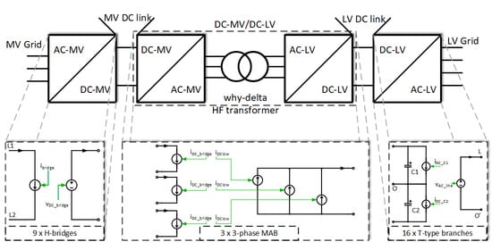
2.1. Model of the AC-MV/DC-MV Side of ST

The considered model of the AC-MV/DC-MV side of ST is a cascaded H-bridge converter (CHBC) composed of nine modules, as it is presented in Figure 1. Due to wye-delta connected dual active bridges in the next conversion stage of the ST, there is no possibility to replace the whole CHBC phase leg by the average model, because all nine DC-links are used (Figure 2). Therefore, each of the H-bridge must be averaging. The single module including four transistors and diodes is replaced by a controlled voltage source (CVS) from the AC converter side and a controlled current source (CCS) from the DC side (Figure 3) [16,17,18]. Taking into consideration the pulse width modulation technique (PWM) in each switching cycle, the voltage vAC is equal to:
v A C = D × v D C
where D—is a modulation index from a range <−1, 1>. This relation determines the control signal directly for the CVS in the average model. The converter DC-side represented by the CCS is derived using the principle of power balance. Assuming, that all the losses in the averaged H-bridge model are not relevant to the control algorithm and may be omitted, the power on the DC side pDC is equal to the power on the AC side pAC:
p A C = v A C i A C = v D C i D C = p D C
Using that relation, the referenced current value for CCS is obtained, as:
i D C = v A C i A C v D C
From (2) and (4), the current of CCS is equal:
i D C = D × i A C

2.2. Model of the Isolated DC-DC Converter with Wye-Delta Transformer

The isolated DC-DC converter based on a dual-active bridge (DAB) is a common solution for bi-directional energy transfer between different DC systems (e.g., energy storage, isolated photovoltaic (PV) systems) [17,19]. The scheme of DAB is shown in Figure 4a. In past years, the DAB topologies have been deeply developed. The basic topology of two H-bridges connected through a one-phase high-frequency transformer has been reorganised with multilevel converters [9,17,20], a resonant circuit for soft-switching ability [21], and multiple active bridge (MAB) converters with wye-wye, delta-delta or wye-delta transformers [9]. The advanced MAB topologies allow operating with higher voltage levels and transformer ratios, a higher efficiency, a higher power of the converter and post-fault mode. Moreover, the MAB advantages are characterised by lower transistor currents, higher phase-shift control ability, lower current ripples in the DC-links and thanks to the wye-delta high-frequency transformer it can operate with unbalanced loads [9].
The modelled ST topology includes three MAB converters (Figure 2), described in [9]. It simplifies the construction of the ST and improves the maintenance due to power electronics building blocks construction (PEBB). MAB can easily work in a post-fault mode of operation, allowing to replace the damaged module. The high-frequency (HF) transformers second windings inside the MAB are connected to the three-phase converter, reducing the current ripples and voltage fluctuations in the DC-link. In developing the average model of that topology, besides the DAB structure, the implemented control solution must be considered. The most common option is a phase shift control, with the constant switching frequency and 50% duty cycle of the rectangular pulses [13,19]. Neglecting the losses of the converter and the HF transformer, the power of the single DAB converter controlled by the phase-shift ϕ is equal to:
P =   v D C _ H i g h v D C _ L o w 2 m f s L e q π ϕ   ( π     ϕ )
where ϕ—phase shift between high frequency voltages vAC_High and vAC_Low (Figure 4a), fs—switching frequency, Leq—equivalent leakage inductance referred to the transformer primary side (Figure 4b).
Two common methods of DAB converter averaging have been taken into consideration to implement them in the proposed DC-DC converter topology. One uses the first harmonic approximation (FHA) [13]. Its main assumption is to use only the first harmonic of two rectangular signals and then adequately rescale the amplitudes of them to obtain the same power flow as for a given phase shift. This approach is characterised by easy implementation and shortens time of simulation, but its disadvantage is a difference in detailed and average model dynamics and the necessity of the additional amplitude value correction for the first harmonic signals to receive the same power flow as for the phase shift control.
Therefore, a more precise solution has been used and described. It is based on the DAB averaging with included values of the high-frequency transformer winding resistances Rp, Rs and leakage inductances Lp, Ls as well as the transistor’s conduction resistance Rc [22]. The equivalent leakage inductance Leq referred to the primary side of the transformer can be calculated as:
L e q =   L p + L s m 2
where Lp—inductance of primary winding, Ls—inductance of secondary winding, m—transformer turn ratio.
The equivalent resistance Req is equal to:
R e q =   R p + 2 R c + R s + 2 R c m 2
where Rp—resistance of primary winding, Rs—resistance of the secondary winding, Rc—the conduction resistance of the transistor.
The average model of the considered isolated DC-DC converter is possible to realise with two current sources as a building block of the whole structure (Figure 5). Knowing the measured values of both DC links voltages and equivalent impedance of the DAB’s internal circuit, the average currents iDC_High and iDC_Low can be calculated as [22]:
i D C H i g h =   ( v D C H i g h + v D C L o w ) d T + ( v D C H i g h v D C L o w ) ( 1 d ) T T R e q + L e q ( i p e a k 1 + v D C H i g h + v D C L o w R e q ) ( e R e q L e q d T 1 ) T R e q + L e q ( v D C _ H i g h v D C _ L o w R e q i p e a k 2 ) ( e R e q L e q ( 1 d ) T 1 ) T R e q
i D C L o w = ( v D C H i g h + v D C L o w ) d T + ( v D C H i g h v D C L o w ) ( 1 d ) T m T R e q L e q ( i p e a k 1 + v D C H i g h + v D C L o w R e q ) ( e R e q L e q d T 1 ) m T R e q + L e q ( v D C _ H i g h v D C _ L o w R e q i p e a k 2 ) ( e R e q L e q ( 1 d ) T 1 ) m T R e q
where T—HF transformer current period presented in Figure 6 (half of a switching period Ts), d—phase shift ratio:
d = ϕ π
v’DC_Low—is a secondary winding voltage referred to the primary side:
v D C _ L o w = v D C _ L o w m
In the reference currents calculation process, two HF transformer current parameters are needed. First, the value of current peak ipeak_1 and the value of current peak ipeak_2 when the current pulse is ending, both presented in Figure 6. Those values are equal to:
i p e a k _ 1 =   v D C _ H i g h v D C _ L o w + 2 v D C _ L o w e R e q L e q ( 1 d ) T R e q ( 1 + e R e q L e q T )   ( v D C _ H i g h + v D C _ L o w ) e R e q L e q T R e q ( 1 + e R e q L e q T )
i p e a k _ 2 =   v D C _ H i g h + v D C _ L o w 2 v D C _ H i g h e R e q L e q d T R e q ( 1 + e R e q L e q T ) +   ( v D C _ H i g h v D C _ L o w ) e R e q L e q T R e q ( 1 + e R e q L e q T )
Using the described model of the single DAB, the MAB DC-DC converter can be modelled based on the scheme presented in Figure 4b. Using three models of that converter, the whole isolated DC-DC stage of the ST shown in Figure 1 is averaged.

2.3. Model of the DC-LV/AC-LV Side of ST

The considered DC-LV/AC-LV stage of the ST consists of four power electronics converter modules connected in parallel as it is shown in Figure 7, providing redundancy and post-fault operation in the device [9]. Each module is composed of a four-leg T-type converter (Figure 7b), characterised by the divided DC-link to obtain the third level of the output voltage (concerning a classical two-level converter). At the converter output, the common inductive-capacitive (LC) filter is implemented.
The averaging procedure of the DC-LV/AC-LV stage of the ST is very similar to the described star-connected CHB converter. The first step is defining a basic module from which it is possible to create the whole considered topology. The main requirement that the average model should meet is the ability to test the complete control algorithm. The common control strategy returns four signals as the modulation index D for one module. Each of the signals determines the average value of the branch voltage vAC between terminals O (the middle point of DC-link) and the phase of each T-Type branch for the switching period Ts, formulated as [14,23,24]:
{ v A C = D × v D C _ L o w _ 1 ,   f o r   D 0 v A C = D × v D C _ l o w _ 2 ,   f o r   D < 0
where vDC_Low_1 and vDC_Low_2 are average voltage values across the DC-link upper and lower capacitor, respectively.
Therefore, the basic building block in this part of the ST is the one T-Type branch (Figure 7b). From the converter AC side, the average model can be represented as a controlled voltage source, described by (14). Assuming, that for D > 0 the output energy is supplied from capacitor C1 and for D < 0 the output energy is supplied from capacitor C2, an uneven voltage distribution across the capacitors often occurs. To simulate these voltage fluctuations, it is necessary to use two controlled current sources for each T-Type branch from the DC-side point of view. The average current value of those controlled current sources is determined based on the power balance equation, similarly to the CHB converter:
{ i D C _ L o w _ X 1 = D × i A C i D C _ L o w _ X 2 = 0   f o r   D 0 { i D C _ L o w _ X 1 = 0   i D C _ L o w _ X 2 = D × i A C f o r   D < 0
where X indicates phases A, B, C, and N.
Taking the above equations into consideration, the average model of the one T-Type module can be realised, as it is shown in Figure 8. Then, the whole DC-LV/AC-LV side of the ST can be obtained by four parallel average models of the one module.

3. Results

The proposed average model of the advanced ST with wye-delta HF transformer has been verified in simulation research. Since the full switching model is difficult to simulate (based on the available hardware and computing capacity) and the attempts to conduct the full model analysis could not be completed with available hardware listed in Table 1 and used software (PLECS), the advantages of the described model have been studied for separated ST power conversion stages. The comparison of the full switching ST model and the ST average model has been performed in simulation research in both cases. In the end, the whole average model has been simulated to observe the ST operation under normal conditions and verified the model correctness.
The considered model of the ST with the MV grid and LV loads was simulated with the parameters related to the conducted project (Table 2). The assumed voltage, current, power levels are lower than in the real device, where the MV and LV side correspond to the correct normalised levels. The performed analysis is related to the scaled laboratory model of the ST. To compare the real and average model of the ST, the basic control algorithms have been implemented for all power conversion stages. The advanced functionalities of the ST, which do not interfere with the structure of the device, have not been analysed.

3.1. Study of the AC-MV/DC-MV Side of ST

The described nine H-bridges (included in CHB) have been controlled by the classical voltage-oriented control (VOC) algorithm [25,26,27]. The specific description of the VOC algorithm is well-known in the literature and widely used in the power electronics devices. The modulation index dx for all modules is there obtained based on the inner current control loop with a proportional-resonant (PR) controller tuned to fundamental grid frequency (Figure 9a). The outer DC-link voltage control loop with proportional-integral (PI) controller calculates the referenced current value for the inner control loop. The referenced current is synchronised with the grid voltage vector by utilisation of a phase-locked loop (PLL), which in the considered model based on the second order general integrator (SOGI) [28,29].
The simulation result of the averaged and switched model of this ST power stage is shown in Figure 10. It can be noticed that the results for the same simulation parameters are similar in steady state as well as for the dynamic change of the requested power. The most important advantage of the average model over the full switching model is the simulation time. It has been observed that the simulation time has been reduced 14 times, from 100.8 s to 6.89 s.

3.2. Study of the DC-MV/DC-LV Power Stage of ST—the Isolated MAB DC-DC Converter with Wye-Delta Transformer

For the DC-DC power electronics converter used in the ST structure the common phase shift control algorithm has been implemented [9,12,20,22]. For each of the HF transformers the three phase shifts are calculated (nine in total). The values of phase shifts ϕxy depend on the inner control loop with PI regulators, which operates on the current error obtained from the measurements in each of nine MV DC-links and referenced values (Figure 9b). Those are obtained by one common outer control loop, of which the main goal is to keep a constant voltage in the LV ST DC-link.
In the observed results shown in Figure 11, the voltages and currents are similar in the steady-state and during the dynamic change of the power. The not significant difference (2%) seen in the phase shift is caused by the simplifications in the described equations for the modelled current sources. In this power conversion stage, the simulation time has been reduced from 400 s to only 12.48 s, which gives 32-times-shorter process.

3.3. Study of the DC-LV/AC-LV Side of ST

The last power conversion stage of the ST has been analysed with the basic control algorithm known in the islanded applications of the power electronics converters [14,24,30]. In the proposed structure of the ST, four T-type converters are working parallelly, hence the master-slave control strategy has been selected to provide the proper operation of the device. One of the converters works as a controlled voltage source (CVS), with an inner current control loop and outer AC voltage control loop (Figure 9c). Both are based on PR controllers and operate in a stationary abc reference frame.
The current in a neutral wire of the converter is also controlled, keeping the reference current value i L V A C n x * equal:
i L V A C n x * = ( i L V A C a x * + i L V A C b x * + i L V A C c x * )
where x is an index of the CVS converter.
Other converters work as a controlled current sources (CCS) synchronised by SOGI-PLL with CVS (Figure 9d). There is only one control loop based on PR controllers, which operates on the current error calculated from measured and referenced values. Those provide equal currents in all four modules. Taking into consideration measured voltages and currents in all modules for each phase in the stationary αβ reference frame, the average active powers are calculated as:
P z = x = 1 4 v α z x i α z x + v β z x i β z x 2
where x is an index of the T-type converter and z indicates the selected phase a, b, c.
Then, the amplitude of the referenced current is calculated (the same for each converter) and the instantaneous reference current value is obtained with the synchronised vector phase and function cosαz. The modulation indexes dz as a result of control algorithms are used in averaged and switching models. The obtained results are shown in Figure 12. Notice that the voltages and currents waveforms are comparable for both models in a steady-state and dynamic state of operation. All voltage fluctuations across DC-link capacitors are also included. Moreover, the analysed symmetrical and asymmetrical resistance loads prove that the proposed average model allows conducting reliable research of the control algorithms. In the case of this power conversion stage, the simulation time has been reduced 36 times compared with the switching model (from 723.9 s to 19.78 s).

3.4. The Complete ST Average Model Analysis

The last performed research was related to the analysis of the whole ST operation, with the described basic control algorithms. The three different conditions have been taken into consideration (Figure 13). First, the symmetrical voltages of the grid from the MV side of the ST and symmetrical loads on the LV side have been studied. Those conditions do not cause the voltage fluctuations in the LV DC link of T-type converters. Moreover, the symmetrical AC components of the DC-link voltages in CHB converters are provided. After the load condition changes, the AC voltage component occurs in the LV DC-link, which is a proper behaviour in that situation. Notice, that the changed power also appears from the grid side (AC-MV/DC-MV side of ST), showing the operation of all converters simultaneously. The last case assumes the worst conditions, when the grid is characterised by asymmetrical voltages and asymmetrical loads are connected through the ST. Then, the problem of unequal DC-link voltages in CHB is observed, but the ST can still provide the proper voltages for the loads. The observed issues should be eliminated by investigation of the more advanced control algorithms.

4. Discussion

The power electronics converters and their applications are strongly developing, increasing the number of semiconductor power switches and making topologies more advanced and functional. The more complex converters are making it difficult to simulate (depending on the available computer hardware and software) and investigate the advanced control algorithms. One of those solutions is the Smart-Transformer, which is characterised by a lot of switching elements. To perform the simulation in a reasonable time for a full model of the ST and the complete control algorithm, the average process is necessary. This is a well-known solution for single power electronics converters. Based on the small average model of separated power conversion stages and common converter topologies, it is possible to develop a complicated simulation model and analyse new control solutions in steady-state and dynamic states of operation. The novel average model for the developed MAB DC/DC converter used in the considered ST topology has been proposed and studied. The presented results prove that the whole proposed model, built from the averaged small models (building blocks) is significantly faster with the same result of analysis in steady-state and dynamic processes. The simulation times of each power conversion stage mentioned in Sction 3.1, Sction 3.2 and Sction 3.3 for each power energy stage of ST and additionally for the whole ST average model are shown in Table 3. Notice that the simulation time is significantly decreased, and the obtained advantage is the most important in the case of the circuit with a high number of transistors (four T-type 4-leg power electronics converter models).

Author Contributions

Conceptualization and methodology, A.M.; analysis, investigation and validation, M.M. and A.M.; writing—original draft preparation, A.M.; visualization, A.M. and M.M.; All authors have read and agreed to the published version of the manuscript.

Funding

This work was funded by the TEAMTECH/2016-1/5 project carried out within the TEAM-TECH program of the Foundation for Polish Science, co-financed by the European Union under the European Regional Development Fund.

Conflicts of Interest

The authors declare no conflict of interest. The funders had no role in the design of the study; in the collection, analyses, or interpretation of data; in the writing of the manuscript, or in the decision to publish the results.

Appendix A

Table A1. List of symbols.
SymbolDescription
σindex of the created state-space matrices by the simulation software
ϕphase shift between high frequency voltages vAC_High and vAC_Low
αxangle of the AC voltage vector of the x H-bridge in CHBC
ϕx1, ..x2, ..x3phase shift between high frequency voltages vAC_High and vAC_Low for each phase x and module of the MAB in the ST
αz*Referenced voltage vector angle for T-type converters working as a controlled current source
..*indication of referenced values
..’, ..’’, ..’’’indication of H-bridges in each phase of the cascaded H-bridge converter (CHBC)
Aσ, Bσ, Cσ, Dσstate matrix, input matrix, output matrix, direct transition matrix respectively
a, b, c, nphases of the grid voltages and currents in abc reference system
Dmodulation index
Dphase shift ratio for DAB converter
dxmodulation index of the x H-bridge in CHBC
dz1, ..z_m, ..n1 ..n_mmodulation indexes for T-type converters
fsswitching frequency
i*MVDCreferenced current value for each H-bridge in Multiple Active Bridge (MAB) from the high voltage side
iACAC current of the one H-bridge in CHBC
iAC_HighAC high frequency current of the transformer primary side in the one Dual Active Bridge (DAB)
iAC_LowAC high frequency current of the transformer secondary side in the one Dual Active Bridge (DAB)
iDCDC current of the one H-bridge in CHBC
iDC_HighDC current of the one Dual Active Bridge (DAB) from the high voltage side
iDC_LowDC current of the one Dual Active Bridge (DAB) from the low voltage side
iDC_Low_X1reference current value for current source of DC-link upper capacitor for phase X, where X indicates A, B, C, N phase
iDC_Low_X2reference current value for current source of DC-link lower capacitor for phase X, where X indicates A, B, C, N phase
iLVAC,n1AV current of the T-type converter working as a controlled voltage source in phase n
iLVAC,z_m ..n_mAV current of the T-type converter working as a controlled current source in phase z, where z indicates a, b, c and n is the neutral wire
iLVAC,z1AV current of the T-type converter working as a controlled voltage source in phase z, where z indicates a, b, c
iMVAC,xAC current of the x H-bridge in CHBC
iMVDC,xDC current of the x H-bridge in CHBC
iMVDC,x1 ..2 ..3current values of each H-bridge in Multiple Active Bridge (MAB) from the high voltage side
iMVgridAC current of the connected grid form the ST MV side
ipeak_1current peak value when the current rises
ipeak_2current peak value when the current start falling
L1, L2, L3, NOutput lines of the LV T-type converter
Leqequivalent leakage inductance referred to the transformer primary side
Lpinductance of the transformer primary winding
Lsinductance of the transformer secondary winding
mtransformer turn ratio
Pactive power
pACInstantaneous active power from AC side of the one H-bridge in CHBC
pDCactive power from DC side of the one H-bridge in CHBC
PLVAC,z_mAverage active power of the T-type converter
PzTotal average active power of all T-type converters used in the ST LV side
Rcconduction resistance of the transistor in the DAB converter
Reqequivalent resistance referred to the transformer primary side
Rpresistance of the transformer primary winding
Rsresistance of the transformer secondary winding
Thigh frequency transformer current period
Tsswitching period
uinput of the dynamic system
V*LVAC,z_mReferenced voltage amplitude in phase z, where z indicates a, b, c
vACAC voltage of the one H-bridge in CHBC
vAC_HighAC high frequency voltage of the transformer primary side in the one Dual Active Bridge (DAB)
vAC_LowAC high frequency voltage of the transformer secondary side in the one Dual Active Bridge (DAB)
vConv,xAC referenced voltage of the x H-bridge in CHBC
vDCDC voltage of the one H-bridge in CHBC
vDC_HighDC voltage of the one Dual Active Bridge (DAB) from the high voltage side
vDC_LowDC voltage of the one Dual Active Bridge (DAB) from the low voltage side
vDC_Low_1, VC1average voltage values across DC-link upper capacitor in T-type converter
vDC_Low_2, VC2average voltage values across DC-link lower capacitor in T-type converter
vLVAC,z_mAV voltage of the T-type converter working as a controlled current source in phase z, where z indicates a, b, c
vLVAC,z1AV voltage of the T-type converter working as a controlled voltage source in phase z, where z indicates a, b, c
vLVDCDC voltage of the one Dual Active Bridge (DAB) from the low voltage side
vLVDCDC voltage of the T-type converter
vMVAC,xAC voltage of the x H-bridge in CHBC
vMVDC,xDC voltage of the x H-bridge in CHBC
vMVgridAC voltage of the connected grid form the ST MV side
x, x ˙ state-transition matrix of the dynamic system and the derivative of the state-transition matrix respectively
youtput of the dynamic system

References

  1. Mcmurray, W. Power Converter Circuits Having a High Frequency Link. U.S. Patent 3,517,300, 23 June 1970. [Google Scholar]
  2. She, X.; Huang, A.Q.; Burgos, R. Review of solid-state transformer technologies and their application in power distribution systems. IEEE J. Emerg. Sel. Top. Power Electron. 2013, 1, 186–198. [Google Scholar] [CrossRef]
  3. Liserre, M.; Buticchi, G.; Andresen, M.; De Carne, G.; Costa, L.F.; Zou, Z.X. The Smart Transformer: Impact on the Electric Grid and Technology Challenges. IEEE Ind. Electron. Mag. 2016, 10, 46–58. [Google Scholar] [CrossRef] [Green Version]
  4. Jiang, Y.; Breazeale, L.; Ayyanar, R.; Mao, X. Simplified Solid State Transformer modeling for Real Time Digital Simulator (RTDS). In Proceedings of the 2012 IEEE Energy Conversion Congress and Exposition (ECCE), Raleigh, NC, USA, 15–20 September 2012; pp. 1447–1452. [Google Scholar]
  5. Milczarek, A.; Malinowski, M. Comparison of Classical and Smart Transformers Impact on MV Distribution Grid. IEEE Trans. Power Deliv. 2019, 35, 1339–1347. [Google Scholar]
  6. Allende, F.R.; Perez, M.A.; Espinosa, J.R.; Gajowik, T.; Stynski, S.; Malinowski, M. Surveying Solid-State Transformer Structures and Controls: Providing Highly Efficient and Controllable Power Flow in Distribution Grids. IEEE Ind. Electron. Mag. 2020, 14, 56–70. [Google Scholar]
  7. Rong, J.; Ai, X.; Li, Y.; Ren, D. Research on the structure and control strategy of a novel power electronic transformer for AC/DC hybrid distribution network. Appl. Sci. 2019, 9, 727. [Google Scholar] [CrossRef] [Green Version]
  8. Abu-Siada, A.; Budiri, J.; Abdou, A.F. Solid state transformers topologies, controllers, and applications: State-of-the-art literature review. Electronics 2018, 7, 298. [Google Scholar] [CrossRef] [Green Version]
  9. Gajowik, T.; Sobol, C.; Stynski, S.; Malinowski, M. Post-fault operation of hybrid DC-DC converter for Solid-State Transformer. In Proceedings of the IECON 2017—43rd Annual Conference of the IEEE Industrial Electronics Society, Beijing, China, 18 December 2017; pp. 5373–5379. [Google Scholar]
  10. Martin, S.; Agarwal, R.; Shi, Y.; Li, H. Averaged and Small-Signal Models for Modular Multilevel Converter with Square-wave Modulation. In Proceedings of the 2019 IEEE Electric Ship Technologies Symposium (ESTS), Washington, DC, USA, 14–6 August 2019; pp. 577–582. [Google Scholar]
  11. Mei, N.; Yin, S.; Wei, Z.; Li, Z.; Yin, T.; Wang, Z. Small-signal Modeling and Stability Analysis of MMC Considering Internal Harmonic Interactions. Dianwang Jishu/Power Syst. Technol. 2019, 43, 4495–4501. [Google Scholar]
  12. Qin, Y.; Wang, K.; Tan, Z.; Xia, Y.; Chen, Y.; Song, Y. Simulation and Analysis of Multilevel DC Transformer Using Different Dual-Active-Bridge DC-DC Converter Models. In Proceedings of the 2019 IEEE Innovative Smart Grid Technologies—Asia (ISGT Asia), Chengdu, China, 21–24 May 2019; pp. 3914–3919. [Google Scholar]
  13. Shah, S.S.; Bhattacharya, S. Large & small signal modeling of dual active bridge converter using improved first harmonic approximation. In Proceedings of the 2017 IEEE Applied Power Electronics Conference and Exposition (APEC), Tampa, FL, USA, 26–30 March 2017; pp. 1175–1182. [Google Scholar]
  14. Schweizer, M.; Kolar, J.W. Design and implementation of a highly efficient three-level T-type converter for low-voltage applications. IEEE Trans. Power Electron. 2013, 28, 899–907. [Google Scholar] [CrossRef]
  15. Saad, H.; Peralta, J.; Dennetiere, S.; Mahseredjian, J.; Jatskevich, J.; Martinez, J.A.; Davoudi, A.; Saeedifard, M.; Sood, V.; Wang, X.; et al. Dynamic averaged and simplified models for MMC-based HVDC transmission systems. IEEE Trans. Power Deliv. 2013, 28, 1723–1730. [Google Scholar]
  16. Erickson, R.W.; Maksimović, D. Fundamentals of Power Electronics; Springer: Boston, MA, USA, 2001. [Google Scholar]
  17. Busarello, T.D.C.; Mortezaei, A.; Paredes, H.K.M.; Al-Durra, A.; Pomilio, J.A.; Simoes, M.G. Simplified Small-Signal Model for Output Voltage Control of Asymmetric Cascaded H-Bridge Multilevel Inverter. IEEE Trans. Power Electron. 2018, 33, 3509–3519. [Google Scholar] [CrossRef] [Green Version]
  18. Sirisukprasert, S.; Huang, A.Q.; Lai, J.-S. Modeling, analysis and control of cascaded-multilevel converter-based STATCOM. In Proceedings of the 2003 IEEE Power Engineering Society General Meeting (IEEE Cat. No.03CH37491), Toronto, YTO, Canada, 13–17 July 2003; pp. 2561–2568. [Google Scholar]
  19. Di Capua, G.; Shirsavar, S.A.; Hallworth, M.A.; Femia, N. An enhanced model for small-signal analysis of the phase-shifted full-bridge converter. IEEE Trans. Power Electron. 2015, 30, 1567–1576. [Google Scholar] [CrossRef]
  20. Perez, M.A.; Ruiz, F.; Espinoza, J.R.; Malinowski, M. Control of Solid State Transformer based on Modular Multilevel Converters with Interconnecting Dual Active Bridges. In Proceedings of the IEEE International Symposium on Industrial Electronics, Vancouver, BC, Canada, 12–14 June 2019; pp. 2343–2348. [Google Scholar]
  21. Mao, S.; Popovic, J.; Ramabhadran, R.; Ferreira, J.A. Comparative study of half-bridge LCC and LLC resonant DC-DC converters for ultra-wide output power range applications. In Proceedings of the 2015 17th European Conference on Power Electronics and Applications (EPE’15 ECCE-Europe), Geneva, Switzerland, 8–10 September 2015. [Google Scholar]
  22. Zhang, K.; Shan, Z.; Jatskevich, J. Large- and Small-Signal Average-Value Modeling of Dual-Active-Bridge DC-DC Converter Considering Power Losses. IEEE Trans. Power Electron. 2017, 32, 1964–1974. [Google Scholar] [CrossRef]
  23. Anthon, A.; Zhang, Z.; Andersen, M.A.E.; Holmes, D.G.; McGrath, B.; Teixeira, C.A. The benefits of SiC mosfets in a T-type inverter for grid-tie applications. IEEE Trans. Power Electron. 2017, 32, 2808–2821. [Google Scholar] [CrossRef] [Green Version]
  24. Jadon, A.S.; Bansal, P.; Department, A.R.S. Design and Implementation of 3-Phase 3-Level T-type Inverter with Different PWM Techniques. Int. J. Electron. Electr. Comput. Syst. 2016, 5, 15–24. [Google Scholar]
  25. Rafal, K.; Bobrowska-Rafal, M.; Piasecki, S.; Jasinski, M. Coordinated control of grid-connected three-level NPC converter under distorted grid voltage. In Proceedings of the 2011 IEEE International Symposium on Industrial Electronics, Gdansk, Poland, 27–30 June 2011; pp. 1011–1016. [Google Scholar]
  26. Dannehl, J.; Wessels, C.; Fuchs, F.W. Limitations of Voltage-Oriented PI Current Control of Grid-Connected PWM Rectifiers with LCL Filters. IEEE Trans. Ind. Electron. 2009, 56, 380–388. [Google Scholar] [CrossRef]
  27. Malinowski, M.; Kazmierkowski, M.P.; Trzynadlowski, A.M. A comparative study of control techniques for PWM rectifiers in AC adjustable speed drives. Power Electron. IEEE Trans. 2003, 18, 1390–1396. [Google Scholar] [CrossRef]
  28. Han, Y.; Luo, M.; Zhao, X.; Guerrero, J.M.; Xu, L. Comparative Performance Evaluation of Orthogonal-Signal-Generators-Based Single-Phase PLL Algorithms—A Survey. IEEE Trans. Power Electron. 2016, 31, 3932–3944. [Google Scholar] [CrossRef] [Green Version]
  29. Mlodzikowski, P.; Milczarek, A.; Stynski, S.; Malinowski, M.; Kouro, S. Control of simplified multilevel AC-DC-AC converter for small power generation systems. In Proceedings of the IECON 2013—39th Annual Conference of the IEEE Industrial Electronics. Societyin, Vienna, Austria, 10–13 November 2013; pp. 5951–5956. [Google Scholar]
  30. Milczarek, A.; Malinowski, M. Monitoring and Control Algorithms Applied to Small Wind Turbine with Grid-Connected/Stand-Alone Mode of Operation. Prz. Elektrotechniczny 2012, 2, 6–11. [Google Scholar]
Figure 1. The block scheme of the Solid-State Transformer consisting of different power conversion stages.
Energies 13 04613 g001
Figure 2. The full model of the considered Smart Transformer (ST) with wye-delta high-frequency (HF) transformers and LV DC link as a point of common coupling for DC systems-model separated for different power stages.
Energies 13 04613 g002
Figure 3. The scheme of the cascaded H-bridge converter used in the ST—full switching and average models of the single module.
Energies 13 04613 g003
Figure 4. The scheme of the switching model of the proposed single three-phase isolated dual active bridge (DAB), (a) the model of the single DAB, (b) the model of the implemented multiple active bridge (MAB) structure.
Energies 13 04613 g004
Figure 5. The proposed average model of the MAB, (a) average model of the single DAB, (b) average model of the full three-phase MAB.
Energies 13 04613 g005
Figure 6. The waveform of the HF transformer current, when the phase-shift control is applied.
Energies 13 04613 g006
Figure 7. Considered DC-AC converter in the ST structure, composed of four T-type four-leg solutions, (a) the block scheme of the four T-type four-leg connection, (b) the model of the single T-type four-leg converter.
Energies 13 04613 g007
Figure 8. The average model of the one T-type module in the DC-AC converter.
Energies 13 04613 g008
Figure 9. The block scheme of basic control algorithms used in the ST, (a) control loops of CHBs for the AC-MV/DC-MV side of ST, (b) control loops for MAB for the DC-MV/DC-LV stage of ST, (c) control loops for T-type converter as a controlled voltage source for DC-LV/AC-LV side of ST, (d) control loops for T-type converter as a controlled current source for the DC-LV/AC-LV side of ST.
Energies 13 04613 g009
Figure 10. The voltages and currents of the CHB, (a) grid voltages on the MV side of ST, (b) grid currents, (c) DC-link voltages for one module in each phase, (d) referenced power value.
Energies 13 04613 g010
Figure 11. The voltages and currents of the three-phase DAB implemented in the ST, (a) DC-link voltages for one module in each phase (one transformer), (b) DC-link currents from MV side, (c) DC-link voltage from LV side, (d) DC-link current from LV side, (e) phase shift, (f) requested power value.
Energies 13 04613 g011
Figure 12. The voltages and currents of the T-type converter, (a) LV grid (load) voltages, (b) load currents, (c) DC-link voltages—across upper and lower capacitors.
Energies 13 04613 g012
Figure 13. The voltages and currents of the ST—all modules integrated, (a) grid voltages on the MV side of ST, (b) grid currents, (c) DC-link voltages for one module in each phase, (d) LV DC-link voltage, (e) LV grid (load) voltages, (f) load currents.
Energies 13 04613 g013
Table 1. The computer hardware used in the conducted research.
ParameterValueParameterValue
Operating SystemMicrosoft Windows 10 HomeGraphic CardNVIDIA GeForce MX150, with 2 GB GDDR5 VRAM
ProcessorIntel Core i7-8550U CPU @ 1.8 GHz, 4 coresHard Drive TypeSATA 3.0 M.2 SSD 256 GB
RAM Memory16 GB DDR4--
Table 2. The ST simulation model parameters.
ParameterValue ParameterValue
AC grid voltage—rms (L-L)
(AC-MV side of ST)
3 × 400 (V)LV DC link capacitors for DAB model3.96 (mF)
Rated power10 (kVA)LC DV link reference value270 (V)
Grid resistance
(AC-MV side of ST)
3 (mΩ)LV DC link capacitors for T-type converter2 × 5.28 (mF)
Grid inductance
(AC-MV side of ST)
1 (mH)LC filter single inductance0.5 (mH)
AC-MV/DC-MV DC link capacitors9 × 1.65 (mF)LC filter single capacitance10 (µF)
AC-MV/DC-MV DC link reference values9 × 270 (V)Switching frequency100 (kHz)
Transformer equivalent leakage inductance9 × 10 (µH)LV side AC voltage reference—rms (L-N)3 × 70.71 (V)
Transformer equivalent winding resistances9 × 10 (mΩ)--
Table 3. The simulation times of the average model and fully switched model for the selected ST stages and the whole ST.
Power StageAverage ModelSwitching Model
AC-MV/DC-MV side of ST6.89 s100.8 s
MAB DC-DC Converter with HF transformer12.48 s400.9 s
DC-LV/AC-LV side of ST19.78 s723.9 s
Whole ST topology139.6 s-

