Article

Modeling and Compensation for Dead-Time Effect in High Power IGBT/IGCT Converters with SHE-PWM Modulation

1
Department of Electrical Engineering, Zhejiang University, No.38 Zheda Road, Xihu District, Hangzhou 310027, China
2
School of Electronic and Electrical Engineering, Minnan University of Science and Technology, No.1 Longjing Road, Shishi, Quanzhou 362700, China
*
Authors to whom correspondence should be addressed.
Energies 2020, 13(17), 4348; https://doi.org/10.3390/en13174348
Submission received: 27 July 2020 / Revised: 18 August 2020 / Accepted: 20 August 2020 / Published: 22 August 2020
(This article belongs to the Section I: Energy Fundamentals and Conversion)

Abstract

:
Research on applying selective harmonic elimination pulse width modulation (SHE-PWM) to high power converters has drawn tremendous interest, due to the advantages of low switching frequency and high output harmonic performance. In the fields of high power converters such as variable speed traction motor drives and static synchronous compensators (STATCOM), the adoption of high voltage but slow speed semiconductor devices, i.e., IGBT/IGCT, results in a longer dead time of several microseconds, which leads to a motor vibration in the former case or the distortion of grid current in the latter case. This paper analyzes in detail the mechanism of the dead-time effect on 3-level SHE-PWM with different operating conditions considered. For the first time, a general mathematical model describing the relationship between the dead time and harmonic distribution of SHE-PWM wave is established. Based on which an open-loop compensation method by inserting a margin time into the effective switching angles is proposed. Furthermore, a closed-loop controller that implements online adaptive adjustment of the margin time is designed in case of a variable frequency application. The effectiveness of the proposed method in different scenarios is verified through simulation results.

Graphical Abstract

1. Introduction

Selective harmonic elimination pulse width modulation (SHE-PWM) was first proposed in the early 1960s [1], and quickly developed into the form of the current version [2,3]. The technique is based on the Fourier analysis of the switching voltage waveform and the calculation of the switching instants in order to eliminate low-order harmonics from the output spectrum [4]. Compared with other modulation methods, such as carrier-based sinusoidal pulse width modulation (SPWM) and space vector pulse width modulation (SVPWM), SHE-PWM has an outstanding advantage of simultaneously tight control of harmonics of interest and low switching losses [5]. Such an advantage is particularly attractive in high voltage and high power converters where switching losses, low order harmonics, and output filter volume are of major concern [6]. Therefore, SHE-PWM has achieved many applications in the field of medium voltage motor drives, as well as high power grid-connected converters [7,8,9,10].
The majority of the work in the available literature focuses on the SHE-PWM algorithm itself, including the numerical solutions to the nonlinear and transcendental equations [4,11], formulations in multi-level situations [5,12], symmetry principles of the SHE-PWM waveform [6,13], optimization or mitigation based techniques [14,15], methods that facilitate online implementation [16,17], etc. Still, there is a little research on application of SHE-PWM that is reported. SHE-PWM is claimed to be suitable for variable speed motor drive applications because other modulation methods, i.e., SPWM, SVPWM, experience a sharp drop in performance when the carrier frequency to fundamental frequency ratio decreases [7]. In [7], a hybrid modulation method is proposed for three-level neutral point clamped (NPC) inverter-fed high-power adjustable-speed drivers, in which, asynchronous SVPWM is adopted at low speed, and SHE-PWM at high speed. The switching of the modulation process has also been considered. In [8], implementation of a 6kV/1800kVA neutral point clamped (NPC) converter motor drive based on IGCT is facilitated by SHE-PWM. Ref. [9] analyzes the selection principles of switching angle numbers when applying SHE-PWM to salient and non-salient pole permanent magnet synchronous motors (PMSMs). In the field of high power gird connected converters, SHE-PWM is applied and compared with SPWM/SVPWM in several articles. In [10], SHE-PWM is introduced into a multilevel static synchronous compensator (STATCOM) and outperforms the carrier-based PWM in many aspects such as output voltage harmonic profile, response time, and steady state performance. A high power three-level NPC inverter employing SHE-PWM is studied in [18], with an unbalanced and harmonic distortion grid taken into consideration. H. Ghoreishy et al. utilized an optimized SHE-PWM method in a hybrid cascaded H-bridge inverter to realize even power distribution among the H-bridge cells [19].
On the other hand, the dead time inserted into gate drive pulse to avoid a bridge arm straight through results in voltage losses, generation of low-frequency harmonics, and reduced dc-link voltage utilization [20]. The dead-time effect will be further exacerbated as the switching frequency increases, fundamental frequency increases (i.e., in high-speed motors), or the dead time itself increases in high power semiconductor device applications [21]. Additionally, due to the non-linear loads or distortion of grid voltage which inject low frequency harmonics into the system [22], every effort should be taken in the design of a modulation technique to avoid worsening the situation. Efforts have been made to compensate the dead-time effect and the approaches can be classified into three categories, namely, methods based on directly modifying the pulse width, methods based on a control point of view, and methods based on so called dead-time elimination pulse width modulation [20,21,22,23,24,25,26,27,28,29,30,31]. The idea of the first set of dead-time compensation methods is to extend or shorten the gating pulse width directly within each switching cycle according to the load current polarity [23,24,25,26,27]. These methods can be regarded as open loop control. However, in addition to the deliberately introduced dead-time, there exist other small delays due to the rise/fall times and the turn-on/off delays in the switching devices, the tail current in IGBTs, the reverse recovery time in antiparallel diodes, and the delay time in the gate drive circuits [23]. The uncertainties caused by the above delays have limited the accuracy of open-loop methods. The second set of dead-time compensation methods are realized by monitoring the current harmonic components and applying a controller on it to generate the adjustment of the modulated wave [21,22,28,29,30,31]. Although these methods are claimed to be adaptive and more accurate, their applications are limited to SPWM or SVPWM. The third set of dead-time compensation methods known as dead-time elimination pulse width modulation are implemented by blocking the gate pulse signal of the devices in which load currents flow through the inverse parallel diodes, thereby abandoning the dead time and essentially avoiding the dead-time effect [20]. These methods rely heavily on the determination of the current polarity and take the risk of the software errors and reduction of system reliability.
None of the above literature pays special attention to the dead-time compensation of SHE-PWM. Ref. [10] mentioned the low-order harmonics caused by dead-time effect when applying SHE-PWM in a multi-level STATCOM but left it unsolved. As the power of the converter increases, slow switching devices such as IGBT/IGCT are gaining more and more applications, leading to longer dead time up to tens of microseconds and severer dead time effects [9,12,32]. Generally, the dead time of kilowatt-level converters equipped with IGBT/IGCT is 1–10 µs, while the dead time of megawatt-level converters even exceeds 10 µs [22,23,28,33]. The dead-time compensation for SHE-PWM has its own uniqueness, since its implementation is completely different from SPWM and SVPWM. The harmonic uncontrollability of SHE-PWM makes it difficult to utilize the feedforward/feedback controller to compensate the dead-time effect, and yet, the switching angles pre-stored in digital controllers makes it easier to adjust the switching instants. This paper establishes a detailed mathematical model and proposes both open-loop and closed-loop compensation methods for SHE-PWM modulation based on a 3-level NPC voltage source grid-connected inverter. This topology has been widely used in the field of medium-voltage high power grid-connected applications because it achieves good compromise between cost and harmonic performance [34,35,36]. It was noted that the proposed method and analysis are also applicable to other fields, such as medium-voltage variable-speed motor drives where the dead-time effect causes torque ripple [23].
The remaining parts of this paper are structured as follows. Section 2 analyses the detailed circuit states during dead time and establishes a mathematical model. Different modulation ratios and power factor angles are considered. Section 3 proposes both open-loop and closed-loop compensation methods for SHE-PWM and discusses the convergence of the closed-loop method. In Section 4, the effectiveness of the proposed method in different scenarios is verified through simulation results. Finally a summary is made in Section 5.

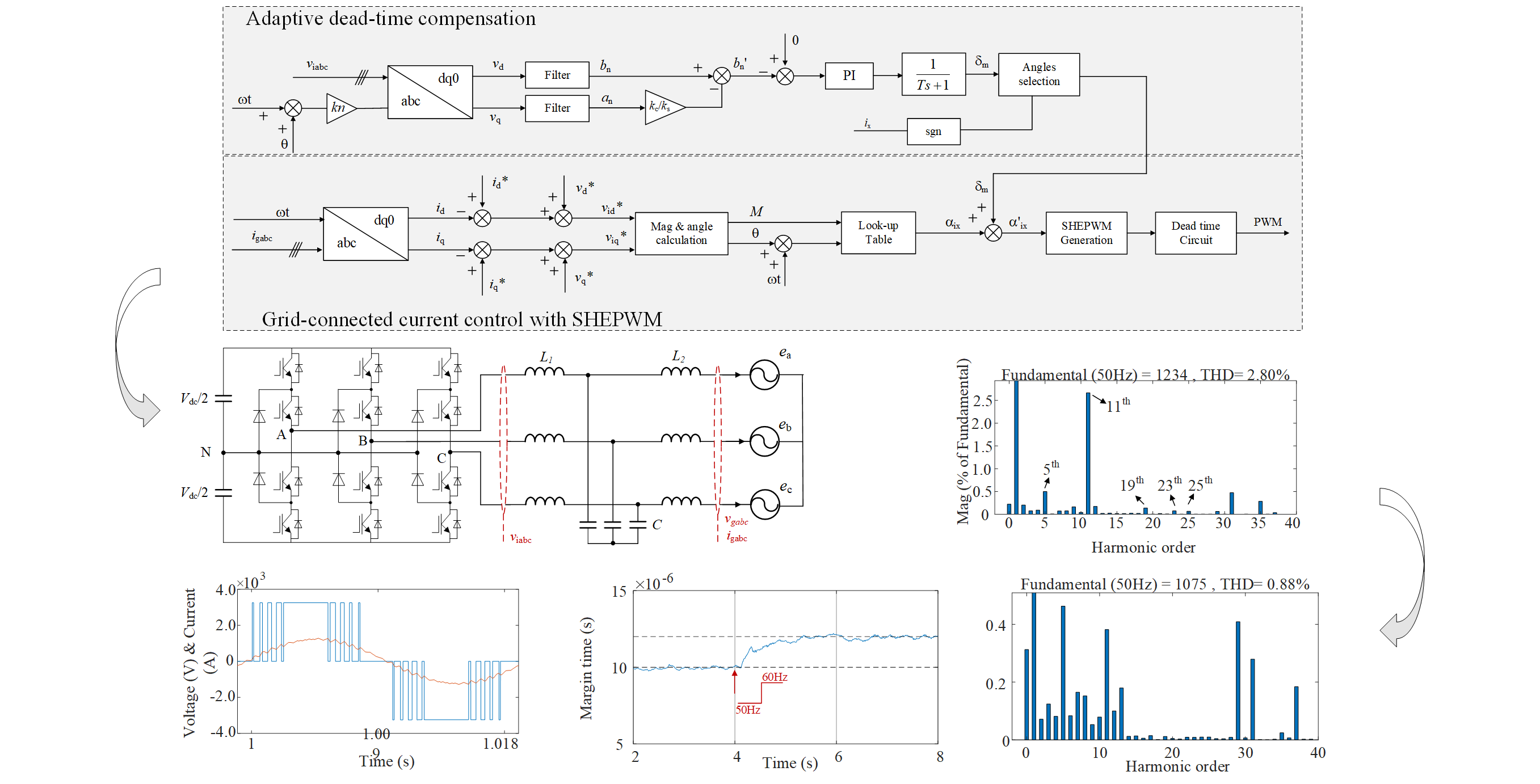
2. Modeling and Analysis of Dead-Time Effect on Three-Level SHE-PWM Modulation

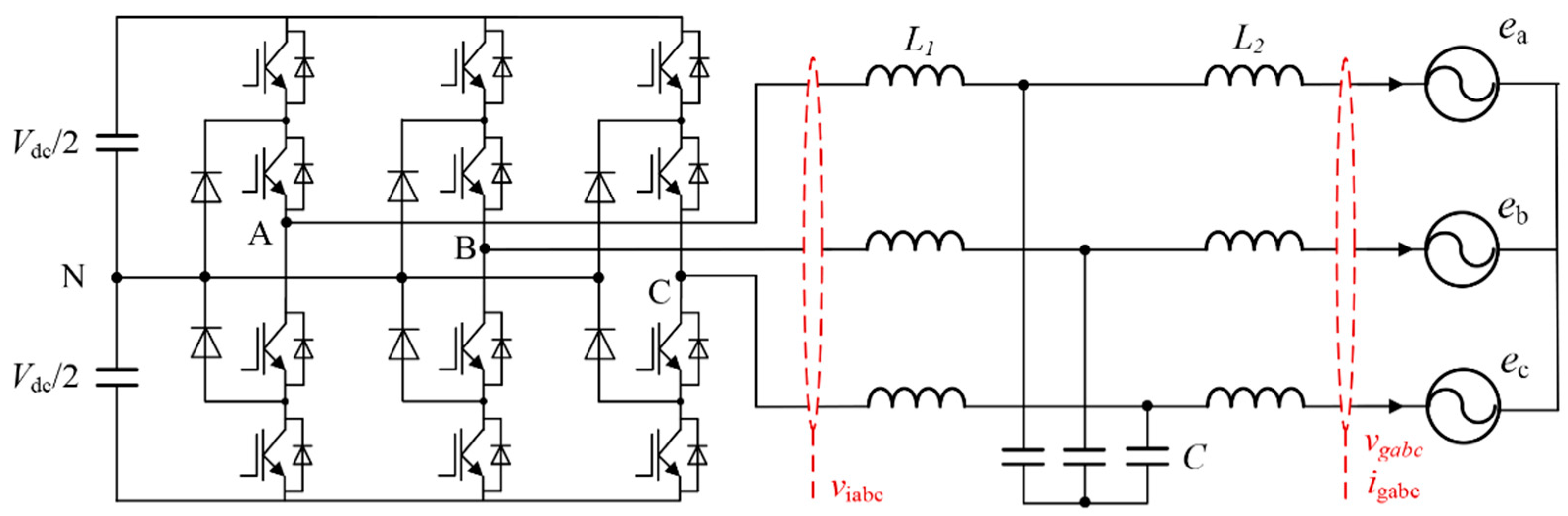
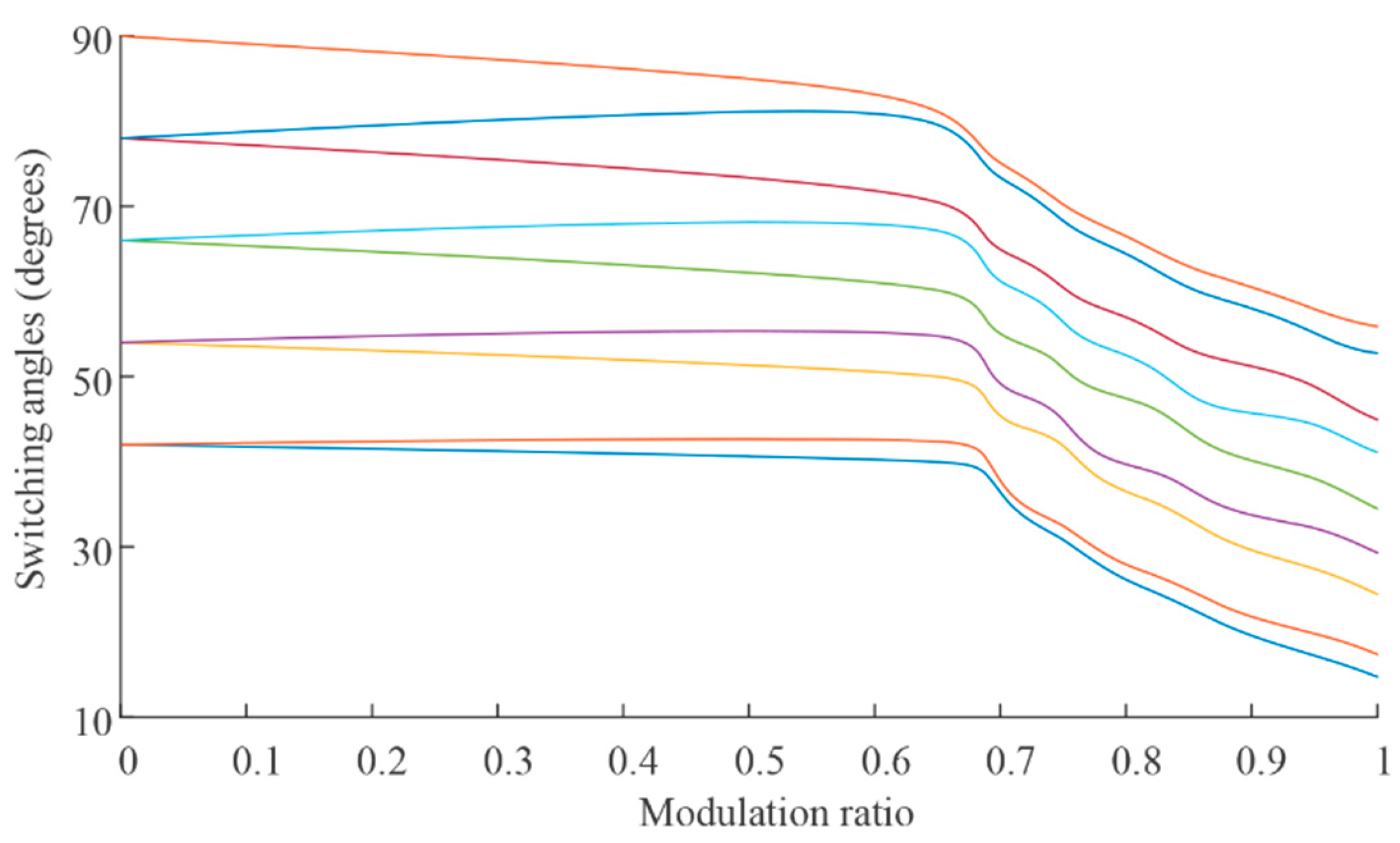
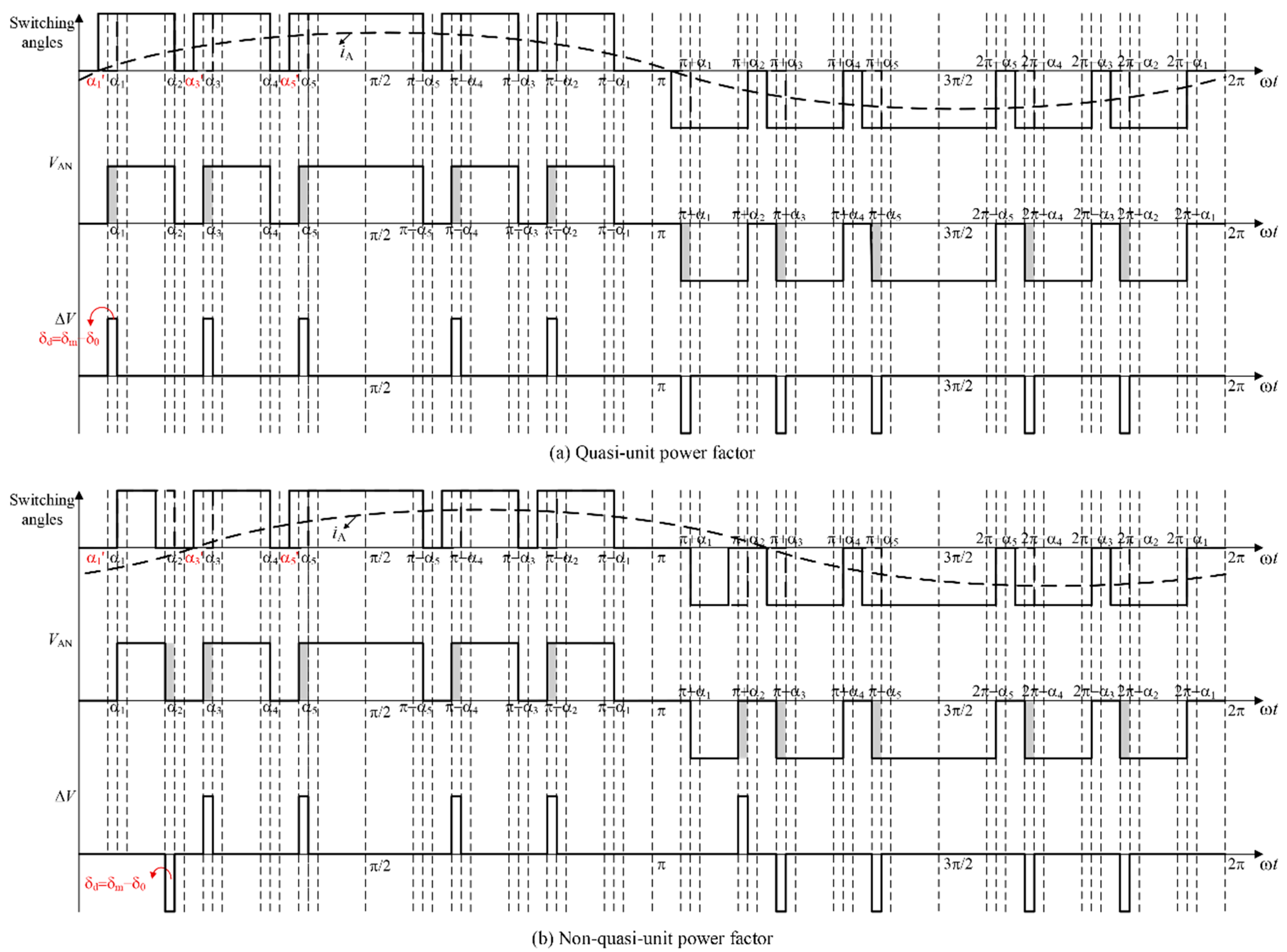
2.1. Modulation Principles of the Ideal Three-Level SHE-PWM

SHE-PWM is based on Fourier decomposition of the converter output voltage waveform, as shown by v x N (x = A, B, C) in Figure 1. By artificially arranging the number and position of the switching angles, the lower harmonics of interest in the output voltage waveform can be eliminated, thereby avoiding the appearance of the corresponding harmonics in the grid line current. The most commonly used 3-level SHE-PWM waveform shown in Figure 2 has an even quarter-wave symmetry and odd half-wave symmetry. Noted that there are researches on loosening the symmetry of the SHE-PWM waveform for the reason of extending the available solutions or controllability of harmonics, at the expense of increased computational and control strategy complexity [6]. A quarter-wave symmetry SHE-PWM is employed in this paper.
The Fourier decomposition of the quarter-wave symmetry SHE-PWM in Figure 2 is as shown in (1) and (2), in which ω ,   V dc ,   n ,   N denote the fundamental angular frequency, DC side voltage of the inverter, harmonic order and the number of switching angles over the quarter-period of the waveform, respectively.
v A N = a 0 2 + n = 1 ( a n cos ( n ω t ) + b n sin ( n ω t ) )
where
{ a n = 0 b n = 4 n π V d c 2 i = 1 N ( 1 ) i 1 cos ( n α i ) if   n   is   odd . b n = 0 if   n   is   even .
Equation (2) shows that the DC component, the harmonics of cosine terms and the even harmonics of sine terms are eliminated due to quarter-wave symmetry. Therefore, the desired fundamental voltage can be obtained and several harmonics of interest can be eliminated by selecting a set of switching angles ( α 1 α N ) that satisfy (3) (5). v 1 m and represent the expected fundamental amplitude and the set of harmonics to be eliminated, respectively. For SHE-PWM with N switching angles, apart from the regulated fundamental component a total of N 1 harmonics can be eliminated. In three phase three-line grid-connected applications, the harmonics in (5) are usually eliminated since the triple harmonics are considered as zero-sequence components which have no current path and are thereby left uncontrolled. It is clear that the bigger the N is, the smaller the harmonic distortion of the line current is, and the higher the switching loss is. A compromise is always made. When it comes to the motor drive application, the current distortion is not of primary concern. However, the low order harmonics that cause torque ripple are to be eliminated.
{ i = 1 N ( 1 ) i 1 cos ( α i ) = π 4 M i = 1 N ( 1 ) i 1 cos ( n α i ) = 0
where
{ M = 2 v 1 m / V d c n
and
= { 5 , 7 , 11 , 13 , , 3 N 2 }
Equation (3) is a set of non-linear and transcendental equations. Finding the analytical solution is of great challenge. Iterative numerical techniques such as Newton–Raphson are most commonly adopted [13,14]. Due to the problem of convergence, the equations are solved off-line over the whole modulation ratio range with a certain step size. The resulting switching angle data at different modulation ratios are stored as a table in the controller memory. Then, the real-time PWM signals are obtained by looking up the table. Generally, a real-time phase angle of the modulation voltage and the off-line solved switching angle data requires special design in a digital controller to ensure a certain accuracy [17]. Typical switching angle trajectories (e.g., N = 9 ) are shown in Figure 3.

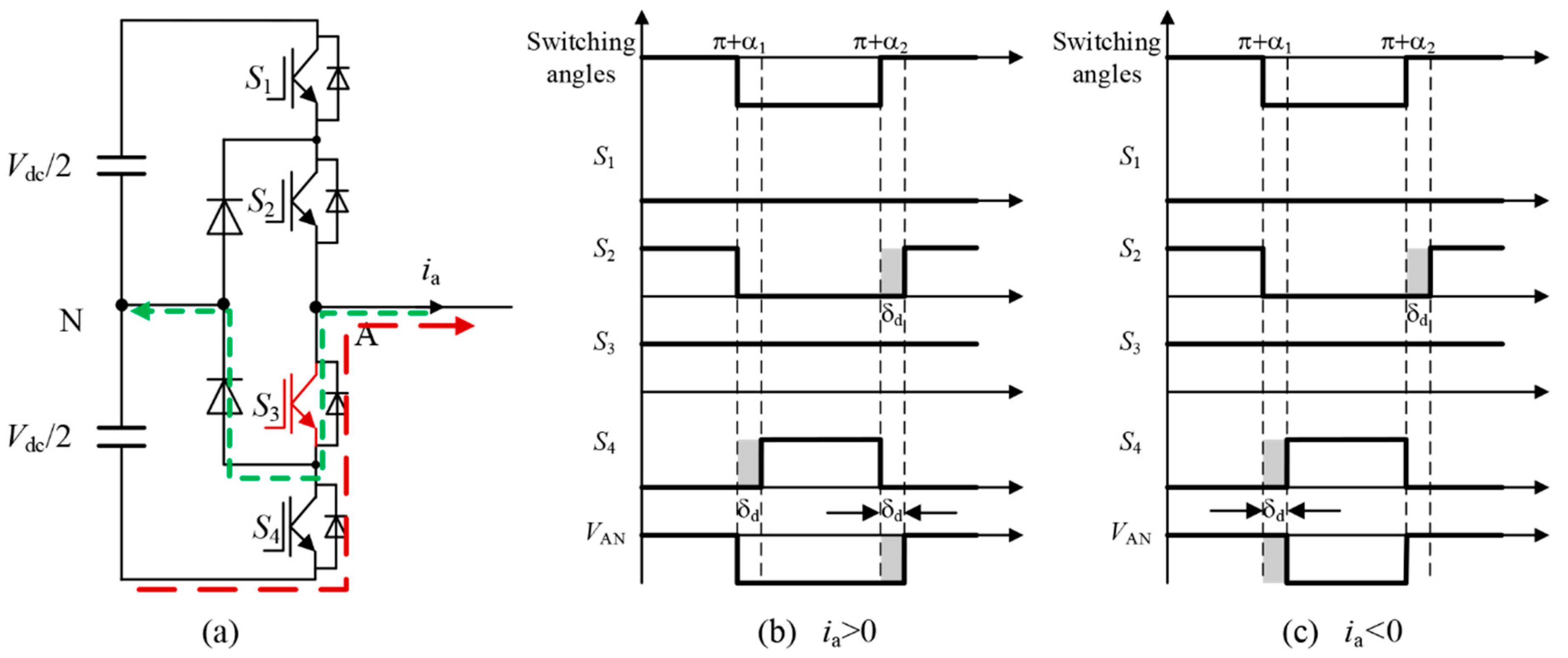
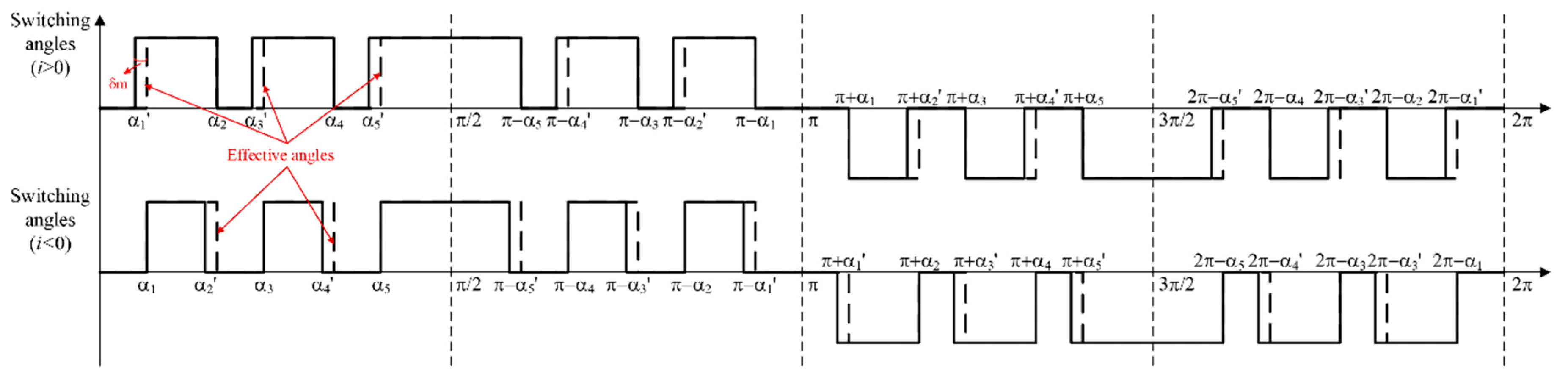
2.2. Circuit State Analysis during Dead Time

The actual switching process needs to last for a certain amount of time instead of occurring instantaneously. A dead time should be added to the driving signals of the alternating switches to avoid a bridge arm straight through [22]. The duration of dead time should be set to an appropriate value with an adequate margin. The following factors need to be considered: the rise/fall time and the turn on/off delay time of the semiconductors, the tail current of the semiconductors, the reverse recovery time of the antiparallel diodes, the drive capability, and the delay time of the hardware circuits [23]. In a system employing high power IGBTs/IGCTs, the turn on/off time is much longer than the small power semiconductors, such as MOSFETs. Furthermore, to avoid high voltage rise/fall rate (dv/dt) and switch-off over-voltage, the IGBT/IGCT drive capability is limited. These reasons make it necessary to set a dead time of up to tens of microseconds in high power IGBT/IGCT applications. The accompanying dead-time effect would reduce the harmonic performance of SHE-PWM modulation and needs to be compensated for. In the following analysis a dead time T d generated by a delay circuit in Figure 4 is adopted.
A bridge arm of the three-level NPC converter outputs three voltage levels, i.e., V d c / 2 , 0, V d c / 2 , denoted as 1, 0, −1. Under an ideal SHE modulation, the bridge arm outputs exactly the same PWM waveform as in Figure 2 by comparing the real-time phase angle of the modulation voltage with the switching angles, and achieves the desired output harmonic performance. However, performance is degraded due to the addition of the dead time and the non-ideal characteristics of the semiconductor devices. The detailed current path and output voltage during the dead time is shown in Figure 5 and Figure 6. Compared with the ideal SHE-PWM waveform, the output voltage square wave is widened or narrowed according to the current polarity, and the phase angle of the modulation voltage.
Specifically, in the positive half cycle of the modulation voltage, as shown in Figure 5a, only switch S 2 is turned on during the dead time and the current is forced through the clamped diode or the freewheeling diode. The red dashed-line and green half-dashed-line correspond to the positive current path and negative current path, respectively. As a consequence, during the dead time the bridge arm outputs level 0 at positive current polarity as in Figure 5b, and level 1 at negative current polarity as in Figure 5c. The shadowed parts denote the output voltage error compared with the ideal SHE-PWM waveform. Noted that δ d (in radians) is the equivalent dead time considering the deliberately introduced dead time T d and the non-ideal characteristics of the semiconductors. Figure 6 illustrates the situation in the negative half cycle of the modulation voltage. The similar analysis is omitted.

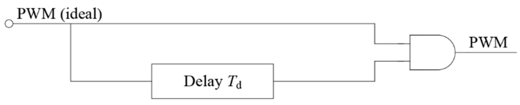
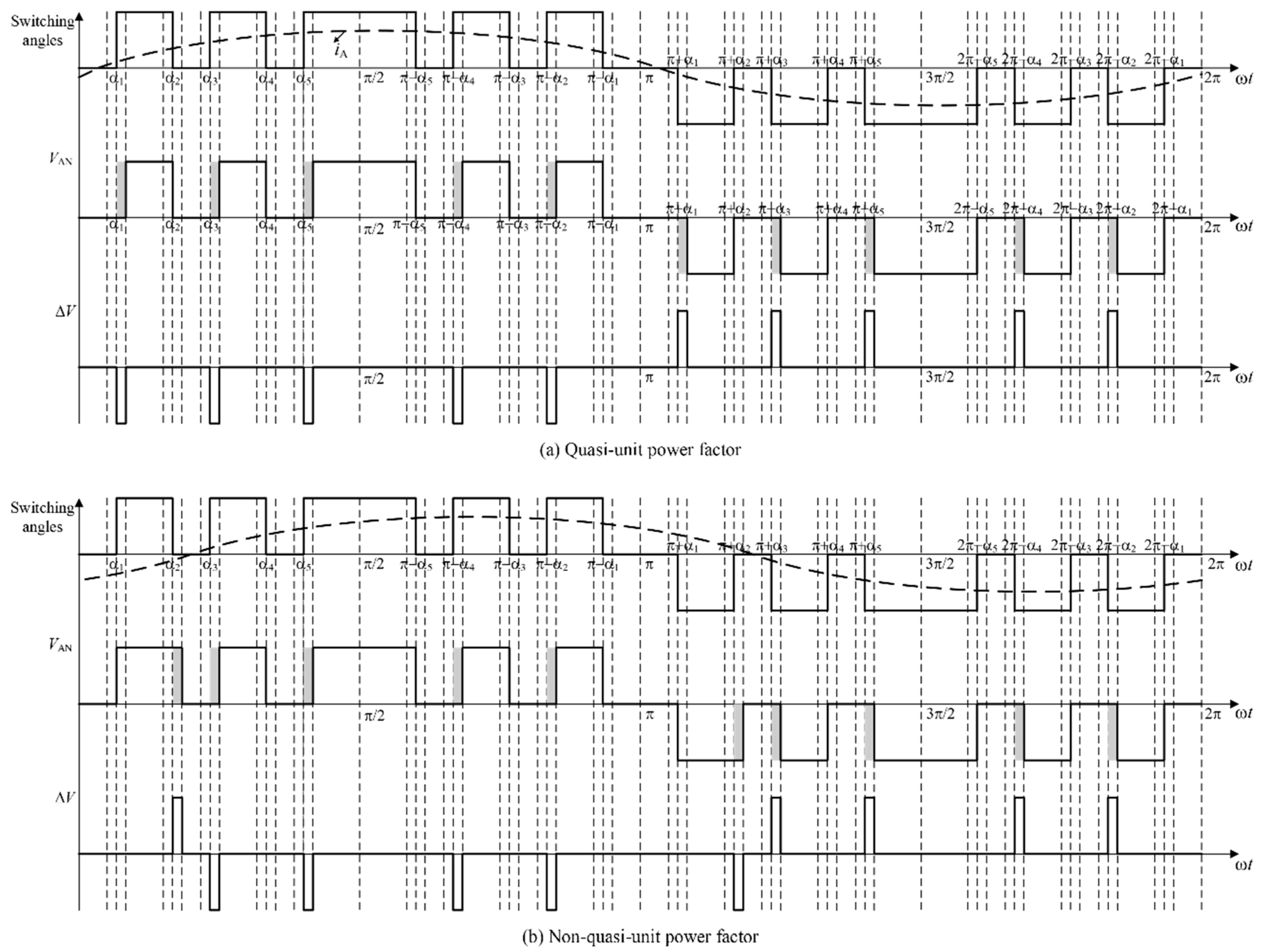
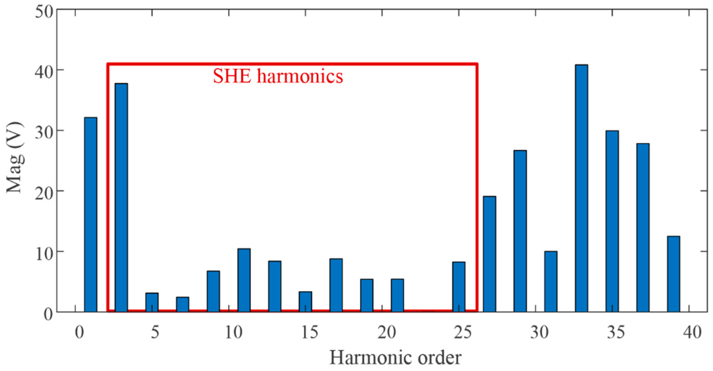
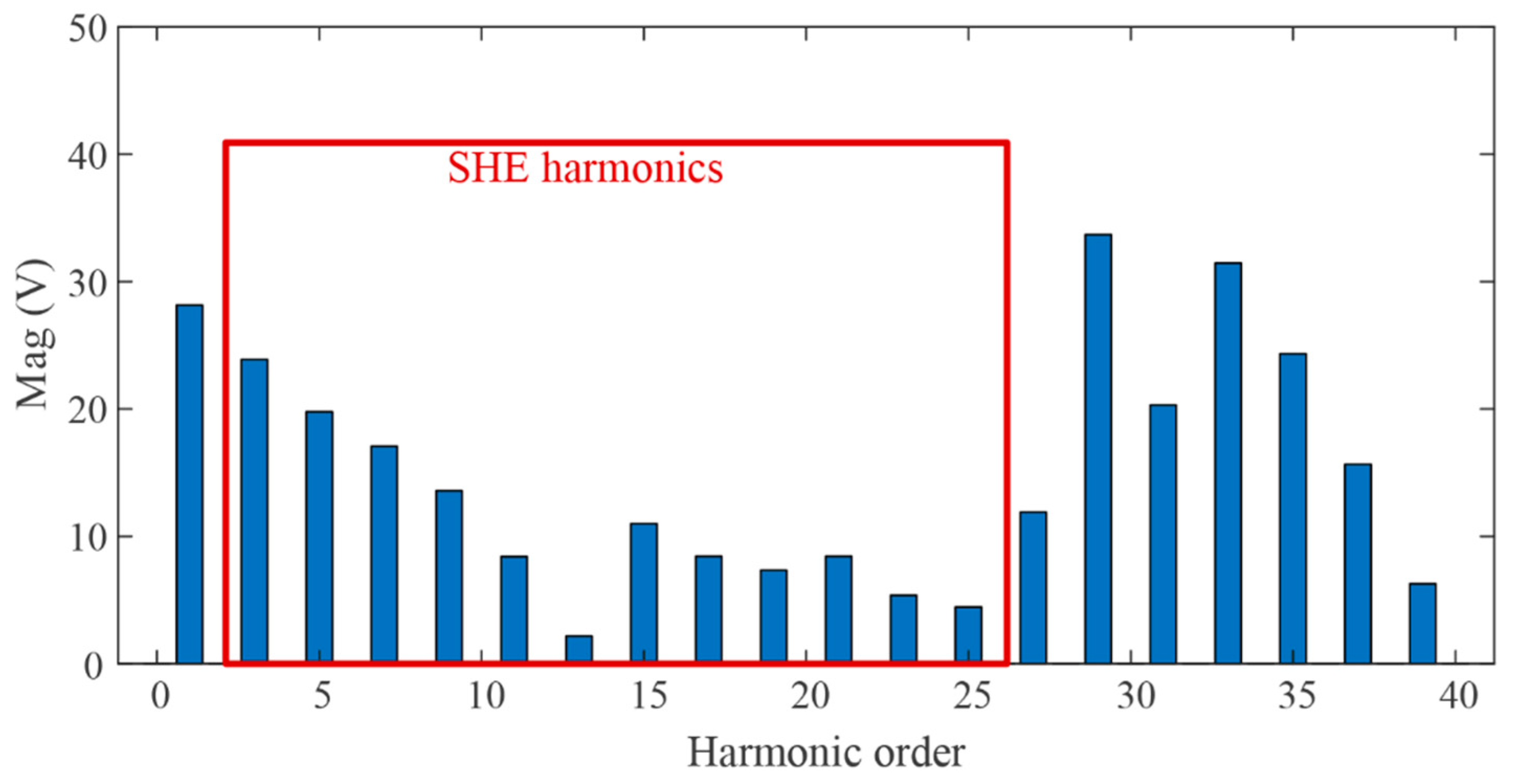
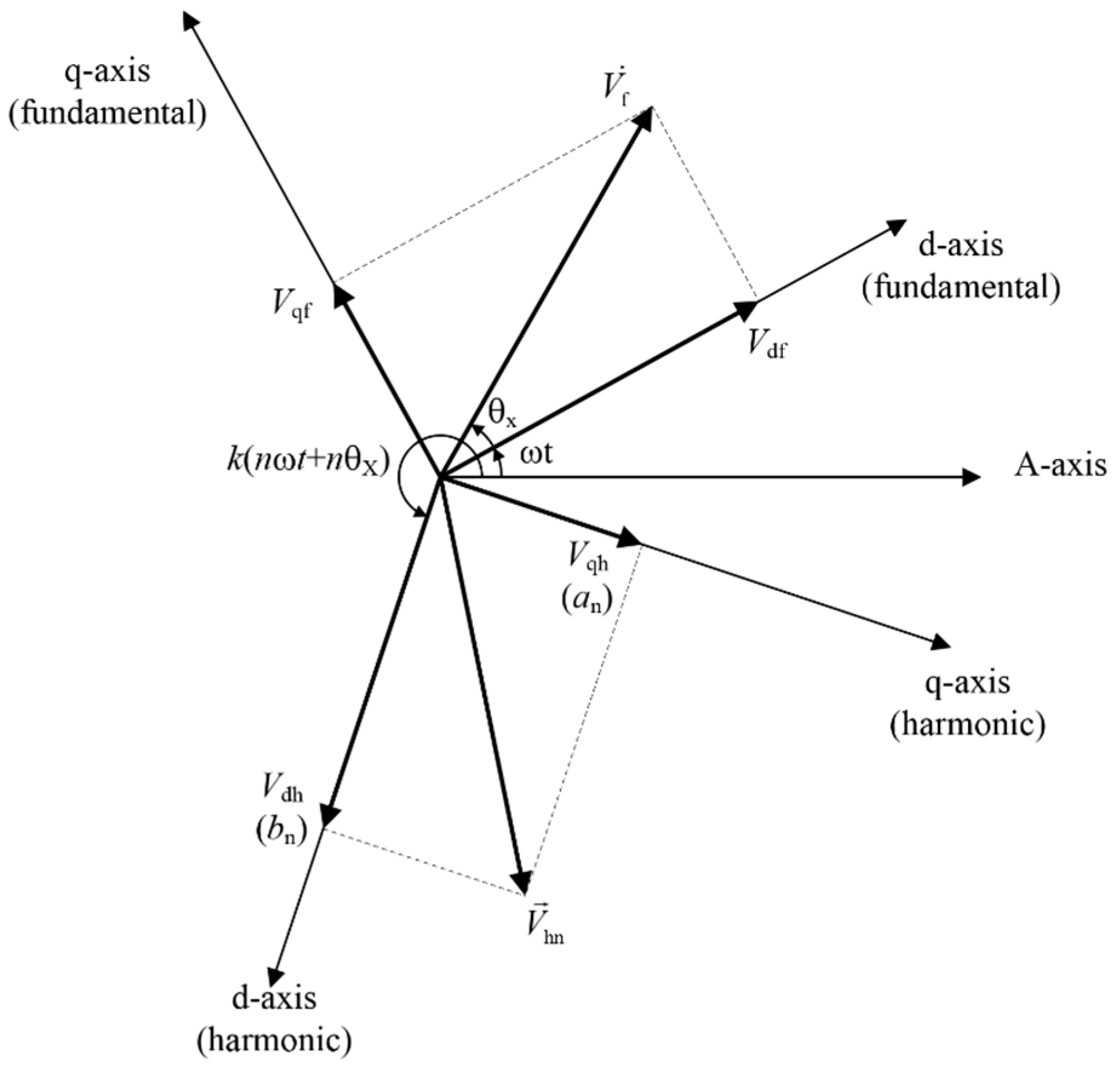
2.3. Modeling of Dead-Time Effect

In general, the introduction of the dead time has changed the specific switching instant, which makes equation 3 no longer hold. This will affect the precise control of the fundamental component and lead to the generation of harmonics. A simpler case is considered first where the power factor angle θ is between α 1 and α 1 . This is hereinafter referred to as the quasi-unit power factor as shown in Figure 7a. The error between the output voltage and the ideal SHE-PWM remains negative when ω t is between 0 and π, and positive when ω t is between π and 2π.
The output voltage waveform is the superposition of the ideal SHE-PWM waveform and the error voltage waveform. By performing Fourier decomposition on the error voltage waveform, Δ V , the result in (6) can be obtained (on page 7). It is seen that odd low-order harmonics including the fundamental component are introduced. The harmonic distribution calculated from (6) using the switching angle data in Figure 3 ( N = 9 ) is shown in Figure 8. The triple harmonics are still considered as zero-sequence in a three phase symmetrical system though, others, for example, 5th, 7th, and 11th harmonics will introduce corresponding current harmonics which is undesired in grid-connected applications. Equation (6) is a general expression for harmonics of Δ V in the full frequency range. However, the low-order harmonic parts contained in the set are of primary concern. Those harmonics referred to as SHE harmonics Δ V S H E have a more simplified expression by substituting (3) (4) into (6) as in (7).
{ Δ V = a 0 2 + n = 1 ( a n cos ( n ω t ) + b n sin ( n ω t ) ) a 0 = 0 a n = { 2 n π ( i = 1 N sin ( n α i ) cos ( n δ d ) 1 ) + i = 1 N ( 1 ) i 1 cos ( n α i ) ( 1 sin ( n δ d ) ) n   is   odd . 0 n   is   even . b n = { 2 n π ( i = 1 N sin ( n α i ) sin ( n δ d ) + i = 1 N ( 1 ) i 1 cos ( n α i ) ( 1 cos ( n δ d ) ) ) n   is   odd . 0 n   is   even .
{ Δ V S H E = n ( a n cos ( n ω t ) + b n sin ( n ω t ) ) a n = 2 n π i = 1 N sin ( n α i ) ( cos ( n δ d ) 1 ) b n = 2 n π i = 1 N sin ( n α i ) sin ( n δ d )
Next, the complicated case where the power factor angle θ is beyond α 1 α 1 is addressed. As shown in Figure 7b, the error voltage now is more “irregular”, since the current polarity has changed once along the switching angles. Assuming a general case that the current zero-crossing occurs between α x and α x + 1 , then the Fourier decomposition of the error voltage in this case is shown in (8). similarly, by substituting (3) (4) into (8), a simplified expression of Δ V S H E is obtained as in (9). Obviously, (9) is more complicated than the case in (7), since it is a polynomial combination of different trigonometric functions of dead time. This brings considerable trouble in the subsequent dead-time compensation strategy. The harmonic distribution calculated by (8) is shown in Figure 9. The harmonic distribution differs from that in Figure 8 and the low order harmonics such as the fifth and seventh are larger. Noted that (9) will be degraded to (7) if x is set to zero.
{ Δ V = a 0 2 + n = 1 ( a n cos ( n ω t ) + b n sin ( n ω t ) ) a 0 = 0 a n = { 2 n π ( i = 1 N cos ( n α i ) sin ( n δ d ) + i = x + 1 N sin ( n α i ) ( cos ( n δ d ) 1 ) + i = 1 x ( 1 ) i 1 cos ( n α i ) sin ( n δ d ) n   is   odd . 0 n   is   even . b n = { 2 n π ( i = 1 N cos ( n α i ) cos ( n δ d ) 1 ) + i = x + 1 N sin ( n α i ) ( sin ( n δ d ) i = 1 N ( 1 ) i 1 cos ( n α i ) cos ( n δ d ) n   is   odd . 0 n   is   even .
{ Δ V S H E = n ( a n cos ( n ω t ) + b n sin ( n ω t ) ) a n = 2 n π ( i = 1 x cos ( n α i ) sin ( n δ d ) + i = x + 1 N sin ( n α i ) ( cos ( n δ d ) 1 ) ) b n = 2 n π ( x = 1 x cos ( n α i ) ( cos ( n δ d ) 1 ) + i = x + 1 N sin ( n α i ) sin ( n δ d ) )
.

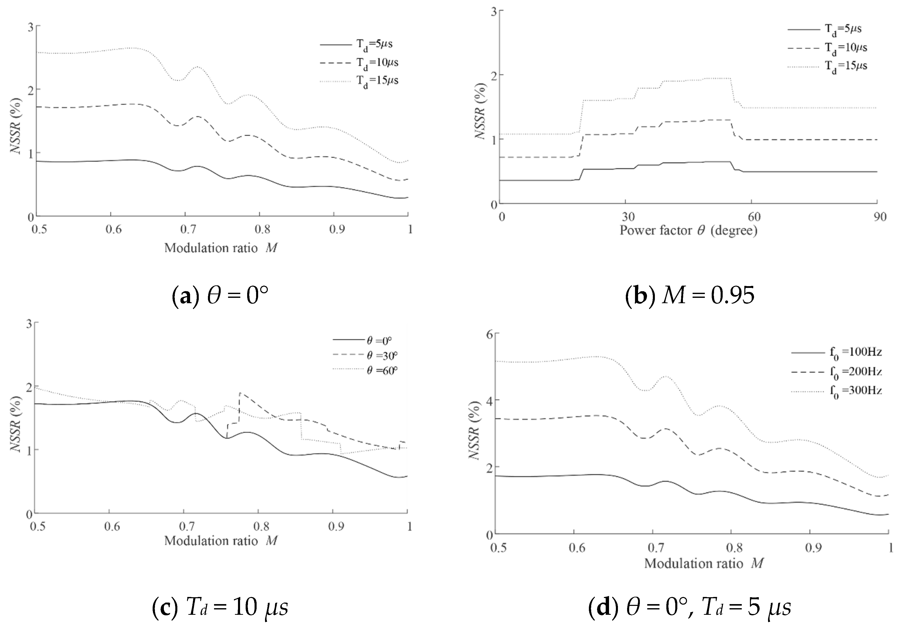
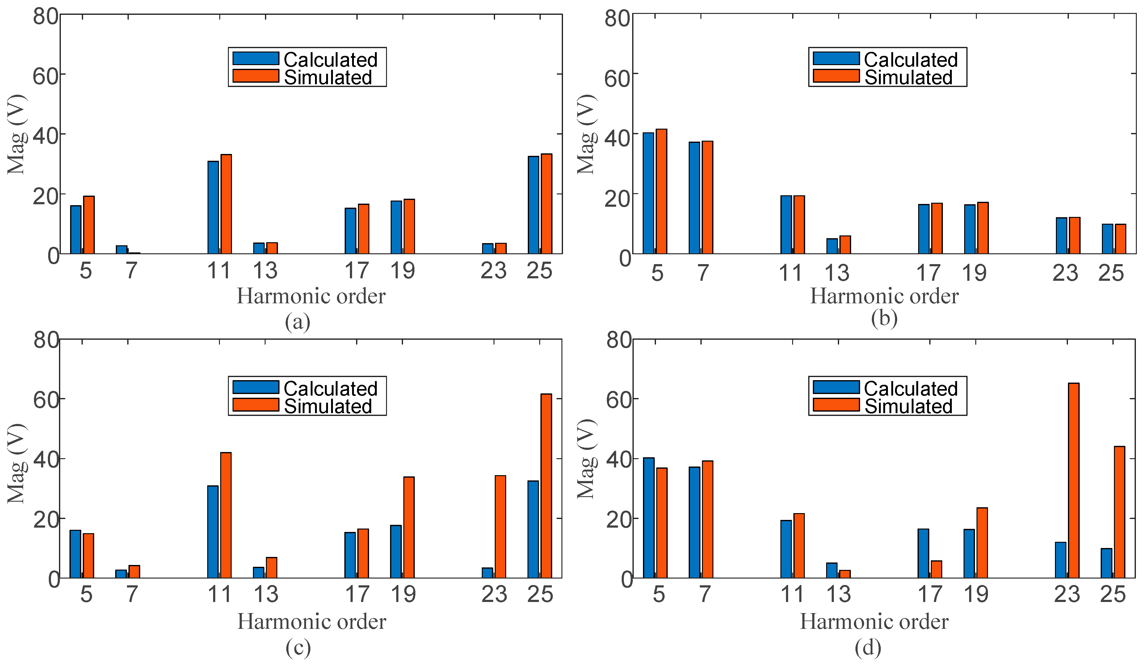
2.4. Dead-Time Effect under Different Operation Conditions

This section compares the dead-time effects under different operation conditions including the size of dead time δ d ( δ d = T d × 2 π f 0 ), modulation ratio M , and power factor angle θ . It can be seen that the effect of the change in fundamental frequency f 0 is the same as the change of the dead time δ d , because SHE-PWM is naturally a synchronous modulation technique [32]. The normalized square sum root (NSSR) of the amplitude of the SHE harmonics (harmonics in the set ) shown in (10) is used to evaluate the dead-time effect. It should be noted that the NSSR directly reflects the harmonic voltage generated by the dead-time effect. However, it should not be considered equivalently as the total harmonic distortion (THD) of the gird current which is much worse because of the impact of the uneliminated harmonics, grid voltage harmonics, resonance peak of the LCL filter, etc.
N S S R   =   n a n 2 + b n 2 v 1 m 2   =   n a n 2 + b n 2 M 2 ( V d c / 2 ) 2  
The NSSR is calculated utilizing the formulation in (9), (10) and the switching angle data in Figure 3. The results obtained at different sizes of dead time, modulation ratio and power factor angle are shown in Figure 10a–d. It can be concluded that:
  • The longer the dead time, the severer the dead-time effect, at any power factor angle or modulation ratio, as shown in Figure 10a,b.
  • Dead-time effect is nonlinearly distributed over the entire modulation ratio range, but decreases overall as the modulation ratio increases as shown in Figure 10a,c.
  • The power factor angle θ has a large impact on dead-time effect. And the dead-time effect is basically lighter at quasi-unit power factor, as shown in Figure 10b,c.
  • The dead-time effect remains the same when the power factor angle varies between two adjacent angles, as shown in Figure 10b.
  • The dashed line ( θ = 30 ) remains coincident with the solid line ( θ = 0 ) in Figure 10c when the modulation ratio is less than 0.76. This is because the quasi-unit power factor range is greater than 30 when the modulation ratio is small as shown in Figure 3.
A special case where the fundamental frequency changes in a motor drive application is illustrated in Figure 10d. It is shown that the dead-time effect is the same with that in Figure 10a but becomes much severer in high frequency applications.

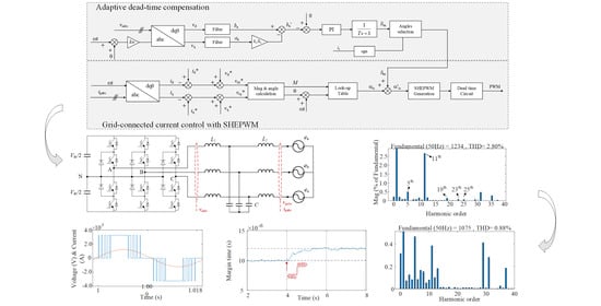
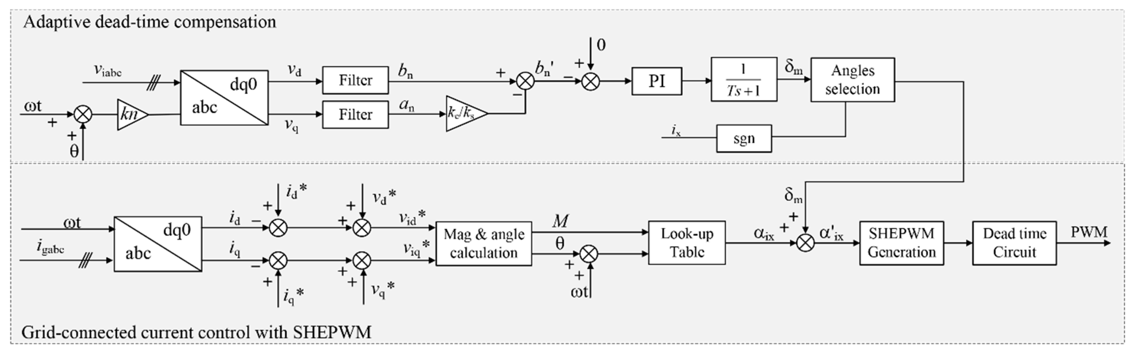
3. Dead-Time Compensation Method

Quarter-wave symmetry SHE-PWM is considered a “pure-sinusoidal” modulation technique which doesn’t have any control abilities on the harmonic components. As a consequence, the feedback or feedforward dead-time compensation strategy on SPWM/SVPWM in the available literature cannot be applied to SHE-PWM [21,28]. On the other hand, the prestored switching angles in the digital controller make it easy to modify the pulse width and thus to compensate for the dead-time effect. Based on above analysis, this chapter proposes an open-loop dead-time compensation method by inserting a margin time into the effective switching angles. Furthermore, the online adaptive adjustment of the margin time is realized by a closed-loop feedback control of a specific harmonic voltage component. The closed-loop compensation method will facilitate the performance of SHE-PWM in a variable frequency application.

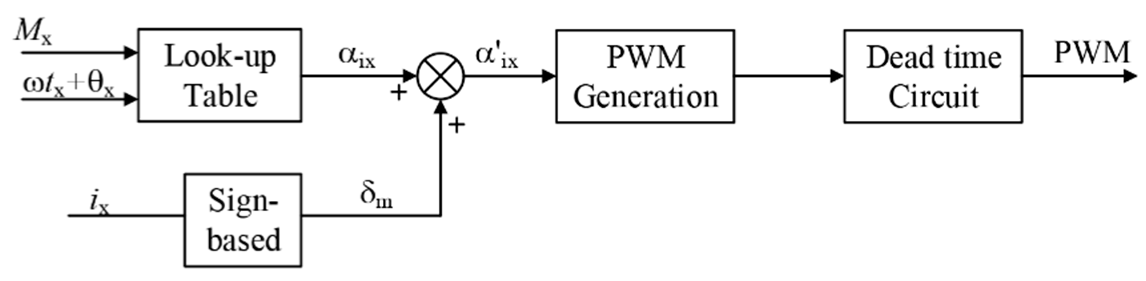
3.1. Open-Loop Dead-Time Compensation Method

From Figure 5 and Figure 6, it can be learned that the PWM pulse is narrowed or widened according to the current polarity. Specifically, the high-level pulse width is narrowed on the left side when the current is positive, and widened on the right when the current is negative. Noted that one in the positive half cycle and zero in the negative half cycle of the PWM are regarded as high-level. These affected switching angles are regarded as effective angles in the following section. Hence, the dead-time compensation can be easily achieved by inserting a margin time δ m into the effective switching angles before the PWM generation to counteract the dead-time effect as shown in Figure 11. This is easy to implement because the switching angle data are calculated off-line and stored in the controller already. Judging the polarity of the current might be a trouble, though there are lots of studies available for reference [20,23,27]. Generally, the switching angles in the first quarter are obtained by looking up the table, while the ones in other quarters are obtained by symmetry. To avoid confusion, Table 1 gives the insertion rules of the margin time. And Figure 12 illustrates the implementation of the margin time insertion.
The compensated switching angles are no longer quarter-wave symmetrical as shown in Figure 12. However, referring to the analysis in Figure 5 and Figure 6, the output PWM will restore quarter-wave symmetry and be close to the ideal SHE-PWM waveform after considering the dead time. A full compensation is achieved if the margin time δ m equals the dead time δ d . It is worth highlighting that the above method has limited performance in practical applications, since it is an open-loop compensation method. In practice, apart from the deliberately inserted dead time, there are other uncertain factors contributing to the dead-time effect, such as the rise and fall time and the turn on/off delay time of the semiconductors, the drive capability, the reverse recovery time in antiparallel diodes, and other disturbance. Worse cases occur when SHE-PWM is involved in a variable frequency application. A closed-loop compensation method is more acceptable and reliable

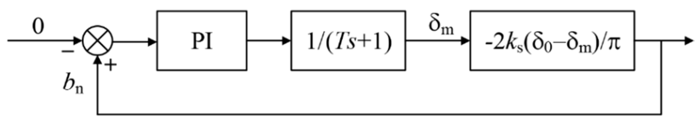
3.2. Closed-Loop Dead-Time Compensation Method

Still, the simpler case of the quasi-unit power factor is discussed first. Recall that the coefficient b n of the sine term in (7) is as follows:
b n = 2 n π i = 1 N sin ( n α i ) sin ( n δ d )
The dead time δ d is quite small, then
{ b n 2 δ d π i = 1 N sin ( n α i ) = 2 π k s δ d k s = i = 1 N sin ( n α i )
In (12), parameter k s is a function of the switching angles, or specifically, a function of the modulation ratio M which is the look-up table index for the prestored angles. In a grid-connected application, the modulation ratio remains the same or only changes slowly. Therefore, the coefficient b n is considered as a linear function of the dead time δ d . Based on this, this paper proposes an adaptive dead-time compensation method, where a margin time δ m is calculated online through a closed-loop feedback controller to compensate for the dead time δ 0 as shown in Figure 13. The sine-term component of a certain harmonic voltage is fed back and a simple proportional integral (PI) controller is adopted. The control loop guarantees a zero static error because of the linearity of the model. A first-order inertia is added to increase the stability of the system. Noted that δ 0 and δ m in Figure 13 represent the equivalent dead time and the margin time, respectively.
The question which remains here is how to extract the sine-term of the certain harmonic voltage amplitude, i.e., b n . Recall that in Figure 7, the output voltage V x N is the superposition of the ideal SHE-PWM and the dead-time error voltage Δ V . In the SHE frequency range (SHE harmonics in set ), the Fourier decomposition of V x N is shown in (13). Parameters a n and b n are the same as in (7). Shift the x-axis to get a more generic expression as in (14), where θ x denotes the phase angle of phase x ( x = A , B , C ) modulation voltage. Therefore, the extraction of b n can be implemented in a synchronous d-q frame where the rotating phase angle can be extracted directly from the main control loop. By aligning the d-axis of the d-q synchronous frame to k ( n ω t + n θ x ) as shown in Figure 14, the amplitude of the sine-term component of the certain harmonic can be extracted out since it appears as a DC component of the d-axis. An average value filter and a low-pass filter is suggested. The parameter k should be set to 1 or 1 , respectively, when the selected harmonic component is of positive sequence or negative sequence. So far, the closed-loop compensation method shown in Figure 13 is realized for the quasi-unit power situation.
V x N = M V d c 2 sin ω t + n ( a n cos ( n ω t ) + b n sin ( n ω t ) )
V x N = M V d c 2 sin ( ω t + θ x ) + n ( a n cos ( n ω t + n θ x ) + b n sin ( n ω t + n θ x ) )
Again, the more complex situation is discussed where the power factor angle is beyond α 1 α 1 . As shown in (9), the magnitude of the sine-term b n of the harmonic voltage is no longer linearly related to the dead time δ d . Simply applying the above control strategy in Figure 13 will lead to instability. Rewrite (9) into (15) and (16). It can be seen that the nonlinearity of b n can be corrected by “cross decoupling” with a n , as shown in (17). It should be noted that (17) will be degraded to (12) when x = 0 . Now that as long as using b n instead of b n as the feedback variable, the control strategy in Figure 13 will apply to any power factor angle.
{ Δ V S H E = n ( a n cos ( n ω t ) + b n sin ( n ω t ) ) a n = 2 n π ( k c sin ( n δ d ) + k s ( cos ( n δ d ) 1 ) ) b n = 2 n π ( k c ( cos ( n δ d ) 1 ) + k s sin ( n δ d ) )
where
{ k c = i = 1 x cos ( n α i ) k s = i = x + 1 N sin ( n α i )
b n = b n k c k s a n = 2 ( k s 2 + k c 2 ) n π k s sin ( n δ d ) 2 π ( k s + k c / k s ) δ d
The complete control strategy for adaptive dead-time compensation is shown in Figure 15. The control strategy consists of two parts, i.e., the grid-connect current control strategy and the adaptive dead-time compensation strategy. The dead-time compensation strategy is implemented in a synchronous d-q frame at a certain harmonic frequency. The parameters ω t and θ required for the orientation of the d-axis can be obtained from the current control loop. This is easy to implement because the current control loop in the grid-connected application is usually carried out in a synchronous d-q frame at the fundamental frequency.

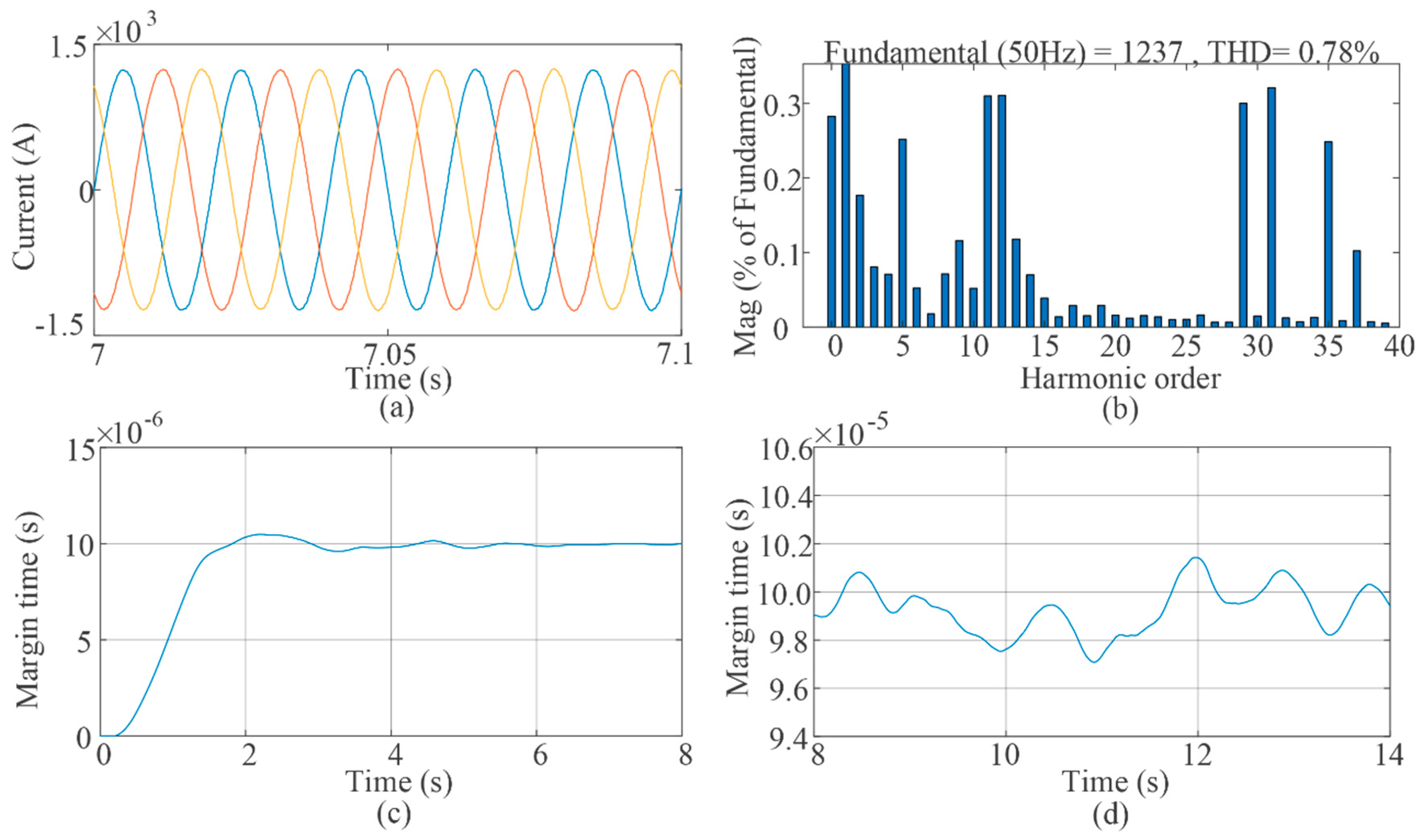
3.3. Convergence Analysis on Closed-Loop Control

The dynamic of the above control loop of the quasi-unit power factor angle is discussed as follows. During the dynamic process, there is an error between the compensation angle δ m and the equivalent dead time δ 0 . When δ m < δ 0 , an under-compensation happens, and the error voltage waveform is similar to Figure 7a. By substituting δ d = δ 0 δ m into (7), the SHE harmonic distribution of the error voltage waveform when under-compensation happens can be obtained as in (18).
{ Δ V S H E = n ( a n cos ( n ω t ) + b n sin ( n ω t ) ) a n = 2 n π i = 1 N sin ( n α i ) ( cos ( n ( δ 0 δ m ) ) 1 ) b n = 2 n π i = 1 N sin ( n α i ) sin ( n ( δ 0 δ m ) )
When δ m > δ 0 , an over-compensation happens, and the error waveform at the quasi-unit power situation is shown in Figure 16a which is different from that in Figure 7a. Applying the Fourier decomposition on the waveform in Figure 16a results in (19) which differs from (6). However, the harmonic distribution in the SHE frequency range can be obtained by substituting (3) into (19) results in (20). By substituting δ d = δ m δ 0 , the outcome is exactly the same with (18). This means that although over-compensation and under-compensation occur alternately during dynamic processes, the mathematical model of the dead-time effect remains unchanged and linear. The above properties ensure that the dynamic process will safely enter the steady state.
{ Δ V = a 0 2 + n = 1 ( a n cos ( n ω t ) + b n sin ( n ω t ) ) a 0 = 0 a n = { 2 n π ( i = 1 N sin ( n α i ) ( cos ( n δ d ) 1 ) i = 1 N ( 1 ) i 1 cos ( n α i ) sin ( n δ d ) ) if   n   is   odd . 0 if   n   is   even . b n = { 2 n π ( i = 1 N sin ( n α i ) sin ( n δ d ) + i = 1 N ( 1 ) i 1 cos ( n α i ) ( 1 cos ( n δ d ) ) ) if   n   is   odd . 0 if   n   is   even .
{ Δ V S H E = n ( a n cos ( n ω t ) + b n sin ( n ω t ) ) a n = 2 n π i = 1 N sin ( n α i ) ( cos ( n δ d ) 1 ) b n = 2 n π ( i = 1 N sin ( n α i ) sin ( n δ d ) )
At last, it is pointed out that when an over-compensation occurs with a non-quasi-unit power factor angle as shown in Figure 16b, the conclusions obtained in the case of a quasi-unit power factor angle still applies. That is, the waveform of the error voltage changes, but the mathematical model remains exactly the same in the SHE frequency range. The similar analysis is omitted.

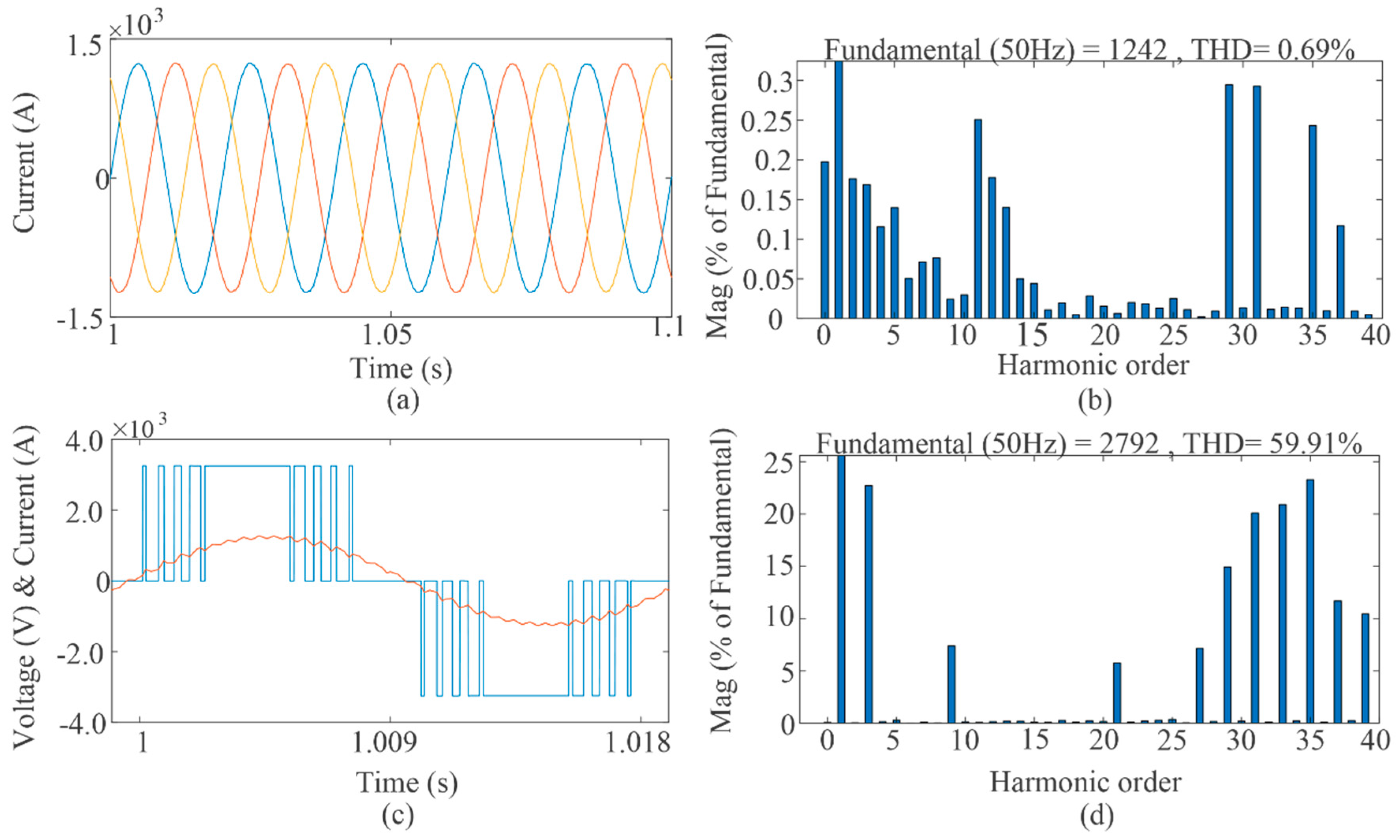
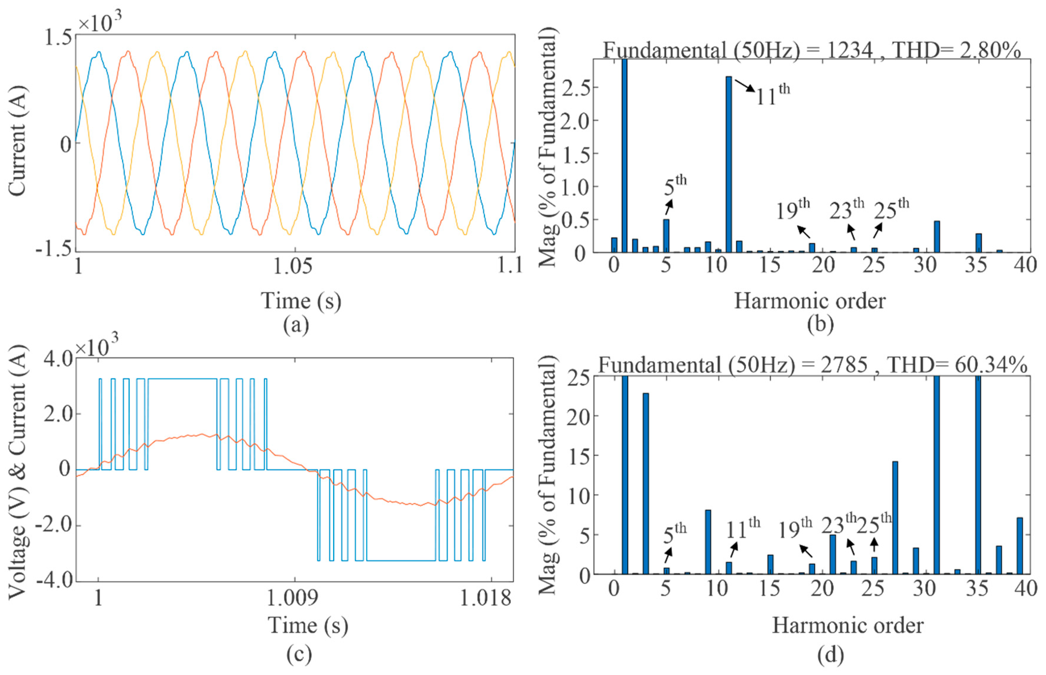
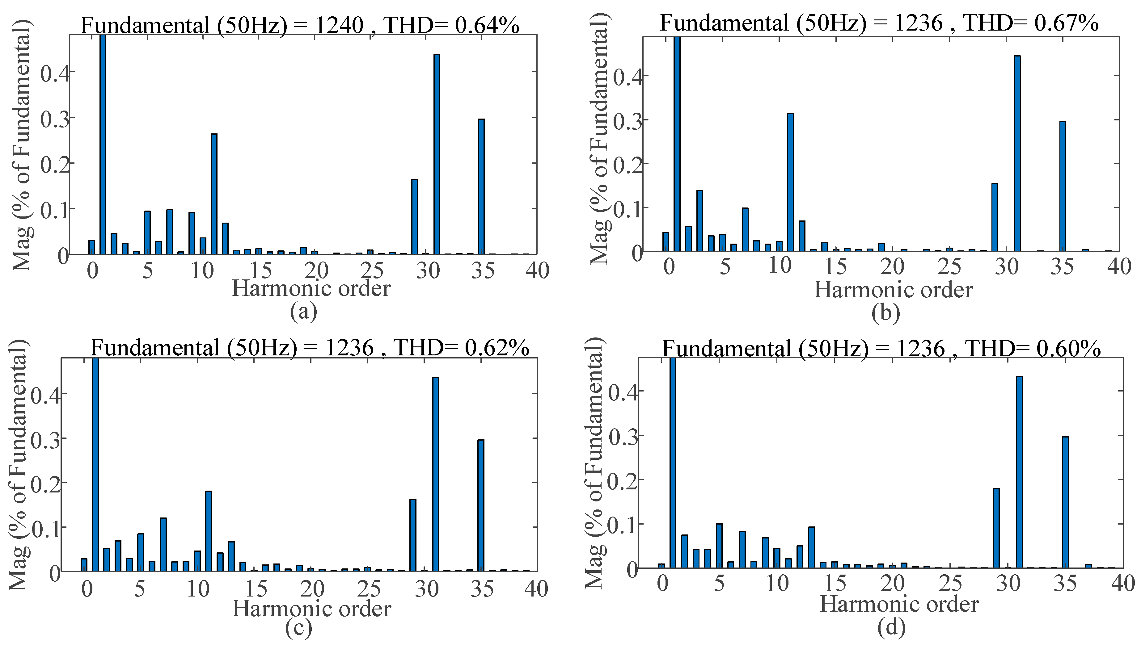
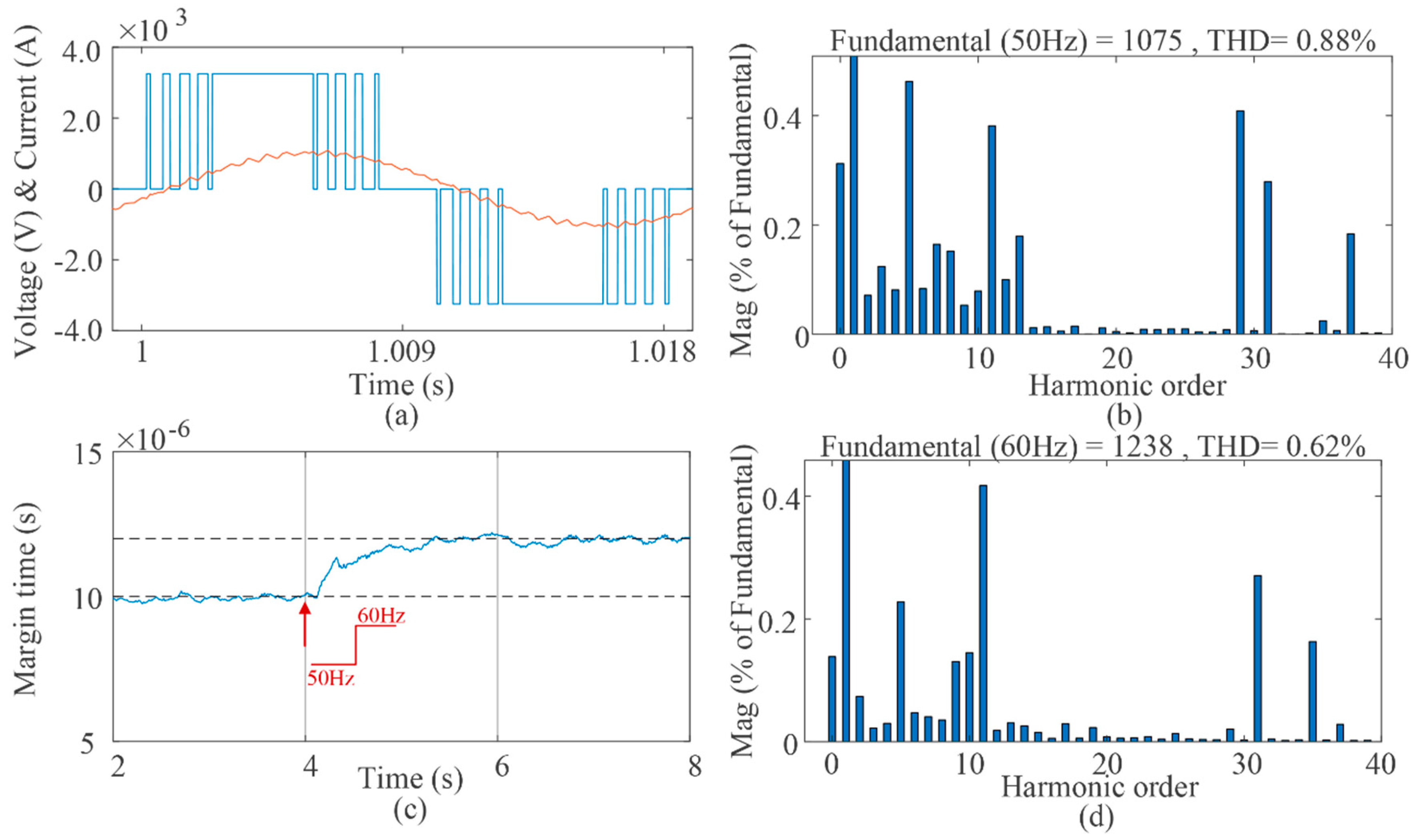
4. Simulation Results

Permanent magnet direct drive wind power generation (PMDD-WG) is a typical application of medium voltage high power grid-connected converters. 3-Level NPC converters and the SHE-PWM modulation method would be good choices to meet the stringent THD requirements of the line currents and volume requirements, especially when the system is built on an offshore platform. In order to verify the above proposed dead-time compensation method, a 3.3 kV/5 MW PMDD-WG model was built in the Simpowersystem/Simulink simulation toolbox. The topology in Figure 15 and the control strategy in Figure 15 were adopted. Simulation parameters are shown in Table 2. Comparison results of different scenarios are shown in Figure 17, Figure 18, Figure 19, Figure 20 and Figure 21. Refer to [18] for the detailed design process of the LCL filter. The main considerations are as follows:
  • The resonant frequency should be lower than half of the lowest harmonic frequency, which will provide a sufficient attenuation to filter out the harmonics. For a 9-pulse SHE modulation, the lowest harmonic frequency locates at (3N + 2) f0 = (3 × 9 + 2) × 50 = 1450 Hz. As a result, the filter resonant frequency used in the simulation was designed as 580 Hz.
  • The damping ratio needs to be set reasonably to reduce the risk of system oscillations. At the same time, the power loss of the damping resistor should be limited.
  • The reactive power capacity of the filter needs to be limited.
  • The performance and the size of the filter should be compromised.
Figure 7a–d shows the simulation results when the converter outputs 5 MW of active power which is considered the case of a quasi-unit power factor angle. An ideal SHE-PWM modulation (no dead-time effect) is employed as a comparison. It is seen that the bridge arm outputs a desired SHE-PWM waveform where the SHE harmonics are eliminated and the high-order harmonics attenuated by the output filter resulting a line currents THD value as low as 0.69%. Although there are triplen harmonic voltages which exist in the output voltage, corresponding harmonic currents are not included in the line currents. Figure 18a–d shows the simulation results under the same conditions as in Figure 17, except that a 10 μs dead time is inserted into the gate pulse. It can be seen that the line currents are significantly distorted, and the THD value increases to 2.8%. The dead-time effect leads to the occurrences of low-order harmonic voltages such as the 5th, 11th, 19th, etc. Corresponding current harmonics appear in the line currents, among which the 11th harmonic is up to 2.5%. It is because the 11th harmonic is located near the positive resonant peak of the LCL filter and is amplified. This may exceed the allowable single harmonic current injection range required by the grid-connected standards.
In Figure 19, the calculated SHE harmonic components based on model in Section 2.3 are compared with the simulated results in different operating points. Simulations are implemented with open loop (Figure 19a,b) and closed loop control (Figure 19c,d). It can be seen that the calculated values match the simulation results very well both at quasi-unit and non-quasi-unit power factors under open loop control. The correctness of the model is verified. The slight differences come from the non-ideal switching characteristics of the IGBT module including the on-state resistance, snubber resistance/capacitance, etc. Under the closed-loop control, the calculated values match the simulation results at lower frequency bands. However, the differences at the 23rd and 25th are much bigger. In this case, the steady-state error of the closed loop makes the modulation ratio (modulation ratio is the index to switching angles) different from the theoretical value, which contributes most of the differences.
After applying the proposed closed-loop dead-time compensation method, the line currents recover sinusoidally and the THD value drops to 0.78% as shown in Figure 20a–d. The harmonic performance is close to the ideal SHE-PWM modulation. In particular, the 11th harmonic current component drops to a very low level. The dynamic process and steady state of the closed control loop are shown in Figure 20c,d. It can be seen that the margin time converges from 0 (without compensation) to 10   μ s (the desired value) in 2 s with a steady state error of ± 0.2   μ s .
In engineering applications, the duration of dead time varies according to the rated power, rated voltage, switching frequency, etc. To illustrate this situation, the effectiveness of the proposed method under different durations of dead time is shown in Figure 21a–d (dead time Td = 20–50   μ s with steps of 10   μ s ). It can be seen that the compensation effect remains unchanged as the dead time increases. The low-order harmonics have dropped to a sufficiently low level.
The case of a non-quasi-unit power factor happens when the wind field needs to support the grid and outputs both active power and reactive power. As shown in Figure 22a,b, the current crosses zero between the third and fourth switching angles when the output power is 4 MW and 2 MVAr. The performance remains unchanged with a THD of 0.88%. The cross-decoupling method was proved to be effective.
A special case which may not happen in a wind field but happens in other applications is also discussed here. As shown in Figure 22c,d, when the fundamental frequency steps from 50 Hz to 60 Hz at 4 s, the equivalent margin time changes from 10   μ s to 12   μ s (60/50 = 1.2 times the original margin time) under the closed-loop control. After entering steady state, the current THD at 60 Hz is as low as 0.62%.

5. Conclusions

In applications of high power IGBT/IGCT converters employing SHE-PWM, several microseconds of dead time can lead to severe dead-time effects including the generation of low order harmonics, reduced dc-link voltage utilization, risk of resonance with the output filter, etc. Based on a 3-level NPC grid connected converter, this paper analyzes the mechanism of the dead-time effect on SHE-PWM and establishes a detailed mathematical model describing the relationship between the dead time and the harmonic distortion. Different operation conditions are discussed. A dead-time compensation method of inserting a margin time into the effective switching angles based on current polarity is proposed. Furthermroe, the adaptive adjustment of the margin time is realized using a feedback controller which makes it applicable in variable frequency situations. The control loop has been proved to converge reliably when over-compensation and under-compensation occur alternatively. Simulation results verified the effectiveness of the proposed method under different conditions of a quasi-unit power factor, a non-quasi-unit power factor, and variable frequency situations. The proposed method will facilitate the application of SHE-PWM in high power grid-connected converters. In addition, it can also be applied in the field of variable speed motor drive where dead-time effect results in a torque ripple.

Author Contributions

Conceptualization, J.C.; Funding acquisition, D.C. and G.C.; Investigation, J.C.; Methodology, J.C.; Project administration, G.C.; Resources, G.C.; Validation, J.C. and D.C.; Visualization, J.C. and D.C.; Writing—original draft, J.C.; Writing—review and editing, D.C. and G.C. All authors have read and agreed to the published version of the manuscript.

Funding

This work was supported in part by the National Natural Science Foundation of China under Grant 51777186 and Science and Technology Project of Quanzhou City 2019CT003.

Conflicts of Interest

The authors declare no conflict of interest.

References

  1. Turnbull, F.G. Selected Harmonic Reduction in Static D-C—A-C Inverters. IEEE Trans. Commun. Electron. 1964, 83, 374–378. [Google Scholar] [CrossRef]
  2. Patel, H.S.; Hoft, R.G. Generalized Techniques of Harmonic Elimination and Voltage Control in Thyristor Inverters: Part I—Harmonic Elimination. IEEE Trans. Ind. Appl. 1973, IA-9, 310–317. [Google Scholar] [CrossRef]
  3. Patel, H.S.; Hoft, R.G. Generalized Techniques of Harmonic Elimination and Voltage Control in Thyristor Inverters: Part II — Voltage Control Techniques. IEEE Trans. Ind. Appl. 1974, IA-10, 666–673. [Google Scholar] [CrossRef]
  4. Konstantinou, G.; Agelidis, V.G.; Pou, J. Theoretical Considerations for Single-Phase Interleaved Converters Operated with SHE-PWM. IEEE Trans. Power Electron. 2014, 29, 5124–5128. [Google Scholar] [CrossRef]
  5. Pérez-Basante, A.; Ceballos, S.; Konstantinou, G.; Pou, J.; Kortabarria, I.; de Alegría, I.M. A Universal Formulation for Multilevel Selective-Harmonic-Eliminated PWM with Half-Wave Symmetry. IEEE Trans. Power Electron. 2019, 34, 943–957. [Google Scholar] [CrossRef]
  6. Dahidah, M.S.A.; Konstantinou, G.; Agelidis, V.G. A Review of Multilevel Selective Harmonic Elimination PWM: Formulations, Solving Algorithms, Implementation and Applications. IEEE Trans. Power Electron. 2015, 30, 4091–4106. [Google Scholar] [CrossRef]
  7. Zhang, Y.; Zhao, Z.; Zhu, J. A Hybrid PWM Applied to High-Power Three-Level Inverter-Fed Induction-Motor Drives. IEEE Trans. Ind. Electron. 2011, 58, 3409–3420. [Google Scholar] [CrossRef]
  8. Liu, W.; Song, Q.; Xie, X.; Chen, Y.; Yan, G. 6 kV/1800 kVA Medium Voltage Drive with Three-Level NPC Inverter Using IGCTs. In Proceedings of the Eighteenth Annual IEEE Applied Power Electronics Conference and Exposition, 2003. APEC ’03, Miami Beach, FL, USA, 9–13 February 2003; pp. 223–227. [Google Scholar]
  9. Wang, Y.; Wen, X.; Zhao, F.; Guo, X. Selective Harmonic Elimination PWM Technology Applied in PMSMs. In Proceedings of the 2012 IEEE Vehicle Power and Propulsion Conference, Seoul, Korea, 9–12 October 2012; pp. 92–97. [Google Scholar]
  10. Haw, L.K.; Dahidah, M.S.A.; Almurib, H.A.F. SHE–PWM Cascaded Multilevel Inverter with Adjustable DC Voltage Levels Control for STATCOM Applications. IEEE Trans. Power Electron. 2014, 29, 6433–6444. [Google Scholar] [CrossRef]
  11. He, J.; Li, Q.; Zhang, C.; Han, J.; Wang, C. Quasi-Selective Harmonic Elimination (Q-SHE) Modulation-Based DC Current Balancing Method for Parallel Current Source Converters. IEEE Trans. Power Electron. 2019, 34, 7422–7436. [Google Scholar] [CrossRef]
  12. Kamani, P.L.; Mulla, M.A. Middle-Level SHE Pulse-Amplitude Modulation for Cascaded Multilevel Inverters. IEEE Trans. Ind. Electron. 2018, 65, 2828–2833. [Google Scholar] [CrossRef]
  13. Sharifzadeh, M.; Vahedi, H.; Portillo, R.; Franquelo, L.G.; Al-Haddad, K. Selective Harmonic Mitigation Based Self-Elimination of Triplen Harmonics for Single-Phase Five-Level Inverters. IEEE Trans. Power Electron. 2019, 34, 86–96. [Google Scholar] [CrossRef]
  14. Zhao, H.; Wang, S.; Moeini, A. Critical Parameter Design for a Cascaded H-Bridge with Selective Harmonic Elimination/Compensation Based on Harmonic Envelope Analysis for Single-Phase Systems. IEEE Trans. Ind. Electron. 2019, 66, 2914–2925. [Google Scholar] [CrossRef]
  15. Liu, Y.; Hong, H.; Huang, A.Q. Real-Time Calculation of Switching Angles Minimizing THD for Multilevel Inverters with Step Modulation. IEEE Trans. Ind. Electron. 2009, 56, 285–293. [Google Scholar] [CrossRef]
  16. Filho, F.; Tolbert, L.M.; Cao, Y.; Ozpineci, B. Real-Time Selective Harmonic Minimization for Multilevel Inverters Connected to Solar Panels Using Artificial Neural Network Angle Generation. IEEE Trans. Ind. Appl. 2011, 47, 2117–2124. [Google Scholar] [CrossRef]
  17. Wang, J.; Ahmadi, D. A Precise and Practical Harmonic Elimination Method for Multilevel Inverters. IEEE Trans. Ind. Appl. 2010, 46, 857–865. [Google Scholar] [CrossRef]
  18. Cheng, J.; Chen, D.; Hu, Y.; Chen, G. An improved SHE algorithm and Filter Design Method for High Power Grid-Connected Converter under Unbalanced and Harmonic Distorted Grid. In Proceedings of the 2017 IEEE 26th International Symposium on Industrial Electronics (ISIE), Edinburgh, UK, 19–21 June 2017; pp. 594–599. [Google Scholar]
  19. Ghoreishy, H.; Varjani, A.Y.; Farhangi, S.; Mohamadian, M. Hybrid Cascaded H-bridge Inverter with Even Power Distribution and Improved Total Harmonic Distortion: Analysis and Experimental Validation. IET Power Electron. 2012, 5, 1245–1253. [Google Scholar] [CrossRef]
  20. Yan, Q.; Zhao, R.; Yuan, X.; Ma, W.; He, J. A DSOGI-FLL-Based Dead-Time Elimination PWM for Three-Phase Power Converters. IEEE Trans. Power Electron. 2019, 34, 2805–2818. [Google Scholar] [CrossRef]
  21. Oliveira, A.C.; Jacobina, C.B.; Lima, A.M.N. Improved Dead-Time Compensation for Sinusoidal PWM Inverters Operating at High Switching Frequencies. IEEE Trans. Ind. Electron. 2007, 54, 2295–2304. [Google Scholar] [CrossRef]
  22. Townsend, C.D.; Mirzaeva, G.; Goodwin, G.C. Deadtime Compensation for Model Predictive Control of Power Inverters. IEEE Trans. Power Electron. 2017, 32, 7325–7337. [Google Scholar] [CrossRef]
  23. Mannen, T.; Fujita, H. Dead-Time Compensation Method Based on Current Ripple Estimation. IEEE Trans. Power Electron. 2015, 30, 4016–4024. [Google Scholar] [CrossRef]
  24. Abronzini, U.; Attaianese, C.; D’Arpino, M.; Di Monaco, M.; Tomasso, G. Steady-State Dead-Time Compensation in VSI. IEEE Trans. Ind. Electron. 2016, 63, 5858–5866. [Google Scholar] [CrossRef]
  25. Mora, A.; Juliet, J.; Santander, A.; Lezana, P. Dead-Time and Semiconductor Voltage Drop Compensation for Cascaded H-Bridge Converters. IEEE Trans. Ind. Electron. 2016, 63, 7833–7842. [Google Scholar] [CrossRef]
  26. Li, X.; Akin, B.; Rajashekara, K. Vector-Based Dead-Time Compensation for Three-Level T-Type Converters. IEEE Trans. Ind. Appl. 2016, 52, 1597–1607. [Google Scholar] [CrossRef]
  27. Lee, D.; Ahn, J. A Simple and Direct Dead-Time Effect Compensation Scheme in PWM-VSI. IEEE Trans. Ind. Appl. 2014, 50, 3017–3025. [Google Scholar] [CrossRef]
  28. Qiu, T.; Wen, X.; Zhao, F. Adaptive-Linear-Neuron-Based Dead-Time Effects Compensation Scheme for PMSM Drives. IEEE Trans. Power Electron. 2016, 31, 2530–2538. [Google Scholar] [CrossRef]
  29. Herran, M.A.; Fischer, J.R.; Gonzalez, S.A.; Judewicz, M.G.; Carrica, D.O. Adaptive Dead-Time Compensation for Grid-Connected PWM Inverters of Single-Stage PV Systems. IEEE Trans. Power Electron. 2013, 28, 2816–2825. [Google Scholar] [CrossRef]
  30. Wang, Y.; Gao, Q.; Cai, X. Mixed PWM for Dead-Time Elimination and Compensation in a Grid-Tied Inverter. IEEE Trans. Ind. Electron. 2011, 58, 4797–4803. [Google Scholar] [CrossRef]
  31. Kim, S.; Lee, W.; Rho, M.; Park, S. Effective Dead-Time Compensation Using a Simple Vectorial Disturbance Estimator in PMSM Drives. IEEE Trans. Ind. Electron. 2010, 57, 1609–1614. [Google Scholar] [CrossRef]
  32. Blasko, V. A Novel Method for Selective Harmonic Elimination in Power Electronic Equipment. IEEE Trans. Power Electron. 2007, 22, 223–228. [Google Scholar] [CrossRef]
  33. Li, H.; Li, Y.; Ge, Q. Dead-Time Compensation of 3-level NPC Inverter for Medium Voltage IGCT Drive System. In Proceedings of the 2004 IEEE 35th Annual Power Electronics Specialists Conference (IEEE Cat. No.04CH37551), Aachen, Germany, 20–25 June 2004; pp. 3524–3528. [Google Scholar]
  34. Tang, F.; Liang, J.; Jiang, J.; Xin, Z.; Huang, S.; Loh, P.C. Review and Re-Evaluation of Modulation Techniques for Neutral-Point-Clamped Inverters with High-Order Filters. IET Power Electron. 2019, 12, 1307–1320. [Google Scholar] [CrossRef]
  35. Giri, S.K.; Banerjee, S.; Chakraborty, C. An Improved Modulation Strategy for Fast Capacitor Voltage Balancing of Three-Level NPC Inverters. IEEE Trans. Ind. Electron. 2019, 66, 7498–7509. [Google Scholar] [CrossRef]
  36. Mukherjee, S.; Kumar Giri, S.; Kundu, S.; Banerjee, S. A Generalized Discontinuous PWM Scheme for Three-Level NPC Traction Inverter with Minimum Switching Loss for Electric Vehicles. IEEE Trans. Ind. Appl. 2019, 55, 516–528. [Google Scholar] [CrossRef]
Figure 1. Topology of 3-level neutral point clamped (NPC) converter.
Energies 13 04348 g001
Figure 2. Selective harmonic elimination pulse width modulation (SHE-PWM) waveform.
Energies 13 04348 g002
Figure 3. Switching angle trajectories when N = 9.
Energies 13 04348 g003
Figure 4. Dead time generation circuit.
Energies 13 04348 g004
Figure 5. Current path (a), and output voltage during dead time, when i a > 0 (b), and i a < 0 (c), in the positive half cycle of the modulation voltage.
Energies 13 04348 g005
Figure 6. Current path (a), and output voltage during dead time, when i a > 0 (b), and i a < 0 (c), in the negative half cycle of the modulation voltage.
Energies 13 04348 g006
Figure 7. Output voltage error caused by dead time at quasi-unit power factor (a), and non-quasi-unit power factor (b).
Energies 13 04348 g007
Figure 8. Harmonic distribution of Δ V , with θ = 30 , T d = 10   μ s , M = 0.95 , and N = 9
Energies 13 04348 g008
Figure 9. Harmonic distribution of Δ V , with θ = 30 , T d = 10   μ s , M = 0.95 , and N = 9 .
Energies 13 04348 g009
Figure 10. The dead-time effect (NSSR) under different circumstances.
Energies 13 04348 g010
Figure 11. Dead-time compensation by inserting a margin time.
Energies 13 04348 g011
Figure 12. Method of inserting the margin time into the effective switching angles according to different polarity of current.
Energies 13 04348 g012
Figure 13. Schematic diagram of the adaptive dead time compensation strategy.
Energies 13 04348 g013
Figure 14. The relationship among the voltage vectors in synchronous d-q frame.
Energies 13 04348 g014
Figure 15. The complete adaptive dead-time compensation method.
Energies 13 04348 g015
Figure 16. Output voltage error when over-compensation occurs ( δ m > δ 0 ) at quasi-unit power factor (a), and non-quasi-unit power factor (b).
Energies 13 04348 g016
Figure 17. Line currents (a), the THD analysis of phase A current (b), detailed bridge arm voltage and current (c), and the THD analysis of the bridge arm voltage (d), under ideal SHE-PWM modulation.
Energies 13 04348 g017
Figure 18. Line currents (a), the THD analysis of phase A current (b), detailed bridge arm voltage and current (c), and the THD analysis of the bridge arm voltage (d), under dead time of 10 μ s inserted SHE-PWM modulation.
Energies 13 04348 g018
Figure 19. Quasi-unit power factor, open loop (a), non-quasi-unit power factor, open loop (b), quasi-unit power factor, closed loop (c), non-quasi-unit power factor, closed loop (d).
Energies 13 04348 g019
Figure 20. Line currents (a), the (THD) analysis of phase A current (b), dynamic process (c), and steady state of the margin time (d) with the proposed closed-loop dead-time compensation applied.
Energies 13 04348 g020
Figure 21. The THD analysis of phase A current at different duration of dead time, Td = 20   μ s (a), Td = 30   μ s (b), Td = 40 μ s (c), Td = 50   μ s (d), with the proposed closed-loop dead-time compensation applied.
Energies 13 04348 g021
Figure 22. Detailed bridge arm voltage and current (a), the THD analysis of line current (b) at non-quasi-unit power factor angle. Dynamic process (c) and steady state current THD (d) in variable frequency situation.
Energies 13 04348 g022
Table 1. Margin time insertion rules.
Phase RangeCurrent PolarityAdjustment Implementation
0 ~ π i > 0 α i = α i δ m , i = 1 , 3 , 5 ,
i < 0 α i = α i δ m , i = 2 , 4 , 6 ,
π/2 ~ π i > 0 α i = α i + δ m , i = 2 , 4 , 6 ,
i < 0 α i = α i + δ m , i = 1 , 3 , 5 ,
π ~ 3π/2 i > 0 α i = α i δ m , i = 2 , 4 , 6 ,
i < 0 α i = α i δ m , i = 1 , 3 , 5 ,
3π/2 ~ 2 π i > 0 α i = α i + δ m , i = 1 , 3 , 5 ,
i < 0 α i = α i + δ m , i = 2 , 4 , 6 ,
Table 2. Simulation parameters.
Rated power P N = 5000   kW
rated voltage V N = 3.3   kV
Switching angle number N   = 9
harmonic feedback n   = 11
Dead time size T d = 10 μs
LCL filter L 1 = 1.88   mH, L 2 = 0.63   mH,
C = 0.16   mF, R d = 0.2   Ω
Sample timeSimulation step =   1 μs,
Control step =   100 μs,
Modulation step =   5 μs

