Article

Design and Development of Non-Isolated Modified SEPIC DC-DC Converter Topology for High-Step-Up Applications: Investigation and Hardware Implementation

by
Manoharan Premkumar
1,
Umashankar Subramaniam
2,
Hassan Haes Alhelou
3 and
Pierluigi Siano
4,*
1
Department of Electrical and Electronics Engineering, GMR Institute of Technology, Rajam, Andhra Pradesh 532127, India
2
Renewable Energy Laboratory, Prince Sultan University, Salahuddin, Riyadh 12435, Saudi Arabia
3
Department of Electrical Power Engineering, Faculty of Mechanical and Electrical Engineering, Tishreen University, Lattakia 2230, Syria
4
Department of Management & Innovation Systems, University of Salerno, 84084 Fisciano, Italy
*
Author to whom correspondence should be addressed.
Energies 2020, 13(15), 3960; https://doi.org/10.3390/en13153960
Submission received: 26 June 2020 / Revised: 20 July 2020 / Accepted: 30 July 2020 / Published: 1 August 2020
(This article belongs to the Special Issue Smart Distribution Grid Technologies and Applications)

Abstract

:
A new non-isolated modified SEPIC front-end dc-dc converter for the low power system is proposed in this paper, and this converter is the next level of the traditional SEPIC converter with additional devices, such as two diodes and splitting of the output capacitor into two equal parts. The circuit topology proposed in this paper is formulated by combining the boost structure with the traditional SEPIC converter. Therefore, the proposed converter has the benefit of the SEPIC converter, such as continuous input current. The proposed circuit structure also improves the features, such as high voltage gain and high conversion efficiency. The converter comprises one MOSFET switch, one coupled inductor, three diodes, and two capacitors, including the output capacitor. The converter effectively recovers the leakage energy of the coupled inductor through the passive clamp circuit. The operation of the proposed converter is explained in continuous conduction mode (CCM) and discontinuous conduction mode (DCM). The required voltage gain of the converter can be acquired by adjusting the coupled inductor turn’s ratio along with the additional devices at less duty cycle of the switch. The simulation of the proposed converter under CCM is carried out, and an experimental prototype of 100 W, 25 V/200 V is made, and the experimental outcomes are presented to validate the theoretical discussions of the proposed converter. The operating performance of the proposed converter is compared with the converters discussed in the literature. The proposed converter can be extended by connecting voltage multiplier (VM) cell circuits to get the ultra-high voltage gain.

Graphical Abstract

1. Introduction

The demand for high voltage gain dc-dc converters is increased in many real-time power electronics applications in renewable energy systems. High voltage gain dc-dc converters play a significant role in renewable energy-based systems, and this is due to the sources like individual solar photovoltaic (PV) panels, fuel cells, etc. that produce a low output voltage in the range of 20–40 V, and it has to be stepped up to 200–400 V for standalone systems or grid-tied systems with high efficiency, power quality, and the reliability. Traditional boost converters are used for the abovementioned purpose, however, due to the limitations caused by the parasitic elements, the voltage gain cannot be increased by more than six-fold in real-time. Adjusting the duty cycle of the switch nearby one which leads to high current ripples, large magnetic components and reverse recovery issues on the semiconductor devices [1,2,3]. The abovementioned problems are reduced by connecting converters such as SEPIC, Zeta, Cuk, and Landsman converters. Various advanced converter topologies were introduced by researchers incorporating boosting methods such as voltage-doubler, voltage lift, voltage multiplier (VM) cells, coupled inductors, cascaded circuits, etc. These converters have their own demerits, which has motivated researchers to propose a new converter topology. The authors of [4,5] proposed a modified SEPIC converter topology to improve the voltage gain of a converter for renewable energy applications. However, the conversion efficiency of the modified SEPIC converter is less than 90% under full load conditions. In addition, the voltage stress of the semiconductor switch is equal to the output voltage of the converter. The author of [6] presented a version of the Cuk converter modified by incorporating multiple numbers of voltage lift switched inductor circuits to improve the voltage gain. However, the number of components such as inductors, diodes and capacitors are higher compared to the other converter topologies, which ultimately reduces the conversion efficiency. The author of [7,8] also presented a modified version of the Cuk converter, which comprises a conventional Cuk converter along with VM cell circuits to increase the voltage gain of the converter for renewable energy applications. However, the conversion of the efficiency of the converter is less than 90% due to the large number of components needed. The author of [9] introduced a modified Zeta converter by connecting two switches along with the passive clamp circuit to reduce the voltage stress of the switch. However, the conversion efficiency of the converter is only in the range of 85–88%. The author of [10] introduced a modified version of the Landsman converter by connecting switch reactive circuitry, which includes two diodes, one capacitor, and one inductor to improve the voltage gain the converter. However, the converter produces a negative polarity output which is suitable for very few applications. The converters discussed above comprise coupled inductors along with boosting methods such as VM cells, voltage lift, etc. to increase the voltage gain.
Among the various boosting techniques, the converter with the coupled inductor is an effective method to boost the conversion voltage of the converter, which avoids large part counts [11,12,13]. The key objective of this technique is to get the required voltage gain by adjusting the turn ratio of the coupled inductor without connecting a large number of components. This technique also helps to achieve a high conversion efficiency due to the lower part count. Due to various merits, the conventional SEPIC converter is provided with the coupled inductor to increase the voltage gain [14,15,16,17,18]. However, the converters with the coupled inductor have problems such as two magnetic circuits with a few extra components which are used to increase the voltage gain, but which may damage the power density of the converters [19,20,21], and the necessity of clamp circuits to recover the energy leaked by the coupled inductor which further increases the losses in the converter [22]. However, the optimal design of the coupled inductor can reduce the leakage inductance, and subsequently, the requirement of a clamp circuit, which improves the converter efficiency. Another converter topology called flyback converters have limited components, and can achieve the required voltage gain. However, it is only suitable for low power applications because large size transformers have high dc magnetization currents, which ultimately increases the power losses under CCM. As discussed earlier, many researchers are focused on developing a high-gain converter using concepts such as coupled-inductor, switched-capacitor/inductor, VM cells, etc. [23,24,25,26], but many switched-cells are utilized to get the required voltage gain with low voltage stress of the switch in many practical conditions. The converter derived with the concept called Z-source and quasi Z-source utilizes many components, and it can achieve the required voltage gain with a reduced starting inrush current. However, due to the many components, the power losses are higher than with other converters [27,28]. The authors of [29] proposed a converter with different types of clamp circuit to reduce the voltage spikes of the MOSFET switch. However, the converter efficiency is low under full-load conditions due to its passive clamp structure. The converter with voltage lift concept is presented in [30], but the conversion efficiency is reduced due to the large part count. The authors of [31] presented a converter topology with the switched-inductor and switched-capacitor concept. The voltage gain of the presented converter is high, however, the converter requires a large number of devices, which makes the converter complex. The authors of [32] proposed a converter with a coupled inductor and voltage-doubler circuit to increase the voltage gain, however, an additional MOSFET switch is used as an active clamp circuit to reduce the voltage stress of the main MOSFET switch. The authors of [33] have investigated electromagnetic interference (EMI) mitigation techniques to reduce the EMI impact on dc-dc converters. After thorough investigations, it is always desired that the power converters be designed with a smaller number of components. This lower number of components may be an important design factor as it leads to a simple, compact, efficient power converter with less cost. Among the various available methods, utilizing a coupled inductor is a better method to improve the voltage gain to the desired level with a lower number of components. The voltage gain can be improved by increasing the coupled inductor turn ratio without adding a high number of components, and therefore, the power loss can be reduced, and hence the efficiency can be improved [34,35,36].
From the above discussions, it is clear that the converters discussed in the literature have positive features such as high voltage gain and continuous input current, but the large number of device components makes their converter circuits more complex. In addition, most of the converters are designed with a coupled inductor and advanced boosting techniques, and also provided with the active clamp circuit to reduce the voltage stress, which reduces the converter efficiency even further. Therefore, the proposed converter is designed with the coupled inductor without any advanced boosting techniques to get the required voltage gain with fewer losses in low power and high-power applications. The proposed converter is derived from the traditional SEPIC converter along with the concept of a coupled inductor, and less additional components compared to the conventional SEPIC converter [37]. The voltage spikes across the MOSFET switch is reduced by connecting resistor-capacitor-diode (RCD) clamp circuit, which enables the researchers to select the MOSFET switch with low on-state resistance which leads to effective and efficient design. The theoretical analysis of the proposed converter and experimental results are presented to validate the performance of the converter. The major contributions of the paper are as follows:
  • The converter is basically derived from the traditional SEPIC converter with an additional diode to increase the voltage gain of the converter.
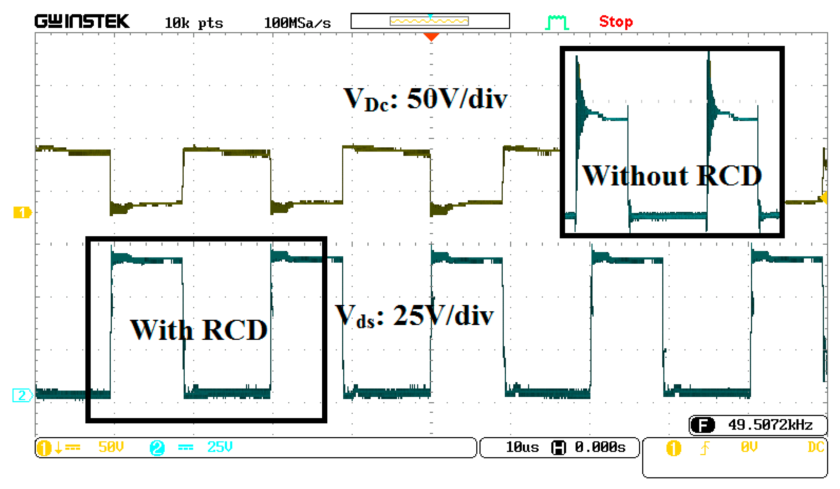
  • The converter is provided with the traditional RCD clamp circuit to reduce the voltage stress of the MOSFET switch.
  • Performance comparison and design guidelines of the proposed converter is discussed in detail.
  • The mathematical equations of the output voltage under ideal and practical conditions are discussed for better insight.
  • Finally, the circuit structure with an active clamp circuit is also proposed in this paper as a future extension.
The organization of the paper as follows: Section 2 discusses the system configuration and operation of the proposed converter in CCM, DCM, and BCM. The steady-state analysis of the proposed converter in addition to the voltage and current stresses of various devices is discussed in Section 3, and design guidelines and performance comparison are carried out in Section 4. Section 5 discusses the simulation and experimental results of the proposed converter in CCM operation. The paper is concluded in Section 6.

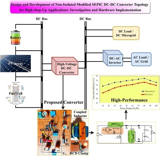
2. System Configuration

Figure 1a depicts the structure of the proposed converter and Figure 1b shows the equivalent circuit of the proposed converter. In Figure 1b, the variables of the proposed converter are illustrated, in which, the current through the MOSFET switch is represented as Ids, the current the primary and secondary of the coupled inductor is represented as ILp and ILs, respectively, the leakage current of the coupled inductor is represented as ILlk, the current through the diodes, such as D1, D2, and D3 are represented as ID1, ID2, and ID3, the voltage stress of MOSFET is denoted as Vds, and the load current is represented as Iout. The operating principle of the proposed converter in CCM and DCM is illustrated, and the operation in boundary conduction mode (BCM) is also briefly introduced. The proposed converter in this paper resembles the basic SEPIC converter with two additional diodes and splitting the output capacitor into two equal capacitors.

2.1. CCM Operation

It is noticed from Figure 1 that the converter topology does not need an isolated drive circuit for the MOSFET, which results in less cost. Besides, the capacitor, C, is connected in series with the coupled inductor, which stops the dc current flow in the coupled inductor and hence avoids saturation. Several assumptions are made to analyze the converter operation, which can be given as follows: (i) Diodes and MOSFET are considered as ideal devices, (ii) the value of the capacitors are large enough to produce ripple-free voltage, and (iii) the effects of leakage inductance are negligible, and the coupled inductor is modelled as an ideal transformer with a turns ratio T2/T1. The theoretical waveform of the proposed converter in CCM operation is illustrated in Figure 2. The operating modes are split into three modes for better understanding:
Mode-1 (tt1): AT t = t0, the MOSFET switch is ON, the diodes D1, D2 are reverse biased and the diode D3 is forward biased. During this mode, the capacitor C delivers energy to the load along with the secondary side of the coupled inductor. The output capacitors such as Cox, Coy gets charged during this period. The magnetizing current reaches its maximum value at the end of this mode. The voltage across the magnetizing inductor Lm is equal to the input source voltage, Vin, and this mode ends at t = t1. The current directions are depicted in Figure 3a.
Mode-2 (t1t2): AT t = t1, the MOSFET switch is OFF, the diodes D2 and D3 are reverse biased and the diode D1 is forward biased. During this mode, the leakage energy delivered by the coupled inductor is recovered using the RCD clamp circuit, and the voltage stress across the switch can be reduced. The diode, D1, provides the path for the magnetizing current, and the output capacitors, Cox, and Coy delivers the required power to the load. This mode is very short, and this mode ends at t = t2. The current directions are depicted in Figure 3b.
Mode-3 (t2t3): AT t = t1, the MOSFET switch is turned off, the diodes D1, D2 are forward biased and the diode D3 is reverse biased, which provides the path for the magnetizing current. During this mode, the output capacitors such as Cox, Coy delivers power to the load. At t = t3, when the switch is turned on again, this mode ends. The current directions are depicted in Figure 3c.

2.2. DCM Operation

Similar to CCM operation, the DCM has three modes of operation, and the operation of the converter in DCM during the first two modes are similar to CCM. The key waveform of the proposed converter under DCM operation is shown in Figure 4. The current path of the third operating mode of the proposed converter is shown in Figure 5.
During the third mode of converter operation, the diodes such as D1, D2, and D3 are reverse biased and the MOSFET switch is already in OFF state. The magnetizing current of the primary of the coupled inductor is circulated, as shown in Figure 5. At the end of this mode, the MOSFET switch is turned ON again and the cycle repeats. Practically, the converters are not allowed to operate in DCM operation due to its features such as discontinuous current, and low conversion efficiency. Moreover, the converter voltage gain is load dependent during DCM operation. Therefore, the converter under DCM operation is not recommended for any applications.

3. Steady-State Analysis of the Proposed Converter

The steady-state analysis of the proposed converter is analyzed in this section of the paper. For the investigation, the converter operation during one switching period is considered. For ease of analysis, the effect of the parasitic elements of the components is neglected to derive the expression for the static voltage gain of the proposed converter in this section. Later, the effects of parasitic elements of various components are discussed. The operation of the proposed converter is very short during Mode-2, and therefore, the converter operation during Mode-2 is not considered for steady-state analysis.
During Mode-1 (from Figure 3a), the voltage across the magnetizing inductor of the coupled inductor (VLm) is equal to the input source voltage (Vin), as presented in Equation (1):
V L m I = V i n
During Mode-3 (from Figure 3c), the expression for the voltage across the magnetizing inductor is derived by applying Kirchhoff’s voltage law (KVL) and is given in Equation (2):
V L m I I I = V i n V C 1 + T
By using the voltage-second balance principle over one switching period of the converter, the following condition is derived:
D V i + ( 1 D ) ( V i n V C ) 1 + T = 0
where, the turns ratio of the coupled inductor, T = T2/T1, and the voltage across the coupling capacitor, C is as follows:
V C = 1 + T D 1 D V i n
Since the output capacitor is split into two halves, the voltage across the two capacitors such as VCox and VCoy needs to be derived during the converter operation. By applying KVL during Mode-1, the voltage across the capacitor, Cox is obtained as:
V C o x = V C + T V i n = ( 1 + T ) V i n 1 D
Similarly, by using KVL during Mode-3, the voltage across the capacitor, Coy is derived as:
V C o y = V i n D T 1 D
The voltage across the capacitor can supply the converter load. Therefore, the output voltage (Vo) of the proposed converter is equal to the sum of the voltage across the capacitors, such as VCox and VCoy, and is given in Equation (7):
V o u t = V C o x + V C o y = ( 1 + T ) V i n + V i n D T 1 D
The static voltage gain, M of the proposed converter is derived from Equation (8) as follows:
M C C M = V o u t V i n = 1 + T + D T 1 D
The voltage gain of the proposed converter for various values of turn’s ratio of the coupled inductor is depicted in Figure 6. From Figure 6, it is observed that the voltage gain can be increased by increasing the turn ratio.
The converter proposed in this paper may also operate in BCM when the magnetizing current of the coupled inductor, iLm reaches zero during the next switching period. Figure 7 depicts the key waveform for the magnetizing voltage and its respective current. The converter enters into BCM due to reasons such as the value of Lm is a small or less loading condition or switching frequency, fs is low. From Figure 7, the expression for the magnetizing inductor current ripple and the average value of the magnetizing inductor current are derived as follows:
Δ i L m = V i D T s L m
i L m = Δ i L m 2 = V i n D T s 2 L m
Due to the series-connected capacitor with the secondary winding of the coupled inductor, the primary side and secondary side average values of the current is equal to zero. Therefore, by applying Kirchhoff’s current law, the average value of the input current is derived as follows:
i i = i L m
By neglecting the effect of parasitic elements of the components, the output power of the converter is assumed to equal to the input power:
V i n I i n = V o u t I o u t
Substitute Equation (8) and Equations (10)–(11) in Equation (12) and Equation (12) is modified as follows:
V i n D T s 2 L m = 1 + T + D T 1 D I o u t ( b o u n d a r y )
From Equation (13), the boundary value of the output current (Io(boundary)) and the normalized boundary value of the output current are simplified as follows:
I o u t ( b o u n d a r y ) = D ( 1 D ) 2 V o u t 2 L m f s ( 1 + T + T D ) 2
I o u t ( b o u n d a r y ) V o u t 2 L m f s = D ( 1 D ) 2 ( 1 + T + T D ) 2
From Equation (14), the expression for the magnetizing inductance is derived and presented in Equation (16). This is the minimum value of the magnetizing inductance (Lm) to maintain the converter operation in CCM, and the converter goes to DCM operation if the value of Lm is small. In addition, the boundary value of the output load resistance is given in Equation (17):
L m D ( 1 D ) 2 V o u t 2 I 0 u t ( b o u n d a r y ) f s ( 1 + T + T D ) 2
R o ( b o u n d a r y ) = 2 f s L m ( 1 + T + T D ) 2 D ( 1 D ) 2
As discussed earlier, the converter goes to DCM operation if the value of load resistance is small, as presented in Equation (17). The plot between the normalized boundary output current and the duty cycle of the switch for various turns ratio of the coupled inductor is illustrated in Figure 8. It is observed from Figure 8 that the CCM operating region of the converter can be increased by increasing the turn’s ratio. As discussed earlier, the converter enters into DCM operation if it crosses the boundary, as shown in Figure 8. When the converter in DCM operation, the average value of the inductor magnetizing current is derived as follows:
i L m = Δ i L m ( D + D c ) 2 = V i n D ( D + D c ) T s 2 L m
where, DcTs is the time to reach zero value from the maximum value by the magnetizing inductor current.
Equation (19) is derived from Equations (11) and (12) for obtaining the expression for the duty cycle of the switch during DCM operation:
V i n 2 D ( D + D c ) 2 f s L m = V o u t 2 R o
By applying the volt-second balance principle as similar to Equation (3), the following expression is derived:
D V i n + D c ( V i n V C ) 1 + T = 0
From Equations (3), (4) and (20), the voltage gain of the proposed converter under DCM operation is obtained as follows:
M D C M = V o u t V i n = ( 1 + T ) D c ( T D ( 1 D ) + ( 1 + T D ) D c 1 D ) = D ( D + D c ) 2 τ s
where, the normalized time constant is represented as τs and is presented in Equation (22). In addition, the expression for the duty cycle Dc is derived as follows:
τ s = L m R o T s
D c = D ( 1 + T ) V i n V o u t V i n ( 1 + T )
From Equation (21), it is observed that the voltage gain of the proposed converter during DCM operation is load-dependent, and usually, the converter under DCM is not preferable for any practical applications.

Voltage Stress and Current Stress of MOSFET and Diodes

Apply KVL in Figure 2c to derive the voltage stress of the MOSFET switch during Mode-3 of CCM operation. The MOSFET voltage stress is derived as follows:
V d s = V i n V L m I I I = V i n ( V i n V C ) 1 + T = V i n 1 D = V o u t 1 + T + T D
From Equation (24), it is noticed that the voltage stress of the MOSFET switch is very much less than the output voltage of the converter. The switching power loss of the MOSFET switch is derived as follows, in which the intrinsic capacitance of the MOSFET switch is represented as Cs:
P s w = f s C s V d s 2 = f s C s V i n 2 ( 1 D ) 2
From Equation (25), it is noticed that the switching loss of the proposed converter is less than the conventional SEPIC converter. Besides, it enables the researcher to select the low voltage rating MOSFET switch with low on-state resistance (rds-on) for the switching operation, which further reduces the conduction loss and hence the efficiency. The voltage stress of the diodes, such as VD1, VD2, and VD3, is derived as follows:
V D 1 = 1 + T 1 D V i n
V D 2 = V D 3 = T V i n 1 D
The average value of MOSFET current is equal to the average value of the magnetizing inductor current. In addition, the average value of magnetizing inductor current is equal to the average value of the input current, and this is due to the average value of the primary side inductor current is equal to zero. By considering all these facts, the current stress of the MOSFET switch is derived and is given in Equation (29):
I d s = I L m = I i n = 1 + T D 1 D I o u t
I d s = ( 1 + T D ) D ( 1 D ) I o u t
The current stress of all the diodes is derived as follows:
I D 2 = I D 3 = I o u t / D
I D 1 = I o u t / ( 1 D )
From the above discussions, it is noticed that the voltage stress across the switch and diodes is lower than half of the output voltage of the proposed converter. Therefore, the switch with low on-state resistance has been selected for the proposed converter resulting in less conduction loss with high conversion efficiency.

4. Design Guidelines and Performance Comparison of the Proposed Converter

4.1. Design Guidelines

The specifications of the proposed converter are presented in Table 1 and based on the specifications; an experimental prototype is made to validate the performance of the proposed converter.
From Equation (8), the minimum and maximum value of the duty cycle of the switch as follows:
D m i n = 1 [ ( 1 + T + T D ) V i , m a x V 0 ] = 0.4
D m a x = 1 [ ( 1 + T + T D ) V i , m i n V 0 ] = 0.6
The optimal value of the duty cycle is 0.5, and therefore the proposed converter is switched at 0.5 duty cycle for the optimal duty cycle. From Equation (24), the voltage stress of the MOSFET switch is equal to 50 V, and the value of the maximum current stress of the switch is calculated as follows:
I d s , m a x = ( 1 + T D m a x ) D m a x ( 1 D m a x ) [ I o u t ] = 4.58   A
Based on the above discussions, the voltage and current rating of the MOSFET should be more than 50 V and 4.58 A, and therefore, a MOSFET IRFB4410 with 100 V, and 96 A rating is selected for the proposed converter. The minimum value of the magnetizing inductance is calculated by substituting the minimum value of the duty cycle of the switch in Equation (16), and is presented in Equation (35). If the value of the magnetizing inductance is less than the value calculated using Equation (35), the converter operation goes to DCM:
L m 0.4 ( 1 0.4 ) 2 × 200 2 × 0.5 × 50000 × ( 1 + 2 + ( 2 0.4 ) ) 2 = 39.58   μ H
By using Equation (35), the minimum value of the magnetizing inductance is calculated and is found equal to 39.58 µH. The value is selected as 200 µH to maintain the converter operation in CCM. Finally, the coupled inductor is designed with EI33 ferrite core by considering the values T = 2, and Lm = 200 µH for the CCM operation. Similarly, the voltage stress of the diodes such as VD1, VD2, and VD3 is calculated using Equations (26) and (27) and is equal to 150 V, 100 V, and 100 V, respectively. In addition, the current stress of the diodes such as ID1, ID2, and ID3 is calculated using Equations (30) and (31), and is equal to 1 A, 1 A, and 1 A, respectively. By considering all the facts, a Schottky diode (MUR820) with rating 200 V, 8 A, has been selected for the converter operation. The value of the output capacitor (Co) is calculated using Equation (36), and is given below:
C 0 = ( 1 D m a x ) I 0 u t f s Δ V C = ( 1 0.6 ) × 0.5 50000 × 1.1 = 3.63   μ F
In the proposed converter, the output capacitor is split into two equal parts, and the output capacitance, such as Cox and Coy is equal to 20 µF. Therefore, the output capacitors such as Cox and Coy are selected as 22 µF, 250 V (electrolytic type) each. The minimum value of the capacitor, C, can be calculated using Equation (16):
C m i n I 0 u t f s Δ V C = 0.5 50000 × 1.1 = 9.09   μ F
The value of the coupling capacitor, C, is calculated as 9.09 µF, and for ripple-free operation, 10 µF, 250 V electrolytic capacitor has been selected. The values of the resistor and the capacitor in the RCD clamp is selected based on the literature [38,39]. In the proposed converter, the peak voltage of the MOSFET switch is clamped, which should satisfy the following equation:
V d s s > V i n + V C c
where, the breakdown voltage of the MOSFET switch is represented as Vdss, and the voltage across the clamp capacitor, Cc, is represented as VCc. The voltage ripple in the clamp capacitor voltage is negligible by selecting a large value for the clamp capacitor, i.e., C c > T s / R c , where Ts is switching period, and the clamp resistance is represented as Rc. This breakdown voltage increases until the power dissipated the clamp resistor, PRc is equal to the average leakage inductance power transfer, PLlk:
P L l k = W L l k T s = P R c = 1.63 × 10 6 × 50 × 10 3 = 81.92   mW
W L l k = 1 2 L l k I d s 2 = 1.63   μ J
The voltage across the clamp resistance during the off period of the switch must satisfy the following equation:
V R c = V C c = ϑ × V d s , m a x V i n = ( 0.8 × 50 ) 25 = 15   V
where, ʋ is voltage security constant and is usually equal to 0.8–0.95. Moreover, now, the expression for the clamp resistance and the clamp capacitance is derived as follows:
R c = V R c 2 P L l k = 15 2 81.92 × 10 3 3.3   k Ω
C c > T s / R c 6   nF

4.2. Performance Comparisons

The converter proposed in this paper is compared with the traditional SEPIC dc-dc converter with the coupled inductor [23]. In addition, the voltage gain of various converters is plotted in Figure 9. The performance comparison is also presented in Table 2. As seen in Figure 9, the voltage gain of the proposed converter is higher than the traditional SEPIC converter proposed in [23] by adding an extra two diodes and one capacitor with the traditional one. In addition, as seen in Table 2, the voltage stress of the switch in the proposed converter is much less than the conventional converter when the turn’s ratio of the coupled inductor is higher than one, which also helps to select the MOSFET switch with low rds-on. This helps the converter to achieve high conversion efficiency by minimizing the switching and conduction losses.
The proposed converter is also compared with the other converter topologies, which is employed with the coupled inductors. However, the converters with a high-boosting technique such as VM cells, voltage lift, quadratic boost, cascaded connections are not considered for the comparison. To have a fair performance comparison, the converter with two winding coupled inductor with a single MOSFET switch is taken into account. Therefore, the proposed converter is compared with nine other converter topologies in terms of voltage gain, a number of components, and voltage stress of the switch.
From Table 2, it is witnessed that the proposed converter holds a better position in terms of a device count, MOSFET voltage stress, and the voltage gain when compared to other converters except the converter presented in [24]. The voltage gain of the proposed converter and the converter proposed in [24] is similar; however, the proposed converter has one diode and one capacitor less in number. Moreover, the voltage gain is four times better than the traditional coupled inductor based SEPIC converter.

4.3. Efficiency and Power Loss Analysis

The analysis of the converter efficiency is discussed in this section of the paper. The equivalent circuit of the proposed converter, including the internal resistance of each component is illustrated in Figure 10, in which, r L p and r L s are the coupled inductor’s primary and secondary Equivalent Series Resistance (ESR), respectively. Similarly, the internal resistance of the diodes are denoted as r D c , r D 1 , r D 2 , and r D 3 and its respective forward voltage drop is represented as V F D c , V F D 1 , V F D 2 , and V F D 3 . The conducting duration of the clamp diode is very less, and therefore, the effect of the clamp diode parasitic element and the voltage drop is neglected in this paper. The on-state resistance of the MOSFET switch is represented as r d s .
The voltage equation of two sides of the coupled inductor by considering the parasitic elements in nonconducting and conducting states are given as follows:
V L p = V i n I L p ( r L p + r d s ) V L s = V C + V C o x I L s ( r L s + r D 3 ) V F D 3 V o u t + V C o y }   ON   State
V L p = V i n I L p ( r L p + r L s + r D 1 ) V F D 1 V C V L s = V C V C o x I L s ( r L s + + r D 2 ) V F D 2 + V o u t + V C o y }   OFF   State
The output voltage of the proposed converter is derived by applying the volt-second balance principle by considering the components voltage drop and is presented as follows:
V o u t = V i n ( 1 + T + D T ) 1 D [ A r L p + B r L s + C r d s + E r D 1 + F r D 2 + G r D 3 ]
where, A = V i n ( 1 + T D ) 2 R o ( D ( 1 D ) ) 2 , B = D V i n R o , C = V i n ( 1 + T D ) R o D ( 1 D ) ( ( 1 D ) + 1 + D ( 2 D ) ) , E = V i n R o ( 1 D ) ( D 2 + V D 1 ) , F = V i n R o D ( D 2 + V D 1 ) , and G = V i n R o D ( ( 1 D ) + V D 3 ) . From above all equation, it is worth noticing that the voltage drop of the MOSFET switch is high as compared to diodes and the voltage drop of the diode, D3 and the secondary of the coupled inductor is less at 50% duty cycle. The converter efficiency and the output voltage gain are affected by the switching loss of the MOSFET and the conduction loss of the various components. The expression for the converter efficiency is given in Equation (47). The efficiency of the proposed converter is analyzed by calculating the power losses of the circuit elements. The converter efficiency is calculated as follows:
η = P o u t P o u t + P l o s s = P o u t P o + P l o s s S + P l o s s C + P l o s s C I + P l o s s D
where, P o u t is the output power of the converter, P l o s s S is the loss due to the MOSFET switch, P l o s s C is the loss due to the capacitors, P l o s s C I is the loss due to the coupled inductor, and P l o s s D is the loss due to the diodes. The MOSFET power loss is equal to the sum of the switching loss ( P S W l o s s S ) and the conduction loss ( P c l o s s S ) and the expression is given as follows:
P l o s s S = P S W l o s s S + P c l o s s S = 1 2 V d s I d s ( t f + t r ) f s + r d s I d s 2
where, t f and t r are falling and rising time of the MOSFET switch and the switching frequency is represented as fs. From above all equations, the expression for the power losses of the MOSFET switch is given as follows:
P S W l o s s S = 1 2 V i n 1 D × V o u t ( 1 + T D ) R o ( 1 D ) ( t f + t r ) f s
P c l o s s S = r d s × [ V o u t ( 1 + T D ) R o ( 1 D ) ] 2
The expression to calculate the loss of each diode, capacitors, and the coupled inductor are as follows:
P l o s s D = V F × I D + ( r D × I D ( r m s ) 2 )
P l o s s C = r C × I C ( r m s ) 2
P l o s s C I = r L × I L ( r m s ) 2
where VF is the forward voltage drop of the diode, rD is the ESR of the diode, rC is the ESR of the capacitors, and the rL is the ESR of the coupled inductor.

5. Results and Further Discussion

To validate the theoretical analysis of the proposed converter, the converter is first simulated and also verified with the experimental results in further sub-sections. The simulations and experimentations were carried-out by considering the various parameters listed in Table 1.

5.1. Simulation Results

To validate the performance of the proposed converter, the simulations are carried out using MATLAB/Simulink software, and various simulation waveforms are illustrated in Figure 11. The simulation is carried out at full load condition. To get the required voltage gain, the duty cycle of the MOSFET switch of adjusted to 0.5. The load resistance, R0 is selected as 400 Ω, 2 A. The electrical specifications of the proposed converter, the values of capacitance and the coupled inductor inductances are listed in Table 1.
The gate-source voltage and the voltage stress of the MOSFET switch are shown in Figure 11a, and from Figure 11a, it is noticed that during Mode-2, the maximum voltage stress is about 60 V, and during Mode-3, the maximum voltage stress about 50 V, as discussed earlier. The remaining 10 V is clamped using the RCD clamp circuit, and the voltage stress across the clamp diode (VDc) is shown in Figure 11c. The maximum current stress of the MOSFET switch at a 0.5 duty cycle is calculated using Equation (29), and is equal to 4 A. The same can be noticed from Figure 11b. During the OFF time of the MOSFET switch, the voltage stress of the clamp diode is equal to the voltage stress of the MOSFET switch. Figure 11d illustrates the current waveforms of the diode D1 and the diode, Dc. It is observed from Figure 11d that the current stress of the diode, ID1 is equal to 1 A and the same can be calculated using Equation (31). It is also noticed that the clamp diode clamps the leakage energy during mode-2 and the current stress of the clamp diode, IDc is observed as 0.78 A. The voltage stress of the diodes such as VD1, VD2, and VD3 are calculated using Equations (26) and (27), and is equal to 150 V, 100 V, and 100 V, respectively. The same can be observed in waveforms, as depicted in Figure 11e,f. The average value of the current stress of the diodes, such as ID2 and ID3, is calculated using Equation (30), and is equal to 1 A and 1 A, respectively. The same can be observed in waveforms, as depicted in Figure 11g. The voltage across the capacitors such as VC, VCox, and VCoy, and calculated using Equations (4)–(6), and is equal to 100 V, 150 V, and 50 V, respectively. The same can be observed in Figure 11h. The output voltage, Vout of the proposed converter is equal to the sum of the voltage across the capacitors, VCox and VCoy, and is equal to 200 V. The same can be observed in Figure 11i for the input voltage, Vin is equal to 25 V. All the simulation waveforms are in good agreement with the theoretical discussions, as presented in Section 2 of this paper. Therefore, the performance of the proposed converter is validated using simulations.

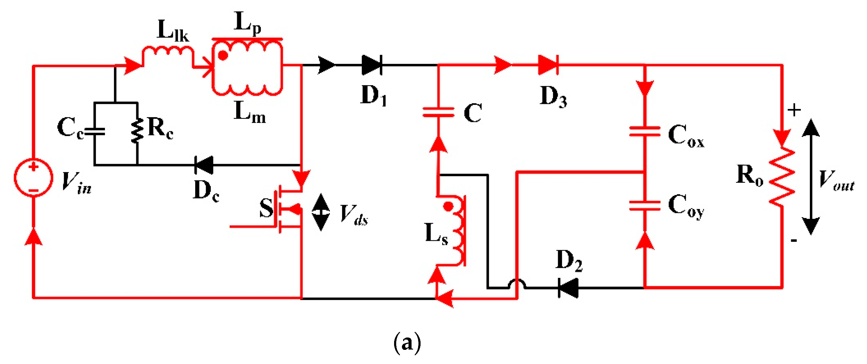
5.2. Hardware Results

As per earlier discussions, and specification, a 100 W, 200 V/0.5 A, an experimental prototype of the proposed converter is fabricated, and tested in the laboratory environment to validate the performance experimentally. The duty cycle of the switch is kept at 0.5 to get the required output voltage at T = 2, and Vin = 20 V. Table 3 shows various components of the proposed converter and its specifications. Figure 12 depicts the experimental prototype.
Figure 13 illustrates the experimental waveforms under full load conditions. The waveforms for gate-source voltage (Vgs) and the voltage stress of the MOSFET switch is illustrated in Figure 13a. The gate-source voltage is produced using the MSP430FR2355 Texas Instruments development board, and this PWM pulse is isolated and MOSFET driven with the help of TLP250 MOSFET/IGBT gate driver IC. The voltage sensor, LV-55-P, senses the output voltage of the proposed dc-dc converter, and this feedback is processed through MATLAB/Simulink for effective closed-loop operation of the converter. By assuming a 1% output ripple voltage, the capacitance of the output capacitors VCox and VCoy are selected. From Figure 13a, it is noticed that the voltage stress of the MOSFET switch is about 60 V and the leakage energy of the coupled inductor is effectively clamped using the passive RCD clamp circuit. Figure 13b shows the waveform of the voltage stress and current stress of the MOSFET switch. The current stress of the MOSFET switch is observed as 4.56 A and voltage stress is observed as 60 V, which almost satisfies the theoretical values. Besides, it is also noticed that the MOSFET switch is operated at zero-voltage switching condition, which minimizes the switching losses of the MOSFET. The waveform of the voltage across the clamp diode is depicted in Figure 13c. From Figure 13c, it is observed that the clamp diode effectively clamps the leakage energy during Mode-2 of the converter operation and the voltage stress of the clamp diode is similar to the voltage stress of the MOSFET switch. The waveforms for the current stress of the clamp diode, iDc, and the current stress of the diode, D1 is depicted in Figure 13d. It is noticed that the clamp diode clamps the leakage energy of the coupled inductor during Mode-2 and the current stress of the clamp diode is observed as 0.75 A. Similarly, the current stress of the diode, D1 is observed as 1.05 A. The voltage stress of the various diodes is depicted in Figure 13e,f. As per the earlier discussions, the maximum voltage stress of the diodes such as VD1, VD2, and VD3 is equal to 150 V, 100 V, and 100 V, respectively. The same can be noticed from Figure 13e,f, and the voltage stress is somewhat deviated from the actual due to the parasitic elements of the diodes. The current stress of the diodes, such as iD2 and iD3, is illustrated in Figure 13g. By using Equations (30) and (31), the average current stress of the diodes such as iD2, and iD3 are equal to 1 A, and 1 A, respectively, and the same can be noticed from Figure 13g. The maximum voltage across the capacitors such as VC, VCox, and VCoy is equal to 100 V, 150 V, and 50 V, respectively. From Figure 13h, it is observed that the voltage across the capacitors is equal to 98 V, 146 V, and 51 V, respectively, and this deviation is due to the parasitic elements of the capacitors. The input source current, ii, and the input source voltage are illustrated in Figure 13i, and from Figure 13i, it is observed that the source current is continuous throughout the operating period of the converter when the converter is operated at CCM operation, which proves the theoretical discussion. The waveforms of the input source, Vin, and the output voltage, Vout of the proposed converter is illustrated in Figure 13j. The input source voltage is kept constant at 25 V, and the output voltage of the converter is observed as 199 V from Figure 13j. It is also noted that as per the electrical specifications, the proposed converter can deliver the required voltage gain of 8 at the duty cycle of 50%.
It is noticed from various waveforms that the proposed converter is employed with the passive RCD clamp circuit in the primary of the coupled inductor to reduce the leakage inductance effect and to prevent the MOSFET switch from the voltage spikes/oscillations. To highlight the usage of the clamp circuit, the waveform for the voltage stress of the MOSFET switch with and without the clamp circuit is illustrated in Figure 14. It is observed from Figure 14 that the maximum magnitude of the switch voltage spike is greater than 100 V, and is lesser than the output voltage of the converter without the RCD clamp circuit.
At the same time, the maximum magnitude of the switch voltage spike is less than 60 V and is lower than the output voltage of the converter with the RCD clamp circuit. It is concluded that the passive RCD circuit effectively clamps the voltage spikes and helps to maintain less voltage stress of the MOSFET switch.
From the above discussions and various waveforms, it is concluded that the proposed converter is performing as per the theoretical analysis and the simulation results, and the performance of the proposed converter is better than the converter presented in the literature. The power losses in the proposed converter are analyzed by neglecting the switching losses since the MOSFET switch operates at the zero-voltage-switching condition. Moreover, the diode reverse-recovery losses are omitted due to the consideration of the coupled inductor leakage inductance. Thus, the overall losses of the proposed converter include conduction losses and the coupled inductor losses. The power loss distribution of the proposed converter is presented in Table 4.
The performance characteristics of the proposed converter are shown in Figure 15. It is observed that the maximum efficiency of the proposed converter is 95.1% and the full load efficiency of the converter is 93.83%.
The various experimental values of the proposed converter are compared with the simulation values and the theoretical values, and the same has been presented in Table 5. The result proves that experimental values are nearly equal to theoretical and simulated values. From Table 5, it is observed a few variations in the voltage stress of the switch and diodes, and this is due to the parasitic components such as parasitic inductance, on-state resistance, and parasitic capacitance.
The cost analysis of the proposed converter is listed in Table 6 for two different power ratings, such as 100 W and 1 kW [44]. It is clearly observed from Table 6 that the cost of the proposed converter reduces when the rating of the converter increases. The cost of the proposed converter is also compared with the other similar converters proposed in the literature and is presented in Table 7. From Table 7, it is noticed that the proposed converter holds a better cost position with respect to a high voltage gain capability along with an excellent conversion efficiency. The conversion efficiency of the proposed converter may be improved by proper design of the coupled inductor since the power losses supplied by the coupled inductor is more than 40% of the total power losses. Besides, the efficiency also increased by replacing the passive clamp circuit by the active clamp circuit if the rating is more than 500 W. However, for a low power application (say, <500 W), the proposed converter with RCD clamp circuit holds a better position in terms of cost, whereas, for the rating above 500 W, it is suggested to go with the active clamp circuit to have better conversion efficiency. The extension of the proposed converter with the active clamp circuit is also presented in Figure 16 for the researchers as a future extension and the same has been derived from [45]. However, the operation of the converter is similar to the previous discussions.

6. Conclusions

A new modified SEPIC dc-dc boost converter topology is proposed and discussed in this paper. The operation of the proposed converter is theoretically analyzed in both CCM and DCM modes. The proposed converter has advantages such as less voltage stress of the switch, and diodes, less output voltage ripple, and high conversion efficiency. The expressions for the static voltage gain, voltage and current stresses of various components are derived. In addition, the expression for the output voltage with non-idealities and design guidelines are given sequentially. The conventional RCD clamp circuit has been used to reduce the voltage stress of the switch, and it helps to select the MOSFET with low rds-on, which reduces the conduction losses. Also, the loss due to device switching is diminished by the zero-voltage-switching technique. Therefore, the power loss of the proposed converter is less and hence increases the conversion efficiency. The proposed converter is compared with the similar converter topologies and concluded that the proposed converter has better voltage gain with less number of components. This feature enables the researcher to select the compact and high reliable converter for real-time applications. The maximum efficiency of the proposed converter is 95.2% at 80 W, and the full load efficiency is 93.83% at 100 W. Finally, it can be concluded that the proposed converter is best suitable for high voltage renewable energy systems.

Author Contributions

M.P. was originally responsible for conceptualization, methodology, simulation, experimentation and prepared the original draft of the article. U.S. verified the simulation data, experimental draft writing, and also provided technical guidance. H.H.A. and P.S. made a formal analysis of the technical write-up, review, editing, and supervision. All authors have read and agreed to the published version of the manuscript.

Funding

This research did not receive any specific grant from funding agencies in the public, commercial, or not-for-profit sectors.

Acknowledgments

The authors extend their thankfulness to GMR Institute of Technology, Rajam, Andhra Pradesh, India, for providing facility and allowing us to validate the performance of the system at the power electronics laboratory.

Conflicts of Interest

The authors declare no conflict of interest.

References

  1. Premkumar, M.; Kumar, C.; Sowmya, R. Analysis and implementation of high-performance DC-DC step-up converter for multilevel boost structure. Front. Energy Res. 2019, 7, 149. [Google Scholar] [CrossRef] [Green Version]
  2. Premkumar, M.; Kumar, C.; Anbarasan, A.; Sowmya, R. A novel non-isolated high step-up DC-DC boost converter using single switch for renewable energy systems. Electr. Eng. 2020, 102, 811–829. [Google Scholar] [CrossRef]
  3. Premkumar, M.; Subramaniam, U.; Babu, T.S.; Elavarasan, R.M.; Mihet-Popa, L. Evaluation of mathematical model to characterize the performance of conventional and hybrid PV array topologies under static and dynamic shading patterns. Energies 2020, 13, 3216. [Google Scholar] [CrossRef]
  4. Gules, R.; Dos Santos, W.M.; Dos Reis, F.A.; Romaneli, E.F.R.; Badin, A.A. A modified SEPIC converter with high static gain for renewable applications. IEEE Trans. Power Electron. 2014, 29, 5860–5871. [Google Scholar] [CrossRef]
  5. Madurai Elavarasan, R.; Ghosh, A.; Mallick, T.K.; Krishnamurthy, A.; Saravanan, M. Investigations on performance enhancement measures of the bidirectional converter in PV—wind interconnected microgrid system. Energies 2019, 12, 2672. [Google Scholar] [CrossRef] [Green Version]
  6. Maroti, P.K.; Padmanaban, S.; Holm-Nielsen, J.B.; Pecht, M.; Ojo, O. A novel configuration of modified Cuk converter using multiple VLSI modules for high voltage renewable energy application. In Proceedings of the 45th Annual Conference of the IEEE Industrial Electronics Society, Lisbon, Portugal, 14–17 October 2019; pp. 4083–4088. [Google Scholar]
  7. Maroti, P.K.; Bhaskar, M.S.; Padmanaban, S.; Holm-Nielsen, J.B.; Sutikno, T.; Iqbal, A. A new multilevel member of modified Cuk converter family for renewable energy applications. In Proceedings of the IEEE Conference on Energy Conversion, Yogyakarta, Indonesia, 16–17 October 2019; pp. 224–229. [Google Scholar]
  8. Shokati, A.E.; Sabahi, M. Bidirectional quasi-Cuk dc/dc converter with reduced voltage stress on capacitor and capability of changing the output polarity. J. Electr. Eng. Technol. 2017, 12, 1108–1113. [Google Scholar]
  9. Narula, S.; Singh, B.; Bhuvaneswari, G. Power factor corrected welding power supply using modified zeta converter. IEEE J. Emerg. Sel. Top. Power Electron. 2016, 4, 617–625. [Google Scholar] [CrossRef]
  10. Maroti, P.K.; Padamanaban, S.; Bhaskar, S.M.; Holm–Nielsen, J.B.; Blaabjerg, F.; Lonel, D.M.; He, J.B. A non-isolated inverting high gain modified new series of landsman converter. In Proceedings of the 45th Annual Conference of the IEEE Industrial Electronics Society, Lisbon, Portugal, 14–17 October 2019; pp. 4077–4082. [Google Scholar]
  11. Ajami, A.; Ardi, H.; Farakhor, A. A novel high step-up DC/DC converter based on integrating coupled inductor and switched-capacitor techniques for renewable energy applications. IEEE Trans. Power Electron. 2015, 30, 4255–4263. [Google Scholar] [CrossRef]
  12. Wai, R.J.; Jheng, K.H. High-efficiency single-input multiple-output dc-dc converter. IEEE Trans. Power Electron. 2013, 28, 886–898. [Google Scholar] [CrossRef]
  13. Zhao, Q.; Lee, F.C. High-efficiency, high step-up dc-dc converters. IEEE Trans. Power Electron. 2003, 18, 65–73. [Google Scholar] [CrossRef] [Green Version]
  14. Shahir, M.; Babaei, E.; Farsadi, M. Analysis and design of voltage-lift technique-based non-isolated boost dc-dc converter. IET Power Electron. 2018, 11, 1083–1091. [Google Scholar] [CrossRef]
  15. Zhou, M.; Yang, M.; Wu, X.; Fu, J. Research on composite control strategy of quasi-z-source dc-dc converter for fuel cell vehicles. Appl. Sci. 2019, 9, 3309. [Google Scholar] [CrossRef] [Green Version]
  16. Schmitz, L.; Martins, D.C.; Coelho, R.F. High step-up non-isolated ZVS/ZCS DC-DC converter for photovoltaic thin-film module applications. IEEE J. Emerg. Sel. Top. Power Electron. 2019, 7, 565–575. [Google Scholar] [CrossRef]
  17. Ting, N.S.; Sahin, Y.; Aksoy, I. Analysis, design, and implementation of a zero-voltage-transition interleaved boost converter. J. Power Electron. 2017, 17, 41–55. [Google Scholar] [CrossRef] [Green Version]
  18. Harchegani, A.T.; Mahdavi, M. A new soft-switching dual input converter for renewable energy systems. J. Power Electron. 2017, 17, 1127–1136. [Google Scholar]
  19. Moradzadeh, M.; Babaei, E.; Zamiri, E.; Hamkari, S. A new high step-up dc/dc converter structure by using coupled inductor with reduced switch-voltage stress. Electr. Power Compon. Syst. 2017, 45, 1705–1719. [Google Scholar] [CrossRef]
  20. Tang, Y.; Wang, T.; He, Y. A switched-capacitor-based active network converter with high voltage gain. IEEE Trans. Power Electron. 2013, 29, 2959–2968. [Google Scholar] [CrossRef]
  21. Tran, D.; Chakraborty, S.; Lan, Y.; Van Mierlo, Y.; Hegazy, O. Optimized multiport dc/dc converter for vehicle drivetrains: Topology and design optimization. Appl. Sci. 2018, 8, 1351. [Google Scholar] [CrossRef] [Green Version]
  22. Gao, W.; Zhang, Y.; Lv, X.; Lou, Q. Non-isolated high-step up soft-switching DC/DC converter with low-voltage stress. IET Power Electron. 2017, 10, 120–128. [Google Scholar] [CrossRef]
  23. Park, K.B.; Moon, G.W.; Youn, M.J. Non isolated high step-up boost converter integrated with SEPIC converter. IEEE Trans. Power Electron. 2010, 25, 2266–2275. [Google Scholar] [CrossRef]
  24. Hsieh, Y.P.; Chen, J.F.; Liang, T.J.; Yang, L.S. Novel high step-up dc-dc converter for distributed generation system. IEEE Trans. Ind. Electron. 2013, 60, 1473–1481. [Google Scholar] [CrossRef]
  25. Premkumar, M.; Karthick, K.; Sowmya, R. A review on solar PV based grid connected microinverter control schemes and topologies. Int. J. Renew. Energy Dev. 2018, 7, 171–182. [Google Scholar] [CrossRef]
  26. Premkumar, M.; Sumithira, T.R. Design and implementation of new topology for solar PV based transformerless forward microinverter. J. Electr. Eng. Tech. 2019, 14, 145–155. [Google Scholar] [CrossRef]
  27. Cao, D.; Peng, Z. A family of Z-source and quasi-Z-source DC-DC converters. In Proceedings of the 24th Annual IEEE Applied Power Electronics Conference and Exposition, Washington, DC, USA, 15–19 February 2009; pp. 1097–1101. [Google Scholar]
  28. Adamowicz, M. Non-isolated resonant quasi-Z-source network DC-DC converter. Electron. Lett. 2019, 55, 855–857. [Google Scholar] [CrossRef]
  29. Premkumar, M.; Sumithira, T.R. Design and implementation of new topology for non-isolated DC-DC microconverter with effective clamping circuit. J. Circuits Syst. Comput. 2019, 28, 1950082. [Google Scholar] [CrossRef]
  30. Mohammadzadeh Shahir, F.; Babaei, E.; Farsadi, M. Voltage-lift technique based non-isolated boost dc-dc converter: Analysis and design. IEEE Trans. Power Electron. 2018, 33, 5917–5926. [Google Scholar] [CrossRef]
  31. Yassera, A.; Mohammad, M. Three topologies of a non-isolated high gain switched-inductor switched-capacitor step-up Cuk converter for renewable energy applications. Electronics 2018, 7, 1–24. [Google Scholar]
  32. Kumar, A.; Sensarma, P. Ripple-free input current high voltage gain dc-dc converters with coupled inductors. IEEE Trans. Power Electron. 2019, 34, 3418–3428. [Google Scholar] [CrossRef]
  33. Natarajan, S.; Babu, T.S.; Balasubramanian, K.; Subramaniam, U.; Almakhles, D.J. A State-of-the-art review on conducted electromagnetic interference in non-isolated dc to dc converters. IEEE Access 2020, 8, 2564–2577. [Google Scholar] [CrossRef]
  34. Natarajan, S.; Padmavathi, P.; Reddy Kalvakurthi, J.; Babu, T.S.; Ramachandaramurthy, V.K.; Sanjeevikumar, P. Conducted electromagnetic interference spectral peak mitigation in LUO-converter using FPGA-based chaotic PWM technique. Electr. Power Compon. Syst. 2019, 47, 838–848. [Google Scholar] [CrossRef]
  35. Kircioglu, O.; Unlu, M.; Camur, S. Modeling and analysis of DC-DC SEPIC converter with coupled inductors. In Proceedings of the International Symposium on Industrial Electronics, Santa Clara, CA, USA, 8–10 June 2016. [Google Scholar]
  36. Vinaya Sagar, K.; Kanungo Barada, M.; Aditi, C.; Kishor, T. Modified bridgeless SEPIC rectifier for power factor correction with reduced switch stress operating in continuous conduction mode. J. Circuits Syst. Comput. 2018, 27, 1850127. [Google Scholar]
  37. Hossein Ajdar, F.B.; Mohamad Reza, B. Enhanced buck-boost dc-dc converter with positive output voltage. J. Circuits Syst. Comput. 2019, 29, 2050072. [Google Scholar]
  38. Barsana Banu, J.; Balasingh Moses, M.; Rajarajacholan, S. A non-isolated bidirectional DC-DC converter with LCD snubber. Rev. Tec. De La Fac. De Ing. Univ. Del Zulia. 2016, 39, 131–143. [Google Scholar]
  39. Alenka, H.; Joze, K.; Miro, M. RC-RCD clamp circuit for ringing losses reduction in a flyback converter. IEEE Trans. Circuits Syst. II Express Briefs 2006, 53, 369–373. [Google Scholar]
  40. Lo, Y.K.; Liu, Y.C.; Lin, J.Y.; Lin, C.Y.; Cheng, S.J. Analysis and design of an active-clamping zero-voltage-switching isolated inverse-SEPIC converter. Int. J. Circuits Theory Appl. 2010, 40, 287–305. [Google Scholar] [CrossRef]
  41. Ardi, H.; Ajami, A. Study on a high voltage gain SEPIC-based DC-DC converter with continuous input current for sustainable energy applications. IEEE Trans. Power Electron. 2018, 33, 10403–10409. [Google Scholar] [CrossRef]
  42. Lee, S.; Do, H. Zero-ripple input-current high-step-up boost–SEPIC DC-DC converter with reduced switch-voltage stress. IEEE Trans. Power Electron. 2017, 32, 6170–6177. [Google Scholar] [CrossRef]
  43. Moradpour, R.; Ardi, H.; Tavakoli, A. Design and implementation of a new SEPIC-based high step-up dc/dc converter for renewable energy applications. IEEE Trans. Ind. Electron. 2018, 65, 1290–1297. [Google Scholar] [CrossRef]
  44. Semiconductors. Available online: https://www.mouser.com/Electronic-Components/ (accessed on 25 May 2020).
  45. Maroti, P.K.; Padmanaban, S.; Holm-Nielsen, J.B.; Sagar Bhaskar, M.; Meraj, M.; Iqbal, A. A new structure of high voltage gain SEPIC converter for renewable energy applications. IEEE Access 2019, 7, 89857–89868. [Google Scholar] [CrossRef]
Figure 1. System configuration; (a) Circuit structure of the proposed converter, (b) Equivalent circuit of the proposed converter.
Energies 13 03960 g001
Figure 2. Theoretical waveform of the proposed converter during CCM.
Energies 13 03960 g002
Figure 3. Modes of operation; (a) Mode-1, (b) Mode-2, (c) Mode-3.
Energies 13 03960 g003aEnergies 13 03960 g003b
Figure 4. Theoretical waveform of the proposed converter during DCM.
Energies 13 03960 g004
Figure 5. Third operating mode of the converter under DCM operation.
Energies 13 03960 g005
Figure 6. Voltage gain of the proposed converter for various turn ratios.
Energies 13 03960 g006
Figure 7. Voltage and current waveform during BCM.
Energies 13 03960 g007
Figure 8. Normalized boundary output current of the converter for various turns ratio.
Energies 13 03960 g008
Figure 9. Voltage gain comparison among various converters.
Energies 13 03960 g009
Figure 10. Proposed converter with ESR of MOSFET, coupled inductor, switch and diode voltage drops.
Energies 13 03960 g010
Figure 11. Simulation waveforms of the proposed converter under full load condition: (a) Vds vs. Vgs, (b) Vds vs. Ids, (c) Vds vs. VDc, (d) ID1 vs. IDc, (e) VD1 vs. VD2, (f) VD2 vs. VD3, (g) ID2 vs. ID3, (h) VC vs. VCox vs. VCoy, (i) Vin vs. Iin, (j) Vin vs. Vout.
Energies 13 03960 g011aEnergies 13 03960 g011bEnergies 13 03960 g011c
Figure 12. Experimental prototype of the proposed converter.
Energies 13 03960 g012
Figure 13. Various experimental waveforms of the proposed converter at full load. (a) Vds vs. Vgs, (b) Vds vs. Ids, (c) Vds vs. VDc, (d) ID1 vs. IDc, (e) VD1 vs. VD2, (f) VD2 vs. VD3, (g) ID2 vs. ID3, (h) VC vs. VCox vs. VCoy, (i) Vin vs. Iin, (j) Vin vs. Vout.
Energies 13 03960 g013aEnergies 13 03960 g013b
Figure 14. Voltage stress of the MOSFET switch with and without RCD clamp circuit.
Energies 13 03960 g014
Figure 15. Performance evaluation of the proposed converter.
Energies 13 03960 g015
Figure 16. Proposed converter with active clamp circuit.
Energies 13 03960 g016
Table 1. Electrical specification of the proposed converter.
S. No.ParametersRange
1Input voltage range, Vin20–30 V
2Output voltage, Vout200 V
3Output power, Pout100 W
4Switching frequency, Fs50 kHz
5Voltage ripple<1%
6Coupled inductor turns ratio, T2
7Inductances, Lm and Llk200 µH, 2 µH
8Capacitance, C10 µF
9Capacitance, Cox and Coy22 µF
10Clamp resistance, Rc3.3 kΩ
11Clamp capacitance, Cc6 nF
Table 2. Performance comparison of the proposed converter with other topologies.
Ref.YearMVdsIdsInput Current RippleNo. of ComponentsNtotalRating
CIDCSL
Proposed- 1 + T + T D 1 D V i n 1 D ( 1 + T D ) D ( 1 D ) I o u t Low1441-10100
[1]2019 1 1 D V i n 1 D D ( 1 D ) I o u t High1131-660
[12]2013 1 + T 1 D V i n 1 D -Medium1451112500
[13]2003 D ( 1 + T ) 1 D V i n 1 D -High1232-836
[23]2010 T D 1 D V o u t ( 1 + T ) ( 1 D ) I o u t High124119200
[24]2013 1 + T + T D 1 D V i n 1 D -Low1561-13150
[40]2018 T + 2 + D 1 D V i n 1 D ( 2 ( T + 1 ) D + 2 D + 3 1 D ) I o u t Low1571115200
[41]2017 1 + T + T D ( 1 D ) 2 V i n 1 D -Medium2561114150
[42]2018 2 + T + D 1 D V i n 1 D ( 2 T D + 1 ) I o u t Low1461113100
[43]2019 D ( 1 D ) 2 V o u t -Medium-341311100
Ntotal—Total number of components, CI—Coupled inductor, D—Diode, L—Inductor, S—Switch, C—Capacitor.
Table 3. Components and its specifications of the proposed converter.
S. No.ComponentType/RangeQuantity
1MOSFET, SIRFB4410, 100 V, 96 A, 8 mΩ1
2Diode, D1, D2, D3, and DcMUR820, 200 V, 8 A4
3Capacitors, Cox and Coy 22 µF, 250 V, Electrolytic type2
4Capacitor, C10 µF, 250 V, Electrolytic type1
5Coupled inductorLm = 200 µH, Llk = 2 µH
T = 2, EI33 core
1
6Clamp resistor, Rc3.3 kΩ1
7Clamp Capacitance, Cc6nF, 100 V1
8MOSFET driverTLP2501
Table 4. Power loss distribution of the proposed converter.
Componentsrds-on/ESR (Ω)Forward Voltage Drop (V)RMS Current (A)Average Current (A)Power Loss (W)
TheoreticalPracticalTheoreticalPracticalTheoreticalPractical
S0.008-4.584.76--0.16780.1812
D10.020.9751.11.0510.960.9990.9581
D20.020.9751.11.0710.980.9990.9783
D30.020.9751.11.1311.060.9991.0550
Dc0.020.9750.90.750.60.670.5850.6532
C0.005-1.852.15--0.01710.0231
Cox0.005-0.320.35--0.00510.0061
Coy0.005-0.170.15--0.00140.0011
Rc3300150.0050.005--0.0750.075
Cc0.005-2.232.62--0.02410.034
L10.051-4.855.25--1.19961.4056
L20.096-0.921.05--0.08120.1058
Core Loss--- --01.28
Total loss5.15336.5753
Full load conversion efficiency in %95.1093.83
Table 5. Comparison details of the simulation and experimental results.
Analysis TypeVds (V)Ids (A)VD1 (V)VD2 (V)VD3 (V)VC (V)VCox (V)VCoy (V)Vout (V)
Theoretical50415010010010015050200
Simulation504.1215010010010015050200
Experiment604.56147102.5104.59814651197
Table 6. Cost details of the proposed converter.
ComponentQuantityType for 100 WCost in USD *Type for 1 kWCost in USD *
Switch1IRFB44102.19IXFB110N60P317.38
Diodes, D1, D2, D3, Dc4MUR8205.56VS-15EWX06FN-M38.76
Capacitor, C110 µF, 250 V, Electrolytic0.910 µF, 600 V, Electrolytic8.63
Capacitors, Cox and Coy222 µF, 250 V, Electrolytic2.0822 µF, 250 V, Electrolytic16.56
Clamp capacitor, Cc16 nF, 25 V0.696 nF, 250 V3.62
Clamp resistor, Rc13.3 kΩ, 10W0.773.3 kΩ, 25 W2.54
Coupled inductor1T = 2, EI33 Ferrite core (with winding)5.02T = 2, EE55 Ferrite core (with winding)20.45
Driver circuit1TLP 2502.02TLP 2502.02
Overall cost19.23 79.96
Table 7. Cost comparison among various converters for 100 W experimental prototype.
Ref.No. of ComponentsCost in USD *
CIDCSL
Proposed1441-19.23
[1]1131-13.68
[12]1451125.32
[13]1221118.83
[23]1231119.68
[24]1451-22.69
[40]1571128.48
[41]2561131.04
[42]1461125.69
[43]-341325.18
* By assuming the same type of component/rating for all the converters.

