Wide-Supply-Voltage-Range CMOS Bandgap Reference for In Vivo Wireless Power Telemetry


Abstract
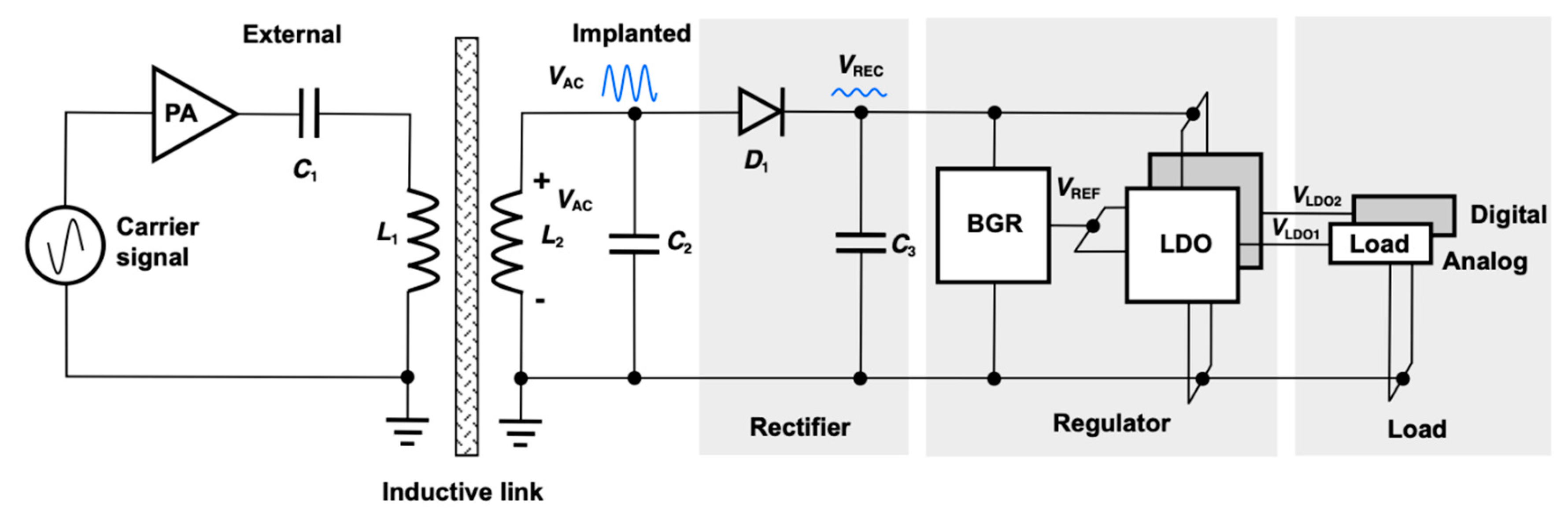
:1. Introduction
2. Architecture of the BGR Circuit
2.1. Conventional BGR Scheme
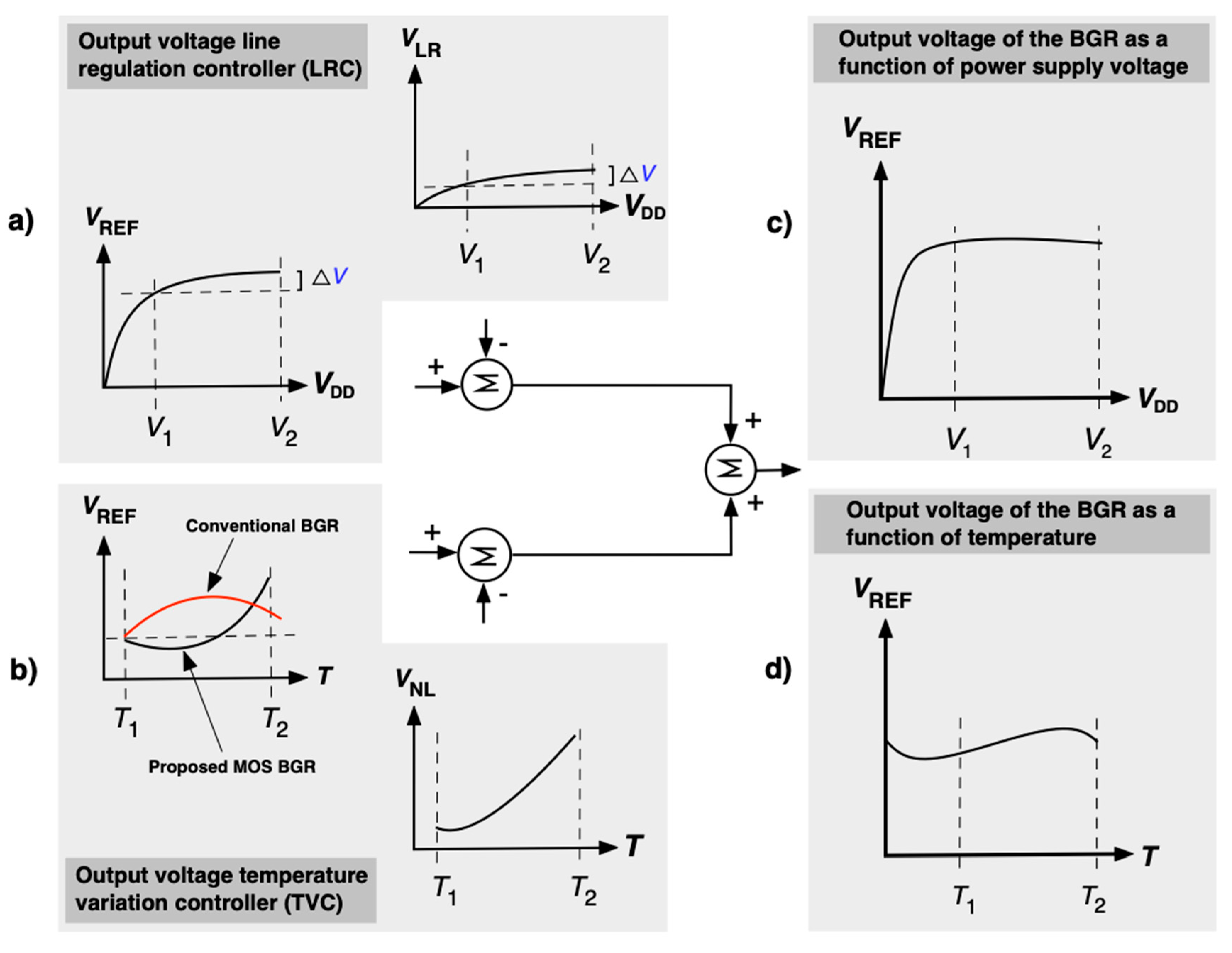
2.2. Proposed BGR
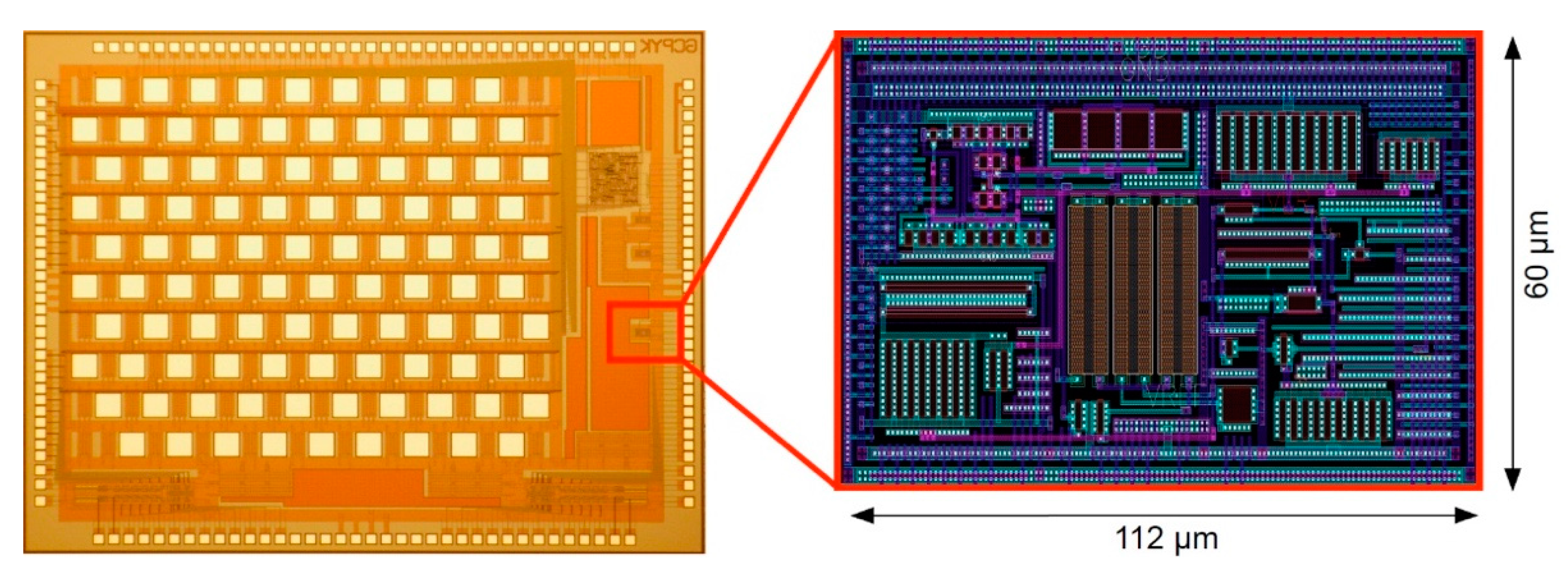
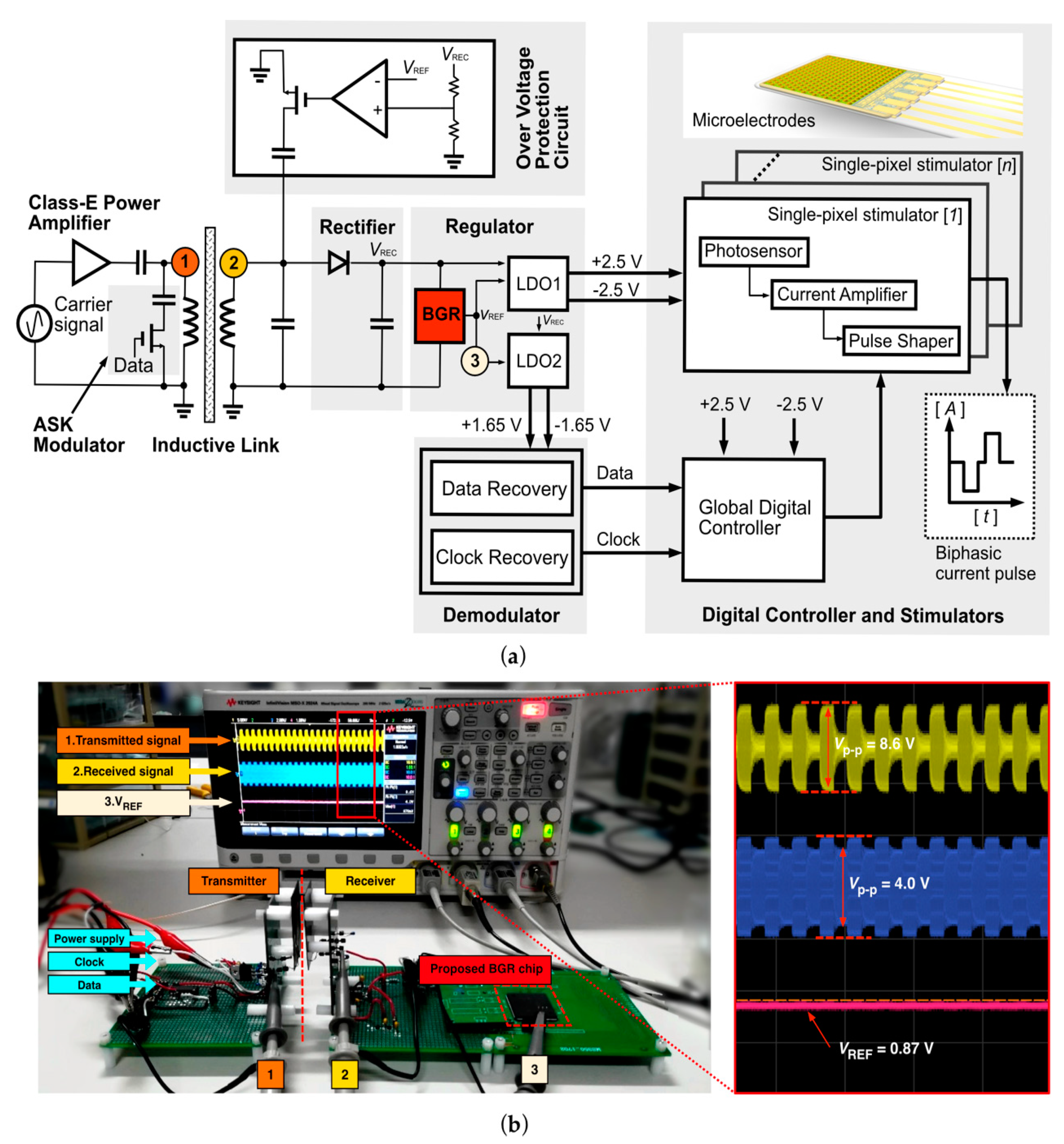
3. Simulation and Experimental Results
4. Conclusions
Author Contributions
Funding
Acknowledgments
Conflicts of Interest
Appendix A
Appendix B

References
- Ritter, R.; Handwerker, J.; Liu, T.; Ortmanns, M. Telemetry for Implantable Medical Devices: Part 1—Media Properties and Standards. IEEE Solid-State Circuits Mag. 2014, 6, 47–51. [Google Scholar] [CrossRef]
- Kang, H.; Abbasi, W.H.; Kim, S.; Kim, J. Fully Integrated Light-Sensing Stimulator Design for Subretinal Implants. Sensors 2019, 19, 536. [Google Scholar] [CrossRef] [PubMed] [Green Version]
- Tokuda, T.; Takeuchi, Y.; Sagawa, Y.; Noda, T.; Sasagawa, K.; Nishida, K.; Ohta, J. Development and in vivo Demonstration of CMOS-Based Multichip Retinal Stimulator with Simultaneous Multisite Stimulation Capability. IEEE Trans. Biomed. Circuits Syst. 2010, 4, 445–453. [Google Scholar] [CrossRef] [PubMed]
- Ayton, L.N.; Blamey, P.J.; Guymer, R.H.; Luu, C.D. First-in-Human Trial of a Novel Suprachoroidal Retinal Prosthesis. PLoS ONE 2014, 9, e115239. [Google Scholar] [CrossRef] [PubMed] [Green Version]
- Kofman, K.E.; Buckley, T.; McGrouther, D.A. Complications of transcutaneous metal devices. Eur. J. Plast. Surg. 2012, 35, 673–682. [Google Scholar] [CrossRef] [PubMed] [Green Version]
- Kuo, P.-H.; Wong, O.-Y.; Tzeng, C.-K.; Wu, P.-W.; Chiao, C.-C.; Chen, P.-H.; Chen, P.-C.; Tsai, Y.-C.; Chu, F.-L.; Ohta, J.; et al. Improved Charge Pump Design and Ex Vivo Experimental Validation of CMOS 256-Pixel Photovoltaic-Powered Subretinal Prosthetic Chip. IEEE Trans. Biomed. Eng. 2019, 67, 1490–1504. [Google Scholar] [CrossRef] [PubMed]
- Pixium Vision S A. 2001. Available online: http://pixium-vision.com (accessed on 1 April 2020).
- Lee, B.; Kiani, M.; Ghovanloo, M. A Triple-Loop Inductive Power Transmission System for Biomedical Applications. IEEE Trans. Biomed. Circuits Syst. 2016, 10, 138–148. [Google Scholar] [CrossRef] [PubMed]
- Jegadeesan, R.; Nag, S.; Agarwal, K.; Member, S. Enabling Wireless Powering and Telemetry for Peripheral Nerve Implants. IEEE J. Biomed. Health Inform. 2015, 19, 958–970. [Google Scholar] [CrossRef] [PubMed]
- Lo, Y.; Chen, K.; Gad, P.; Liu, W. An On-Chip Multi-Voltage Power Converter with Leakage Current Prevention Using 0.18 µm High-Voltage CMOS Process. IEEE Trans. Biomed. Circuits Syst. 2016, 10, 163–174. [Google Scholar] [CrossRef] [PubMed]
- Hu, Y.; Gervais, J.F.; Sawan, M. High power efficiency inductive link with full-duplex data communication. Proc. IEEE Int. Conf. Electron. Circuits Syst. 2002, 1, 359–362. [Google Scholar] [CrossRef]
- Ha, S.; Khraiche, M.L.; Akinin, A.; Jing, Y.; Damle, S.; Kuang, Y.; Bauchner, S.; Lo, Y.H.; Freeman, W.R.; Silva, G.A.; et al. Towards high-resolution retinal prostheses with direct optical addressing and inductive telemetry. J. Neural Eng. 2016, 13, 1–19. [Google Scholar] [CrossRef] [PubMed]
- Tzschoppe, C.; Jörges, U.; Richter, A.; Lindner, B.; Ellinger, F. Theory and Design of Advanced CMOS Current Mirrors. In Proceedings of the 2015 SBMO/IEEE MTT-S International Microwave and Optoelectronics Conference (IMOC), Porto de Galinhas, Brazil, 3–6 November 2015; pp. 1–5. [Google Scholar] [CrossRef]
- Kim, J.; Basham, E.; Pedrotti, K.D. Geometry-based optimization of radio-frequency coils for powering neuroprosthetic implants. Med. Biol. Eng. Comput. 2013, 51, 123–134. [Google Scholar] [CrossRef] [PubMed]
- Razavi, B. Design of Analog CMOS Integrated Circuit, 2nd ed.; McGraw-Hill Education: New York, NY, USA, 2017. [Google Scholar]
- Adeeb, M.A.; Islam, A.B.; Haider, M.R.; Tulip, F.S.; Ericson, M.N.; Islam, S.K. An inductive link-based wireless power transfer system for biomedical applications. Act. Passiv. Electron. Compon. 2012, 2012, 879294. [Google Scholar] [CrossRef]
- Osaki, Y.; Hirose, T.; Kuroki, N.; Numa, M. 1.2-V Supply, 100-nW, 1.09-V Bandgap and 0.7-V Supply, 52.5-nW, 0.55-V Sub-bandgap Reference Circuits for Nanowatt CMOS LSIs. IEEE J. Solid-State Circuits 2013, 48, 1530–1538. [Google Scholar] [CrossRef]
- Ma, B.; Yu, F. A Novel 1.2–V 4.5-ppm/°C Curvature-Compensated CMOS Bandgap Reference. IEEE Trans. Circuits Syst. I Regul. Pap. 2014, 61, 1026–1035. [Google Scholar] [CrossRef]
- Becker-Gomez, A.; Lakshmi Viswanathan, T.; Viswanathan, T.R. A Low-Supply-Voltage CMOS Sub-Bandgap Reference. IEEE Trans. Circuits Syst. II Express Briefs 2008, 55, 609–613. [Google Scholar] [CrossRef]
- Duan, Q.; Roh, J.; Member, S. A 1.2-V 4.2-ppm C High-Order Curvature- Compensated CMOS Bandgap Reference. IEEE Trans. Circuits Syst. I Regul. Pap. 2015, 62, 662–670. [Google Scholar] [CrossRef]
- Mattia, O.E.; Klimach, H.; Bampi, S. Resistorless BJT bias and curvature compensation circuit at 3.4 nW for CMOS bandgap voltage references. Electron. Lett. 2014, 50, 863–864. [Google Scholar] [CrossRef] [Green Version]
- Gray, P.; Meyer, R. Analysis and Design of Analog Integrated Circuits, 5th ed.; John Wiley and Sons: Hoboken, NJ, USA, 2010. [Google Scholar]
- Tsividis, Y.P.; Ulmer, R.W. A CMOS Voltage Reference. IEEE J. Solid-State Circuits 1978, 13, 774–778. [Google Scholar] [CrossRef]
- Pelgrom, M.J.M.; Duinmaijer, A.C.J.; Welbers, A.P.G. Matching properties of MOS transistors. IEEE J. Solid-State Circuits 1989, 24, 1433–1439. [Google Scholar] [CrossRef]


| Component | Parameter | Component | Parameter |
|---|---|---|---|
| MP1, MP2 | W = 10 µm, L = 5 µm | MN1, MN2, MN3 | W = 3.5 µm, L = 1 µm |
| MP3 | W = 20 µm, L = 1 µm | MN4 | W = 50 µm, L = 1 µm |
| MP4 | W = 2 µm, L = 5 µm | MN5 | W = 2 µm, L = 1 µm |
| MP5 | W = 50 µm, L = 1 µm | MN6 | W = 0.9 µm, L = 1 µm |
| MP6 | W = 5 µm, L = 1 µm | MN7 | W = 80 µm, L = 1 µm |
| MP7 | W = 1 µm, L = 25 µm | MN8 | W = 10 µm, L = 1 µm |
| MP8 | W = 25 µm, L = 1 µm | R1 | 40 kΩ |
| MP9 | W = 1 µm, L = 1.5 µm | R2 | 20 kΩ |
| Parameter | This Work | [18] | [19] |
|---|---|---|---|
| Technology | CMOS 0.35 µm | CMOS 0.18 µm | CMOS 0.18 µm |
| Supply voltage (V) | 3.3 | 1.2 | 1.4 |
| Line regulation | 1.85 mV/V (2.3–5 V) 0.4 mV/V (2.5–13 V) 1 | 0.054%/V (1.2–2) | ±0.3 mV (1.1–1.8) |
| PSRR (dB) | −54 | −84 | −75 |
| TC (ppm/°C) | 11.9 | 3.4 | 4 |
| Active area (mm2) | 0.0067 | 0.036 | - |
© 2020 by the authors. Licensee MDPI, Basel, Switzerland. This article is an open access article distributed under the terms and conditions of the Creative Commons Attribution (CC BY) license (http://creativecommons.org/licenses/by/4.0/).
Share and Cite
Zawawi, R.B.A.; Abbasi, W.H.; Kim, S.-H.; Choi, H.; Kim, J. Wide-Supply-Voltage-Range CMOS Bandgap Reference for In Vivo Wireless Power Telemetry. Energies 2020, 13, 2986. https://doi.org/10.3390/en13112986
Zawawi RBA, Abbasi WH, Kim S-H, Choi H, Kim J. Wide-Supply-Voltage-Range CMOS Bandgap Reference for In Vivo Wireless Power Telemetry. Energies. 2020; 13(11):2986. https://doi.org/10.3390/en13112986
Chicago/Turabian StyleZawawi, Ruhaifi Bin Abdullah, Wajahat H. Abbasi, Seung-Hwan Kim, Hojong Choi, and Jungsuk Kim. 2020. "Wide-Supply-Voltage-Range CMOS Bandgap Reference for In Vivo Wireless Power Telemetry" Energies 13, no. 11: 2986. https://doi.org/10.3390/en13112986