Article

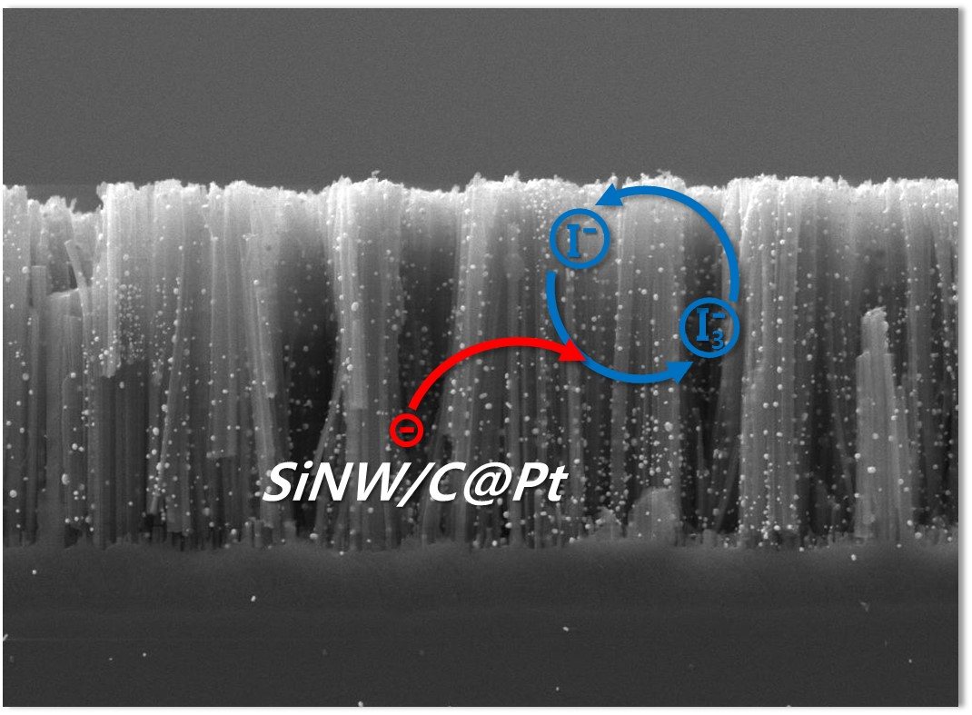
SiNW/C@Pt Arrays for High-Efficiency Counter Electrodes in Dye-Sensitized Solar Cells

1
Convergence Materials Research Center, Gumi Electronics and Information Technology Research Institute, Cheomdangieop 1-ro 17, Sandong-myeon, Gumi 39171, Korea
2
Graduate School of Energy and Environment (KU-KIST Green School), Korea University, 145, Anam-ro, Seongbuk-gu, Seoul 02841, Korea
3
Department of Materials Science and Engineering, Korea University, 145, Anam-ro, Seongbuk-gu, Seoul 02841, Korea
*
Authors to whom correspondence should be addressed.
Energies 2020, 13(1), 139; https://doi.org/10.3390/en13010139
Submission received: 27 November 2019 / Revised: 21 December 2019 / Accepted: 24 December 2019 / Published: 27 December 2019
(This article belongs to the Collection Advanced Materials for Energy Conversion and Storage Devices)

Abstract

:
Modern energy needs and the pressing issue of environmental sustainability have driven many research groups to focus on energy-generation devices made from novel nanomaterials. We have prepared platinum nanoparticle-decorated silicon nanowire/carbon core–shell nanomaterials (SiNW/C@Pt). The processing steps are relatively simple, including wet chemical etching to form the silicon nanowires (SiNWs), chemical vapor deposition to form the carbon shell, and drop-casting and thermal treatment to embed platinum nanoparticles (Pt NPs). This nanomaterial was then tested as the counter electrode (CE) in dye-sensitized solar cells (DSSCs). SiNW/C@Pt shows potential as a good electrocatalyst based on material characterization data from Raman spectroscopy and X-ray photoelectron spectroscopy (XPS). Raman spectroscopy shows that the surface reactivity of the SiNW/C is increased by the decoration of Pt NPs. These data also show that the carbon shell included both graphitic (sp 2 hybridization) and defective (sp 3 hybridization) phases of carbon. We achieved the minimum charge-transfer resistance of 0.025 · cm 2 and the maximum efficiency of 9.46% with a symmetric dummy cell and DSSC device fabricated from the SiNW/C@Pt CEs, respectively.

Graphical Abstract

1. Introduction

Nanowires have been studied extensively over the past decade due to their versatility and applications as promising building components in next-generation nanoscale devices like electrochemical batteries [1,2,3,4], biosensors [5,6,7], light-emitting diodes (LEDs) [8,9], transparent conducting electrodes [10], solar cells [11,12], and metamaterials [13,14]. Recent efforts have focused on improving the characteristics of such materials with core–shell nanowires. For example, Sanming et al. synthesized hierarchical NiCo 2 O 4 @NiWO 4 core–shell nanowire arrays and found that these perform excellently as supercapacitors [4]. Yao et al. synthesized N-doped Li 4 Ti 5 O 12 (N-LTO) with TiC/C skeletons for ultrafast Li ion storage. This material demonstrated outstanding rates and cycling stability [15].
Core–shell nanowires can also be used as electrocatalysts. Bai et al. synthesized Ag 2 S@MoS 2 core–shell nanowires with different loadings of MoS 2 to be used in producing hydrogen via photocatalysis. This material exhibited the highest H 2 production rate with a moderate loading of MoS 2 [16]. Likewise, the above-mentioned applications are good examples that nanowires’ key feature of a large surface area grants them the desired performance characteristics. In the present study, we fabricated silicon nanowire (SiNW) arrays using metal-assisted chemical etching (MaCE) for use as counter electrodes (CEs) in dye-sensitized solar cells (DSSCs). The large surface area of the SiNW makes it an effective electrocatalyst, but silicon on its own lacks electrocatalytic activity. Therefore, we used thermal chemical vapor deposition (CVD) to deposit a carbon shell on the surface of the SiNWs to improve electrocatalytic activity. The resultant carbon shell includes many defects, which encourage electrocatalysis.
In recent years, defective carbon nanomaterials with no heteroatom doping have been studied as electrocatalysts. The mechanism of this remains unclear, but we at least know that the edge of graphite is more active than the graphite’s basal plane [17]. Dai et al. prepared undoped and edge-rich graphene and showed its superior performance as an efficient metal-free electrocatalyst to encourage the oxygen reduction reaction (ORR) [18]. Hu et al. used undoped pure-carbon nanocages to address the influence of intrinsic carbon defects on ORR activity and found that their material performed better than materials prepared with heteroatoms such as B- or N-doped carbon [19].
Meanwhile, many research groups have applied nanocomposites with various metal nanoparticles (NPs) (Co [20], Pt [21], Rh [22], Au [23], Ni 2 P [24], and PdAg [25]) doped onto nanocarbon materials (carbon nanotubes (CNTs) or graphene oxide (GO)) as electrochemical catalysts to maximize the electrocatalytic activity of the material. Chen et al. synthesized Co@N-CNTs@r-GO to catalyze the hydrogen evolution reaction (HER). This material exhibited excellent electrocatalytic activity over a wide pH range, much better than most Co-based electrocatalysts [20]. Pan et al. also prepared Ni 2 P NPs on N-doped reduced graphene oxide (Ni 2 P/NRGO) via in situ thermal decomposition for catalyzing hydrogen evolution activity [24].
In this study, SiNW arrays were fabricated via MaCE to yield SiNWs with rough surfaces. Carbon shells were deposited along the surfaces of the SiNWs, consisting of both graphitic (sp 2 hybridization) and defective (sp 3 hybridization) carbon. According to Dai’s report, these defects act as electrocatalytically active sites [17]. Our material exploits the combination of the defective carbon shell supported by the SiNW array and Pt NPs decorated on the carbon shell (SiNW/C@Pt) to maximize the electrocatalytic activity that governs I 3 reduction in DSSCs. Our tests show that SiNW/C@Pt can be used as a CE because it exhibits the extremely low charge-transfer resistance (R c t ) of 0.025 · cm 2 in electrochemical impedance spectroscopy (EIS) measurements. We obtained a maximum efficiency of 9.46% in a DSSC device fabricated from SiNW/C@Pt.

2. Materials and Methods

2.1. Fabrication of SiNWs

SiNW arrays were fabricated using metal-assisted chemical etching (MaCE) [26]. A commercially available heavily doped n-type Si wafer with a resistivity of 0.001–0.003 · cm (Global Wafer) was cut into 1.5 × 1.5 cm 2 squares. These Si pieces were cleaned in ethanol, 2-propanol, and acetone, and were then subjected to ultraviolet-ozone (UVO) cleaning for 30 min. The clean Si pieces were then etched in a solution of 5 M HF and 0.002 M AgNO 3 . After 15–20 min, chemical etching was arrested by submerging the Si pieces in a water bath. Silver dendrites present on the surface of the Si pieces were then removed by placing the pieces in diluted HNO 3 for 20 min. Finally, the Si pieces were rinsed with deionized water and acetone and were subsequently dried by blowing N 2 gas over them.

2.2. Fabrication of SiNW/C@Pt

The carbon shell was deposited by thermal CVD on the SiNW surface. After raising the temperature of the reaction tube to 1050 ° C , 100 sccm of H 2 and 100 sccm of CH 4 were introduced simultaneously into the reaction tube for 5 min. Finally, the reaction was stopped quickly to prevent further growth of the carbon shell by air circulation quenching.
Next, Pt NPs were decorated on the SiNW surface using a simple drop-casting method. First, we prepared a Pt solution of 10 mM H 2 PtCl 6 in ethanol. SiNW/C pieces prepared as described above were treated with a UVO cleaner for 7 min to make their surfaces hydrophilic. The Pt solution was dropped onto the SiNW/C piece and allowed to dry naturally, followed by thermal treatment at 450 ° C for 30 min under an Ar atmosphere.

2.3. Fabrication of DSSCs

To prepare DSSCs, a fluorine-doped tin oxide substrate (FTO, Nippon Sheet Glass, Pilkington TEC) was cleaned sequentially with a detergent solution, deionized water, an ethanol/acetone mixture solution [1/1 (v/v)], and 2-propanol in ultrasonic baths for 40 min in total, followed by UVO treatment for 15 min. Nanocrystalline TiO 2 paste (20 nm, ENB-Korea) was coated with a doctor blade onto the cleaned FTO substrate, which was subsequently annealed at 500 ° C for 1 h. After annealing, the TiO 2 -coated FTO substrate was immersed for 12 h at 25 ° C in 0.3 mM (Bu 4 N) 2 [Ru(dcbpyH) 2 (NCS) 2 ] (termed N719) dye in a solution of acetonitrile and tert-butanol [1/1 (v/v)].

2.4. Characterization and Measurements

Samples of SiNW, SiNW/C, and SiNW/C@Pt were characterized using scanning electron microscopy (SEM, Hitachi S-4700, acceleration voltage: 5.0 kV), transmission electron microscopy (TEM, JEOL JEM-2100F), energy-dispersive X-ray fluorescence spectroscopy (EDX, Oxford Instrument), X-ray photoelectron spectroscopy (XPS, ULVAC-PHI X-TOOL), X-ray diffraction (XRD, Rigaku, SmartLab), and Raman spectroscopy (LabRam ARAMIS IR2), the last of which used a 532 nm diode laser. Current density–voltage (J–V) curves were measured using a solar simulator (ABET Technology, LS 150) under 100 mW/cm 2 and AM 1.5 G. Electrochemical impedance spectroscopy (EIS) and cyclic voltammograms (CVs) of the symmetric and full cells were recorded with a commercial electrochemical apparatus (Solartron Electrochemical Workstation).

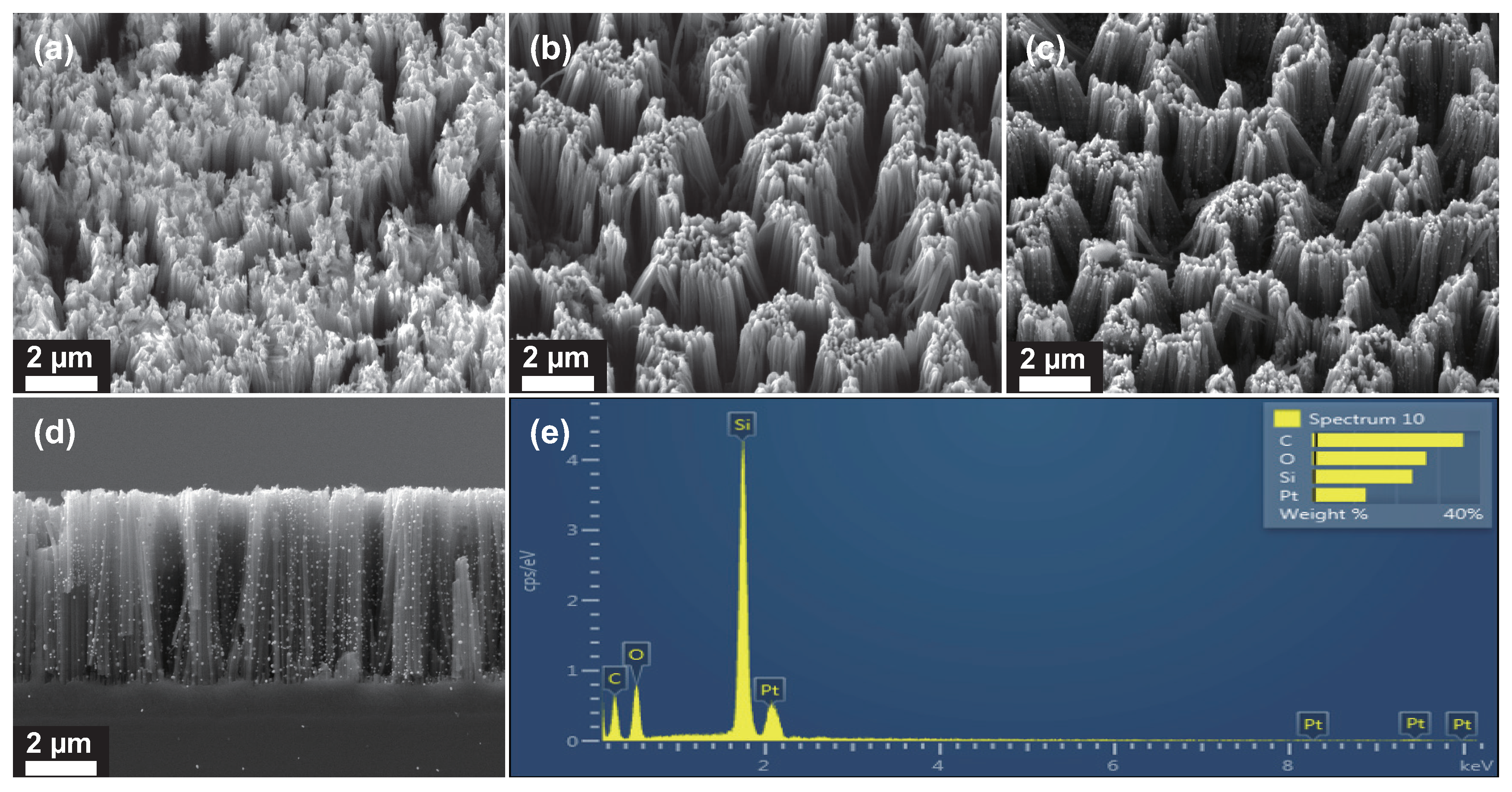
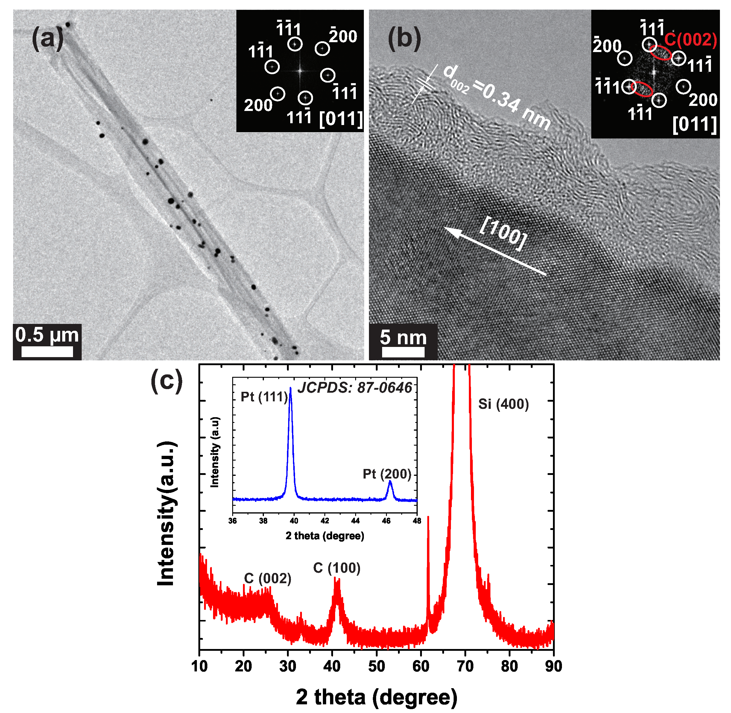
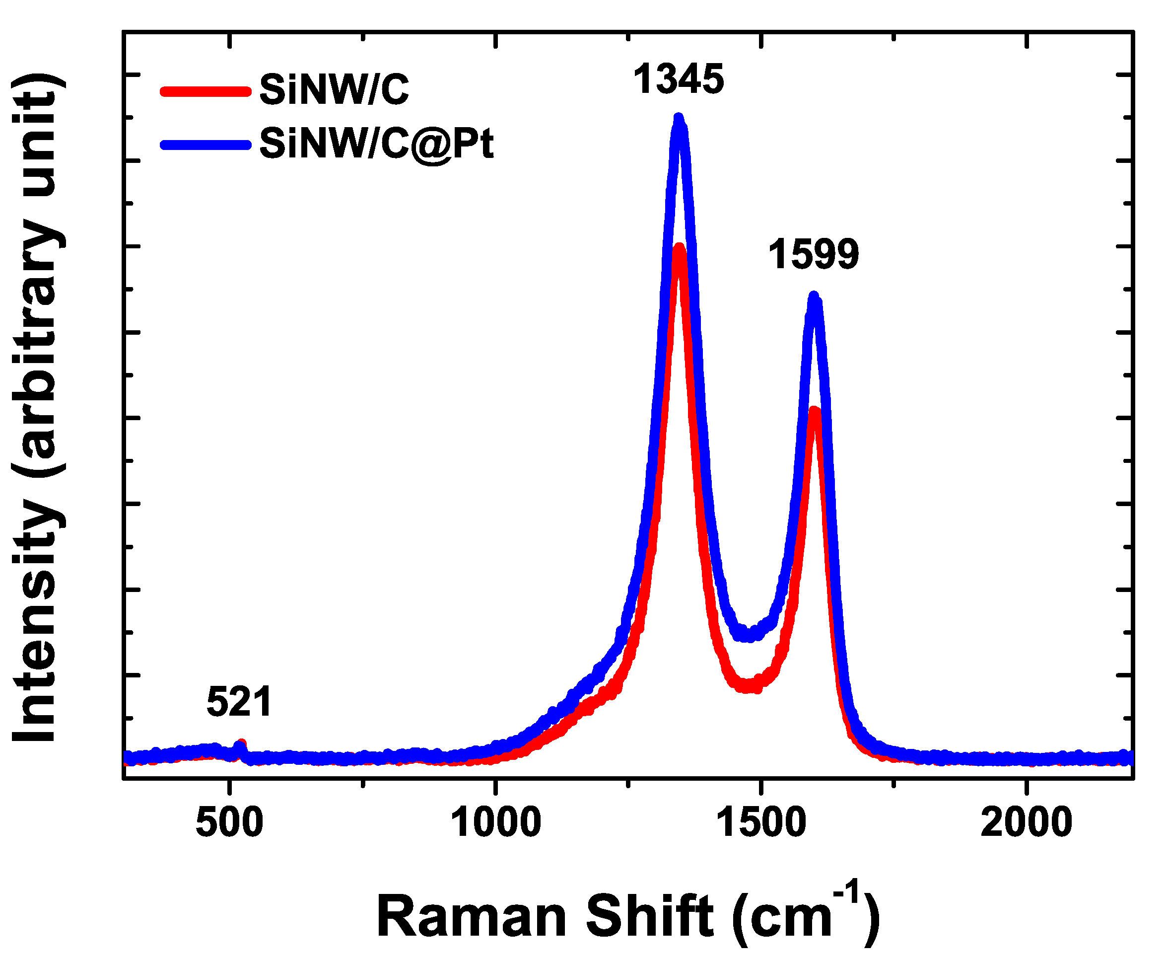
3. Results and Discussion

Figure 1 shows SEM images of the SiNW, SiNW/C, and SiNW/C@Pt samples and the elemental composition of the final SiNW/C@Pt material. SiNW arrays were formed on Si substrates using MaCE and had diameters ranging from 60 to 180 nm and lengths up to 5.4 μ m. In Figure 1a–c, one can see that the SiNW arrays are packed densely and bundled together because of mutual attraction [27,28]. The surface of the pristine SiNW with no carbon shell is sharp and coarse but becomes smooth after the carbon shell is deposited. Figure 1c,d shows the presence of Pt NPs decorated on the carbon shell. The elemental analysis in Figure 1e was obtained from the SiNW/C@Pt. The Si, C, Pt, and O in this plot come from the SiNW, carbon shell, Pt NPs, and oxides that form between the SiNW and the carbon shell.
Figure 2a,b presents a low-resolution TEM image of a single SiNW/C@Pt and a high-resolution TEM image of the SiNW/C with no Pt NPs, respectively. As shown in Figure 2b, the distance between Si (200) fringes, measured perpendicular to the wire axis in the [100] direction, is about 0.27 nm, which is almost identical to the same measurement of face-centered cubic (fcc) Si (JCPDS No. 80-0018). The fast Fourier-transformed electron diffraction (FFT-ED) pattern recorded from the [011] direction confirms that the SiNWs were formed from single-crystalline Si in the [100] direction. The carbon shells grown on the SiNW surface along the wire axis had an inter-distance of about 0.34 nm, and XRD patterns confirmed that the (002) plane peaked at 25.97 ° (see Figure 2c and the FFT-ED pattern in the inset of Figure 2b). We confirmed that the Pt NPs decorated on the material’s surface were successfully immobilized on the carbon shell using the images in Figure 1b and Figure 2a. The inset of Figure 2c shows an XRD pattern from the Pt NPs decorated on the carbon shell. The Pt NPs show two peaks at about 2 θ = 39.7 ° and 46.2 ° , which correspond to the (111) plane with the inter-planar spacing of 0.22 nm and the (200) plane with the inter-planar spacing of 0.20 nm, respectively. Therefore, the Pt NPs resemble face centered cubic (fcc) Pt (JCPDS No. 87-0646).
Figure 3 presents Raman spectra of the SiNW/C and SiNW/C@Pt samples. Three peaks are apparent. The peak at 521 cm 1 is caused by the scattering of the first-order transverse optical (TO) phonon in the Si substrate. The most distinct peaks in the Raman spectra are the G band appearing at 1599 cm 1 and the D band at 1345 cm 1 . The G band originates from the in-plane vibration of sp 2 -hybridized carbon atoms and has a doubly degenerate phonon mode with E 2 g symmetry at the center of the Brillouin zone [29], thus indicating the presence of graphitic carbon in the carbon shell. The D band is induced by the presence of defects and has the breathing mode of A 1 g symmetry [30]. Though the I D : I G ratios of both SiNW/C and SiNW/C@Pt were nearly 1.40, the Raman intensity increased after the Pt NPs were decorated on the SiNW/C, indicating that the Pt NPs encourage surface reactions. Therefore, we expect that SiNW/C@Pt will serve as a very efficient electrocatalyst.
We investigated the functional groups and chemical states present in the SiNW/C@Pt using XPS analysis, and the results are shown in Figure 4. The survey scan in Figure 4a shows peaks from Si 2p, Si 2s, C 1s, and Pt 4f; these indicate the presence of the carbon shell on the SiNW surface and the Pt NPs on the carbon shell. High-resolution XPS spectra corresponding to C 1s and Pt 4f from SiNW/C@Pt are shown in Figure 4b,c, respectively. In Figure 4b, the peak at 284.6 eV is usually attributed to the C–C bond (basal-plane sp 2 hybridization), and the peaks at 285.5 eV and 288.0 eV are typically assigned to the C–O and COOH functional groups (defect sp 3 hybridization), respectively. Finally, Figure 4c shows the XPS spectra of Pt 4f doublets (4f 7 / 2 and 4f 5 / 2 ) for the Pt NPs on top of the SiNW/C matrix. The principal doublets at 71.0 eV (Pt 4f 7 / 2 ) and 74.4 eV (Pt 4f 5 / 2 ) are characteristic of metallic Pt (Pt 0 ). The peaks at 72.0 eV (Pt 4f 7 / 2 ) and 75.3 eV (Pt 4f 5 / 2 ) correspond to Pt 2 + , and the peaks located at 76.3 eV and 77.9 eV correspond to Pt 4 + . The principal Pt 4f 7 / 2 and 4f 5 / 2 peaks were slightly shifted to binding energies lower than the commonly accepted binding energies of Pt 4f 7 / 2 and 4f 5 / 2 , perhaps due to electron transfer from the SiNW/C to the Pt NPs [31].
To test its catalytic performance, the SiNW/C@Pt material was used to fabricate several DSSCs. Since the base structure of the SiNW has high conductivity with its large surface area, SiNW/C@Pt should serve well as a counter electrode (CE) in DSSCs. Figure 5a shows the current density–voltage (J–V) characteristics of the DSSCs fabricated from a reference material (FTO/Pt), SiNW/C, and SiNW/C@Pt. The photovoltaic performance of these DSSCs is summarized in Table 1. The reference device exhibited an efficiency of 8.08% with 14.41 mA/cm 2 , 0.789 V, and 71.06% as J s c , V o c , and FF, respectively. When this reference CE was replaced with a SiNW/C CE, the efficiency (7.92%) was quite comparable and the photovoltaic parameters were J s c of 14.30 mA/cm 2 , V o c of 0.789 V, and FF of 70.19%. The greatest efficiency was obtained when Pt NPs were decorated on the surface of the SiNW/C. The DSSC made from SiNW/C@Pt showed η of 9.46% with J s c of 15.95 mA/cm 2 , V o c of 0.797 V, and FF of 74.41%. The main factor that increases the efficiency is the current density in the DSSC. Electrocatalytic activity and cyclic voltammograms were used to measure this feature of the DSSC.
CV measurements were taken from symmetrical dummy cells at a scan rate of 100 mV·s 1 to eliminate the influence of photoanodes. The electrolyte was sandwiched between identical CEs. The equivalent circuit for the analysis and the CV curves measured in the potential range of −1.0 to 1.0 V are shown in Figure 5b,c, respectively. The electrocatalytic activity of the CEs can be deduced from the slopes and current density of these CV curves. As observed in Figure 5c, the slope of the SiNW/C@Pt in the low-potential range is steeper than the others and the current density in the high-potential range is greater, which indicates that the SiNW/C@Pt offers superior electrocatalytic activity that encourages the I /I 3 redox reaction.
The internal resistances and electrocatalytic activity of CEs significantly influence photovoltaic efficiency, so electrochemical impedance spectroscopy (EIS) measurements were carried out with symmetrical dummy cells to evaluate the electrocatalytic activity of SiNW/C@Pt. Figure 5d illustrates Nyquist plots of the reference cell, SiNW/C, and SiNW/C@Pt, in which the high-frequency intercept yields the series resistance (R s ) and the diameter of the first semicircle at high frequencies represents the charge-transfer resistance (R c t ) at the interface between the electrolyte and the electrode surface. According to these calculated resistances, we learned that the R s value of SiNW/C@Pt is 5.01 · cm 2 , which is similar to the R s value of the reference cell (5.75 · cm 2 ) and that of SiNW/C (5.10 · cm 2 ), whereas the R c t has the significantly lower value of 0.025 · cm 2 . Obviously, the scattered Pt NPs decorated on the carbon shell are responsible for the relatively low value of R c t .

4. Conclusions

This study demonstrated methods for the preparation and photovoltaic application of a novel nanomaterial, a silicon nanowire/carbon core–shell nanomaterial with platinum nanoparticles (SiNW/C@Pt). First, SiNW arrays were prepared by metal-assisted chemical etching (MaCE), and then a carbon shell was deposited on these; finally drop-casting and thermal treatment were used to decorate Pt NPs. The tests reported above show that SiNW/C@Pt performs well as the counter electrode (CE) in DSSC devices. The SiNW/C@Pt CE exhibited extremely low charge-transfer resistance (0.025 · cm 2 ) and a high efficiency of 9.46%. This material serves as an efficient electrocatalyst because it combines three mechanisms that encourage electrocatalysis: the electronic defects in the carbon shell, the high surface area of the SiNW arrays, and the efficient electrocatalytic activity of Pt nanoparticles. Our results suggest that nanomaterials that combine defective carbon and nanoparticles can serve as highly efficient electrocatalysts in photovoltaic devices.

Author Contributions

Conceptualization, J.K. and Y.J.; methodology, J.K., S.M.K., and C.L.; formal analysis, J.K. and H.-J.K.; investigation, J.K. and S.J.; resources, D.K. and Y.J; data curation, J.K.; writing–original draft preparation, J.K. and Y.J.; writing–review and editing, S.-M.K., D.K., and Y.J.; visualization, J.K. and S.J.; supervision, Y.K.; funding acquisition, S.-M.K. and Y.J. All authors have read and agreed to the published version of the manuscript.

Funding

This research was supported by the Technology Development Program to Solve Climate Changes of the National Research Foundation (NRF) funded by the Ministry of Science, ICT & Future Planning (NRF-2017M1A2A2087325) and by MOTIE/KIAT (No. N0002431).

Conflicts of Interest

The authors declare no conflict of interest.

Abbreviations

The following abbreviations are used in this manuscript:
DSSCsDye-sensitized solar cells
CEsCounter electrodes
ORROxygen reduction reaction
SiNWsSilicon nanowire arrays
MaCEMetal-assisted chemical etching
NPsNanoparticles
SEMScanning electron microscopy
TEMTransmission electron microscopy
EDXEnergy-dispersive X-ray fluorescence spectroscopy
XPSX-ray Photoelectron spectroscopy
XRDX-ray diffraction
EISElectrochemical impedance spectroscopy
CVCyclic voltammogram
FTOFluorine-doped tin oxide

References

  1. Xia, X.; Tu, J.; Zhang, Y.; Wang, X.; Gu, C.; Zhao, X.B.; Fan, H.J. High-Quality Metal Oxide Core/Shell Nanowire Arrays on Conductive Substrates for Electrochemical Energy Storage. ACS Nano 2012, 6, 5531–5538. [Google Scholar] [CrossRef] [PubMed]
  2. Lu, X.F.; Chen, X.Y.; Zhou, W.; Tong, Y.X.; Li, G.R. α-Fe2O3@PANI Core–Shell Nanowire Arrays as Negative Electrodes for Asymmetric Supercapacitors. ACS Appl. Mater. Interfaces 2015, 7, 14843–14850. [Google Scholar]
  3. Wang, C.; Wu, L.; Wang, H.; Zuo, W.; Li, Y.; Liu, J. Fabrication and Shell Optimization of Synergistic TiO2-MoO3 Core–Shell Nanowire Array Anode for High Energy and Power Density Lithium-Ion Batteries. Adv. Func. Mater. 2015, 25, 3524–3533. [Google Scholar] [CrossRef]
  4. Chen, S.; Yang, G.; Jia, Y.; Zheng, H. Three-dimensional NiCo2O4@NiWO4 core–shell nanowire arrays for high performance supercapacitors. J. Mater. Chem. A 2017, 5, 1028–1034. [Google Scholar] [CrossRef]
  5. Chen, S.; Xie, Y.; De, A.; Berg, A.; Carlen, E.T. Electrical shielding for siliconnanowire biosensor in microchannels. Appl. Phys. Lett. 2013, 103, 173702. [Google Scholar] [CrossRef] [Green Version]
  6. Zhang, G.-J.; Chua, J.-H.; Chee, R.E.; Agarwal, A.; Wong, S.-M. Label-free direct detection of MiRNAs with silicon nanowire biosensors. Biosens. Bioelectron. 2009, 24, 2504–2508. [Google Scholar] [CrossRef]
  7. Duan, X.; Li, Y.; Rajan, N.K.; Routenberg, D.A.; Modis, Y.; Reed, M.A. Quantification of the affinities and kinetics of protein interactions using silicon nanowire biosensors. Nat. Nanotechnol. 2012, 7, 401–407. [Google Scholar] [CrossRef]
  8. Chen, C.-Y.; Zhu, G.; Hu, Y.; Yu, J.-W.; Song, J.; Cheng, K.-Y.; Peng, L.-H.; Chou, L.-J.; Wang, Z.L. Gallium Nitride Nanowire BasedNanogenerators and Light-Emitting Diodes. ACS Nano 2012, 6, 5687–5692. [Google Scholar] [CrossRef]
  9. Zimmler, M.A.; Voss, T.; Ronning, C.; Capasso, F. Exciton-related electroluminescence from ZnO nanowire light-emitting diodes. Appl. Phys. Lett. 2009, 94, 241120. [Google Scholar] [CrossRef]
  10. Ahn, Y.; Jeong, Y.; Lee, D.; Lee, Y. Copper Nanowire–Graphene Core–Shell Nanostructure for Highly Stable Transparent Conducting Electrodes. ACS Nano 2015, 9, 3125–3133. [Google Scholar] [CrossRef]
  11. Fang, X.; Li, Y.; Wang, X.; Ding, J.; Yuan, N. Ultrathin interdigitated back-contacted silicon solar cell with light-trapping structures of Si nanowire arrays. Sol. Energy 2015, 116, 100–107. [Google Scholar] [CrossRef]
  12. Kim, H.T.; Lee, K.; Jin, W.; Um, H.D.; Lee, M.; Hwang, E.; Kwon, T.H.; Seo, K. Phosphorescent Energy Downshifting for Diminishing Surface Recombination in Silicon Nanowire Solar Cells. Sci. Rep. 2018, 8, 16974–16982. [Google Scholar] [CrossRef] [PubMed]
  13. Karvounis, A.; Gholipour, B.; MacDonald, K.F.; Zheludev, N.I. Giant Electro-Optical Effect through Electrostriction in a Nanomechanical Metalmaterial. Adv. Mater. 2019, 31, 1804801. [Google Scholar] [CrossRef] [PubMed] [Green Version]
  14. Karvounis, A.; Aspiotis, N.; Zeimpekis, I.; Ou, J.-Y.; Huang, C.-C.; Hewak, D.; Zheludev, N.I. Mechanochromic Reconfigurable Metasurfaces. Adv. Sci. 2019, 6, 1900974. [Google Scholar] [CrossRef]
  15. Yao, Z.; Xia, X.; Xie, D.; Wang, Y.; Zhou, C.; Liu, S.; Deng, S.; Wang, X.; Tu, J. Enhancing Ultrafast Lithium Ion Storage of Li4Ti5O12 by Tailored TiC/C Core/Shell Skeleton Plus Nitrogen Doping. Adv. Func. Mater. 2018, 28, 1802756. [Google Scholar] [CrossRef]
  16. Bai, L.; Cai, X.; Lu, J.; Li, L.; Zhong, S.; Wu, L.; Gong, P.; Chen, J.; Bai, S. Surface and Interface Engineering in Ag2S@MoS2 Core–Shell Nanowire Heterojunctions for Enhanced Visible Photocatalytic Hydrogen Production. ChemCatChem 2018, 10, 2107–2114. [Google Scholar] [CrossRef]
  17. Shen, A.; Zou, Y.; Wang, Q.; Dryfe, R.A.W.; Huang, X.; Dou, S.; Dai, L.; Wang, S. Oxygen Reduction Reaction in a Droplet on Graphite: Direct Evidence that the Edge Is More Active than the Basal Plane. Angew. Chem. Int. Ed. 2014, 53, 10804–10808. [Google Scholar] [CrossRef]
  18. Tao, L.; Wang, Q.; Dou, S.; Ma, Z.; Huo, J.; Wang, S.; Dai, L. Edge-rich and dopant-free graphene as a highly efficient metal-free electrocatalyst for the oxygen reduction reaction. Chem. Commun. 2016, 52, 2764–2767. [Google Scholar] [CrossRef]
  19. Jiang, Y.; Yang, L.; Sun, T.; Zhao, J.; Lyu, Z.; Zhuo, O.; Wang, X.; Wu, Q.; Ma, J.; Hu, Z. Significant Contribution of Intrinsic Carbon Defects to Oxygen Reduction Activity. ACS Catal. 2015, 5, 6707–6712. [Google Scholar] [CrossRef] [Green Version]
  20. Chen, Z.; Wu, R.; Liu, Y.; Guo, Y.; Sun, D.; Liu, M.; Fang, F. Ultrafine Co Nanoparticles Encapsulated in Carbon-Nanotubes-Grafted Graphene Sheets as Advanced Electrocatalysts for the Hydrogen Evolution Reaction. Adv. Mater. 2018, 30, 1802011. [Google Scholar] [CrossRef]
  21. Wan, T.-H.; Chiu, Y.-F.; Chen, C.-W.; Hsu, C.-C.; Cheng, I.-C.; Chen, J.-Z. Atmospheric-Pressure Plasma Jet Processed Pt-Decorated Reduced Graphene Oxides for Counter-Electrodes of Dye-Sensitized Solar Cells. Coatings 2016, 6, 44. [Google Scholar] [CrossRef]
  22. Wang, C.; Ciganda, R.; Yate, L.; Tuninetti, J.; Shalabaeva, V.; Salmon, L.; Moya, S.; Ruiz, J.; Astruc, D. Redox synthesis and high catalytic efficiency of transition-metal nanoparticle–graphene oxide nanocomposites. J. Mater. Chem. A 2017, 5, 21947–21954. [Google Scholar] [CrossRef]
  23. Govindhan, M.; Chen, A. Simultaneous synthesis of gold nanoparticle/graphene nanocomposite for enhanced oxygen reduction reaction. J. Power Sources 2015, 274, 928–936. [Google Scholar] [CrossRef]
  24. Pan, Y.; Chen, Y.; Lin, Y.; Li, Y.; Liu, Y.; Liu, C. Nickel phosphide nanoparticles-nitrogen-doped graphene hybrid as an efficient catalyst for enhanced hydrogen evolution activity. J. Power Sources 2015, 297, 45–52. [Google Scholar] [CrossRef]
  25. Song, F.-Z.; Zhu, Q.-L.; Yang, X.; Zhan, W.-W.; Pachfule, P.; Tsumori, N.; Xu, Q. Metal-Organic Framework Templated Porous Carbon-Metal Oxide/Reduced Graphene Oxide as Superior Support of Bimetallic Nanoparticles for Efficient Hydrogen Generation from Formic Acid. Adv. Energy Mater. 2018, 8, 170146. [Google Scholar] [CrossRef]
  26. Chen, C.-Y.; Wu, C.-S.; Chou, C.-J.; Yen, T.-J. Morphological Control of Single-Crystalline Silicon Nanowire Arrays near Room Temperature. Adv. Mater. 2008, 20, 3811–3815. [Google Scholar] [CrossRef]
  27. Zhang, M.-L.; Peng, K.-Q.; Fan, X.; Jie, J.-S.; Zhang, R.-Q.; Lee, S.-T.; Wong, N.-B. Preparation of Large-Area Uniform Silicon Nanowires Arrays through Metal-Assisted Chemical Etching. J. Phys. Chem. C 2008, 112, 4444–4450. [Google Scholar] [CrossRef]
  28. Togonal, A.S.; He, L.; Roca, I.C.; Rusli. Effect of Wettability on the Agglomeration of Silicon Nanowire Arrays Fabricated by Metal-Assisted Chemical Etching. Langmuir 2014, 30, 10290–10298. [Google Scholar] [CrossRef]
  29. Ferrari, A.C.; Robertson, J. Interpretation of Raman spectra of disordered and amorphous carbon. Phys. Rev. B 2000, 61, 14095. [Google Scholar] [CrossRef] [Green Version]
  30. Pimenta, M.A.; Dresselhaus, G.; Dresselhaus, M.S.; Cançado, L.G.; Jorio, A.; Saito, R. Studying disorder in graphite-based systems by Raman spectroscopy. Phys. Chem. Chem. Phys. 2007, 9, 1276–1291. [Google Scholar] [CrossRef]
  31. Cho, S.H.; Yang, H.N.; Lee, D.C.; Park, S.H.; Kim, W.J. Electrochemical properties of Pt/graphene intercalated by carbon black and its application in polymer electrolyte membrane fuel cell. J. Power Sources 2013, 225, 200–206. [Google Scholar] [CrossRef]
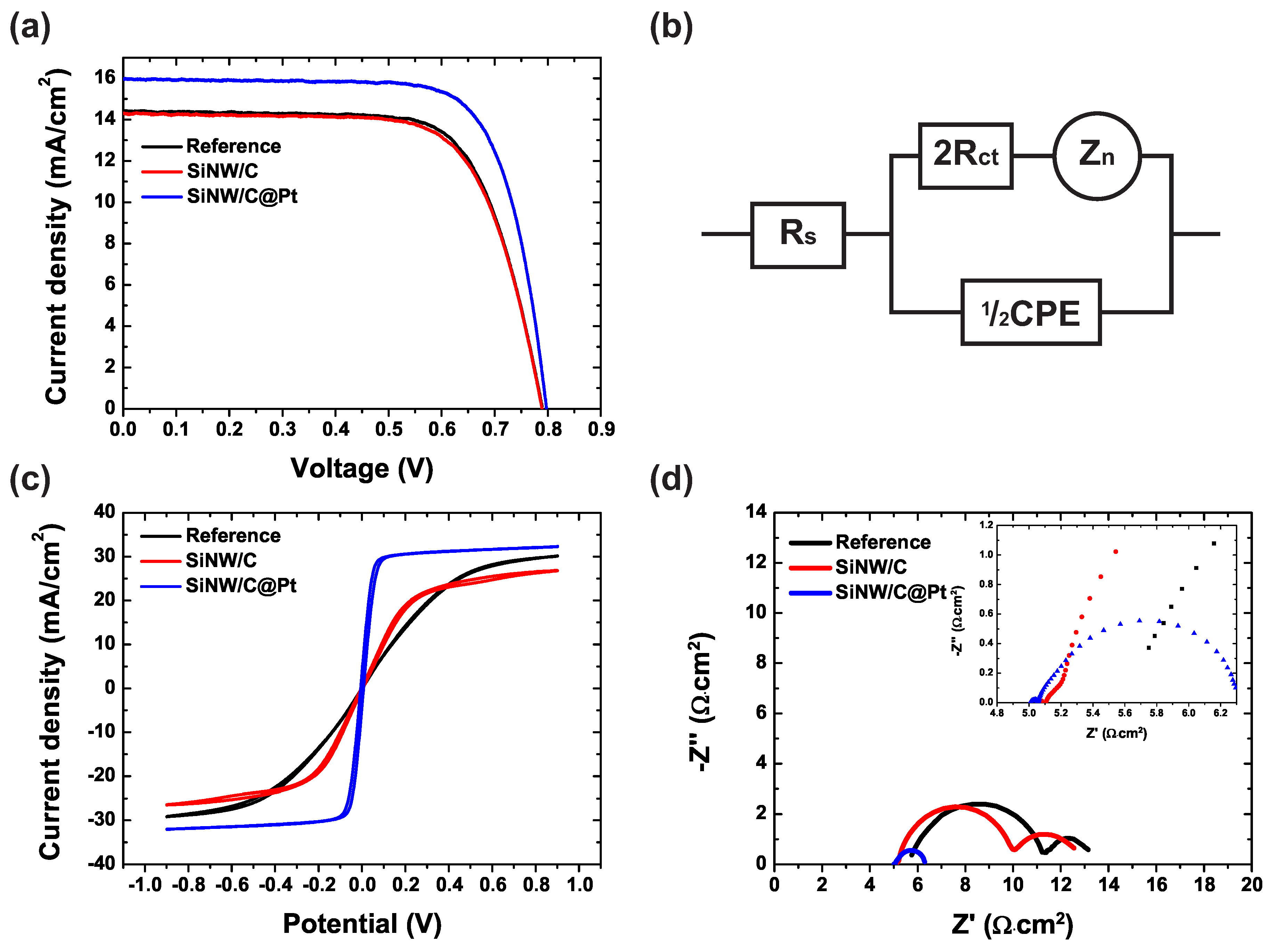
Figure 1. Scanning electron microscope images of (a) tilted silicon nanowire (SiNW); (b) tilted SiNW/C; (c) tilted and (d) cross-sectional SiNW/C@Pt; and (e) elemental analysis of SiNW/C@Pt.
Energies 13 00139 g001
Figure 2. (a) Low-resolution transmission electron microscopy image of SiNW/C@Pt (inset: fast Fourier-transformed electron diffraction (FFT-ED) pattern of platinum nanoparticles, Pt NPs); (b) high-resolution image of SiNW/C with no Pt NPs (inset: FFT-ED pattern of SiNW/C); and (c) XRD pattern of SiNW/C (inset: XRD pattern of Pt NPs).
Energies 13 00139 g002
Figure 3. Raman spectra of SiNW/C and SiNW/C@Pt.
Energies 13 00139 g003
Figure 4. X-ray photoelectron spectroscopy analysis of SiNW/C@Pt: (a) survey scan; (b) high-resolution spectrum of C 1s; and (c) high-resolution spectrum of Pt 4f.
Energies 13 00139 g004
Figure 5. (a) Current–voltage (J–V) characteristics of the dye-sensitized solar cells (DSSCs) fabricated with reference (fluorine-doped tin oxide (FTO)/Pt), SiNW/C, and SiNW/C@Pt counter electrodes measured under 1 sun illumination (AM 1.5 G, 100 mW/cm 2 ); (b) equivalent circuit model of the symmetrical dummy cells consisting of the identical counter electrodes (CEs); (c) cyclic voltammograms; and (d) Nyquist plots of the symmetrical dummy cells.
Energies 13 00139 g005
Table 1. Photovoltaic performance of the DSSCs fabricated with FTO/Pt, SiNW/C, and SiNW/C@Pt counter electrodes.
CounterJ sc V oc FF η R s R c t
Electrode(mA/cm 2 )(V)(%)(%)( · cm 2 )( · cm 2 )
Reference14.41 ± 0.20.789 ± 0.00271.06 ± 0.38.08 ± 0.175.752.725
SiNW/C14.30 ± 0.20.789 ± 0.00470.19 ± 0.57.92 ± 0.215.102.448
SiNW/C@Pt15.95 ± 0.10.797 ± 0.00274.41 ± 0.49.46 ± 0.135.010.025

