Article

Enhancing the Performance of Textured Silicon Solar Cells by Combining Up-Conversion with Plasmonic Scattering

1
Department of Electro-Optical Engineering, National Taipei University of Technology, No. 1, Section 3, Zhongxial East Road, Taipei 10608, Taiwan
2
Graduate Institute of Photonics and Optoelectronics, National Taiwan University, No. 1, Section 4, Roosevelt Road, Taipei 10617, Taiwan
*
Author to whom correspondence should be addressed.
Energies 2019, 12(21), 4119; https://doi.org/10.3390/en12214119
Submission received: 30 September 2019 / Revised: 21 October 2019 / Accepted: 28 October 2019 / Published: 28 October 2019
(This article belongs to the Special Issue Selected Papers from TIKI IEEE ICASI 2019)

Abstract

:
This paper experimentally demonstrates the benefits of combining an up-conversion (UC) layer containing Yb/Er-doped yttrium oxide-based phosphors with a plasmonic scattering layer containing indium nanoparticles (In-NPs) in enhancing the photovoltaic performance of textured silicon solar cells. The optical emissions of the Yb/Er-doped phosphors were characterized using photoluminescence measurements obtained at room temperature. Optical microscope images and photo current-voltage curves were used to characterize the UC emissions of Yb/Er-doped phosphors under illumination from a laser diode with a wavelength of 1550 nm. The plasmonic effects of In NPs were assessed in terms of absorbance and Raman scattering. The performance of the textured solar cells was evaluated in terms of optical reflectance, external quantum efficiency, and photovoltaic performance. The analysis was performed on cells with and without a UC layer containing Yb/Er-doped yttrium oxide-based phosphors of various concentrations. The analysis was also performed on cells with a UC layer in conjunction with a plasmonic scattering layer. The absolute conversion efficiency of the textured silicon solar cell with a combination of up-conversion and plasmonic-scattering layers (15.43%) exceeded that of the cell with an up-conversion layer only (14.94%) and that of the reference cell (14.45%).

Graphical Abstract

1. Introduction

Wafer-based crystalline silicon is currently the dominant photovoltaic technology. Lowering the price of electricity generated by photovoltaic systems will require improvements in conversion efficiency and reductions in manufacturing costs. A variety of light trapping techniques have been developed to reduce the reflectance of silicon solar cells and extend broadband performance. These methods include the creation of surface structures at the nano- and micro-scale [1,2,3,4,5], and taking advantage of the plasmonic effects of noble metal nanoparticles (NPs) [6,7,8]. Metallic nanoparticles exhibit strong optical extinction, due to the collective oscillation of free electrons, referred to as localized surface plasmon resonance (LSPR) [9,10]. The resonance wavelength is sensitive to the size and shape of the NPs as well as the surrounding material [11]. Nanoparticles of gold (Au NPs) [12,13,14], silver (Ag NPs) [15,16,17,18,19], and aluminum (Al NPs) [20,21,22] are widely used to induce light scattering, with the aim of trapping more of the light energy in order to create solar cells of greater efficiency. The maximum theoretical efficiency of a single-junction (single bandgap) crystalline silicon solar cell is approximately 31% under one sun AM 1.5G illumination [23,24]. There are two factors that greatly hinder the efficiency of single bandgap solar cells: 1) an inability to absorb photons with energy below the bandgap (long-wavelength photons), and 2) and the thermalization of photon energy above the bandgap (short-wavelength photons). Numerous methods have been developed to enhance conversion efficiency at short wavelengths, including the deposition of a down-conversion (DC) layer or a luminescence down-shift (LDS) layer on the front side of photovoltaic devices [25,26,27,28]. Up-conversion (UC) is another promising approach to recruiting sub-bandgap photons for solar cells (SCs) [29,30,31,32,33,34,35]. The photons emitted by UC phosphors carry more energy than do the photons excited in UC materials. This allows the conversion of infrared (IR) or near-IR (NIR) excitation into visible wavelengths. The fact that low energy photons (IR or NIR) are transmitted through silicon solar cells means that an up-conversion layer could be placed on the back-side of silicon solar cells. However, there has been relatively little research on the use of up-conversion in conjunction with plasmonic scattering to enhance the efficiency of silicon solar cells.
In previous studies, we used the broadband plasmonic forward-scattering of indium nanoparticles on textured silicon solar cells [36,37,38], or a NIR up-conversion layer on planar silicon solar cells [38], to enhance cell’s photovoltaic performance. In the current study, we deposited an up-conversion layer on the rear surface of textured silicon solar cells as well as a plasmonic scattering layer on the front surface. We found that by reducing reflectance, a layer of indium nanoparticles on the front surface of the solar cells allowed the penetration of a larger number of long-wavelength incident photons to excite phosphor particles on the rear surface, thereby enhancing UC efficiency. We first evaluated the UC performance of the up-conversion layer using photoluminescence (PL) measurements at room temperature. Optical reflectance, external quantum efficiency (EQE), and photovoltaic current density-voltage (J-V) characteristics were also used to assess the plasmonic effects of indium nanoparticles (In NPs) and the NIR up-conversion efficiency of YF3:Yb3+/Er3+ phosphors. Photovoltaic J-V measurements were then used to evaluate the performance of textured silicon solar cells with an up-conversion layer of SiO2 containing YF3:Yb3+/Er3+ phosphors of various concentrations (10 wt%, 20 wt%, 30 wt%) in conjunction with a plasmonic-scattering layer of In NPs (3 nm, 5 nm, 7 nm) in terms of short-circuit current-density (JSC) and conversion efficiency (η). Our results demonstrate the benefits of using an up-conversion layer in conjunction with a plasmonic-scattering layer to enhance the photovoltaic performance of textured silicon solar cells.

2. Materials and Methods

2.1. Preparation and Characterization of Up-Conversion and Plasmonic Scattering Layers

2.1.1. Up-Conversion Layer Comprising Yb/Er-Doped Yttrium Oxide-Based Phosphors

Before depositing an up-conversion layer, the silicon substrates (1 × 1 cm2) were subjected to ultrasonic cleaning using acetone (ACE) and isopropanol (IPA) and then rinsed in deionized (DI) water for 10 min and dried using high purity nitrogen gas. Three silicon substrates were respectively coated with an SOG (SiO2) layer containing Yb/Er-doped phosphors (YF3:Yb3+/Er3+) at concentrations of 10, 20, or 30 wt%. We fabricated a control sample in which the same substrate was coated with the same SOG layer but without phosphors. The deposition solution comprised 1.94 g of silicate solution (Emulsitone Company product, Whippany, NJ, USA) mixed with Yb/Er-doped yttrium oxide-based phosphors (New Prismatic Enterprise Company product, New Taipei City, Taiwan) at concentrations of 10, 20, and 30 wt%. The mixture was dropped onto the cleaned silicon substrates, where it remained for 12 s before undergoing spin-coating at 1500 rpm for 60 s. The coated samples were subsequently baked at 180 °C for 10 min on a hot-plate under an air atmosphere. Figure 1a presents a test sample with an up-conversion layer. We examined the surface morphology, chemical composition, and fluorescence emission of samples with an SOG layer containing Yb/Er-doped phosphors using scanning electron microscopy (SEM, Hitachi S-4700, Hitachi High-Tech Fielding Corporation, Tokyo, Japan), energy-dispersive X-ray spectroscopy (EDS, Hitachi S-4700, Hitachi High-Tech Fielding Corporation, Tokyo, Japan), and photoluminescence spectroscopy (PL, Ramboss 500i Micro-PL Spectroscopy, DONGWOO Optron, Korea).

2.1.2. Plasmonic Scattering Layer of SiO2 with Indium Nanoparticles

Quartz substrates were used as a template to characterize the plasmonic effects of indium nanoparticles in the UV-VIS band, due to their low absorption at those wavelengths. The substrates were subjected to ultrasonic cleaning in ACE and IPA before being rinsed in DI water for 10 min and dried under nitrogen flow. Films of indium were deposited at various depths (3 nm, 5 nm, and 7 nm) on the cleaned substrates using e-beam evaporation. Subsequent annealing in an RTA chamber at 200 °C for 20 min under H2 caused the indium films to transform into nano-sized indium particles. We then applied a 94 nm-thick SiO2 capping layer over the In NPs layer. Figure 1b presents a completed sample with a layer of SiO2 with embedded In NPs. The plasmonic effects of the In NPs were examined in terms of absorbance and Raman scattering measurements. The absorption spectra were corrected using a spectrometer (USB4000-VIS-NIR, Ocean Optics, Inc., FL, USA) with tungsten light source and reflective integrating sphere. Raman scattering spectra were corrected using a Raman spectrometer (UniRAM, UniNanoTech, Giheung-gu, Korea) with a 532 nm laser.

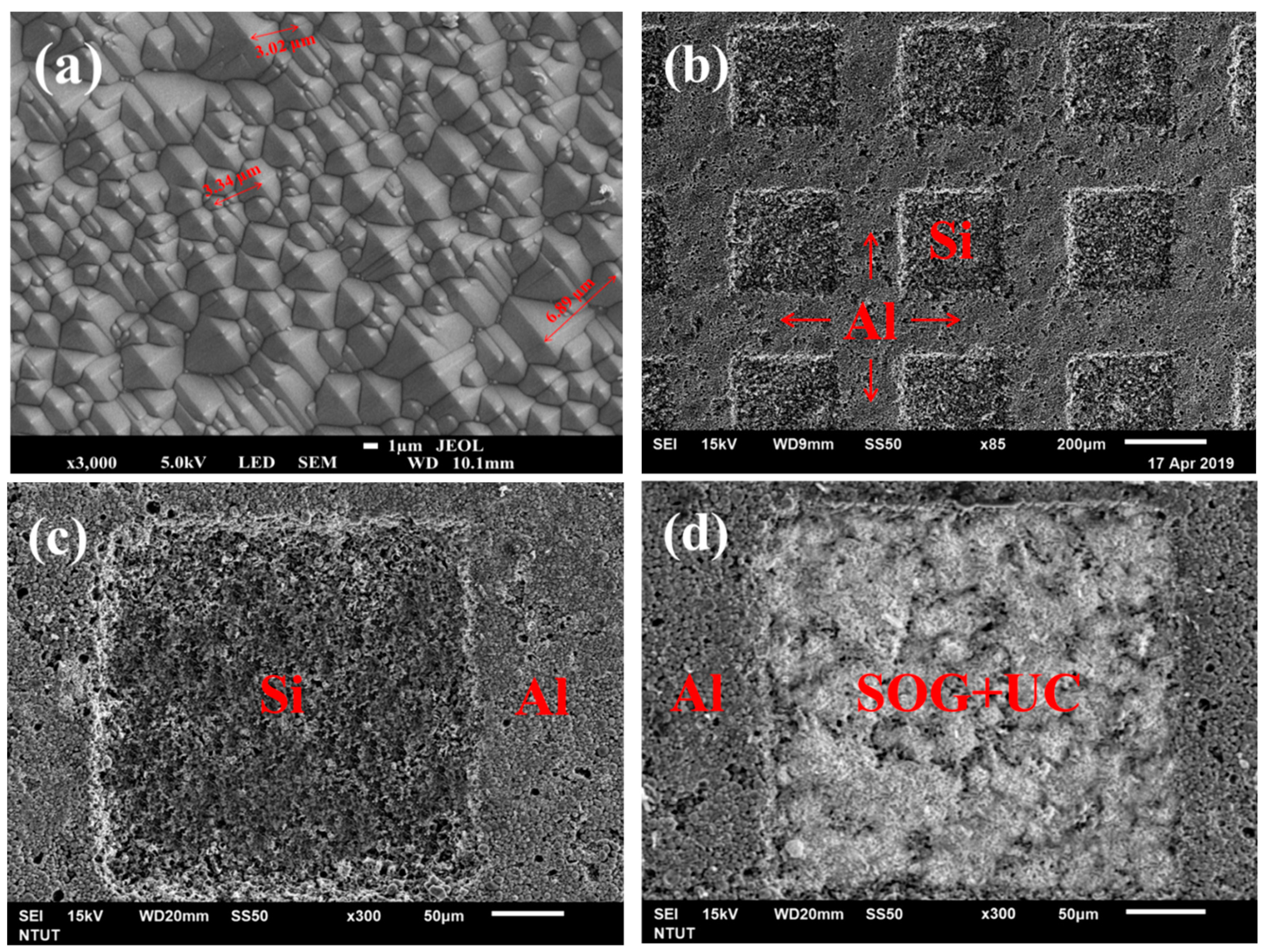
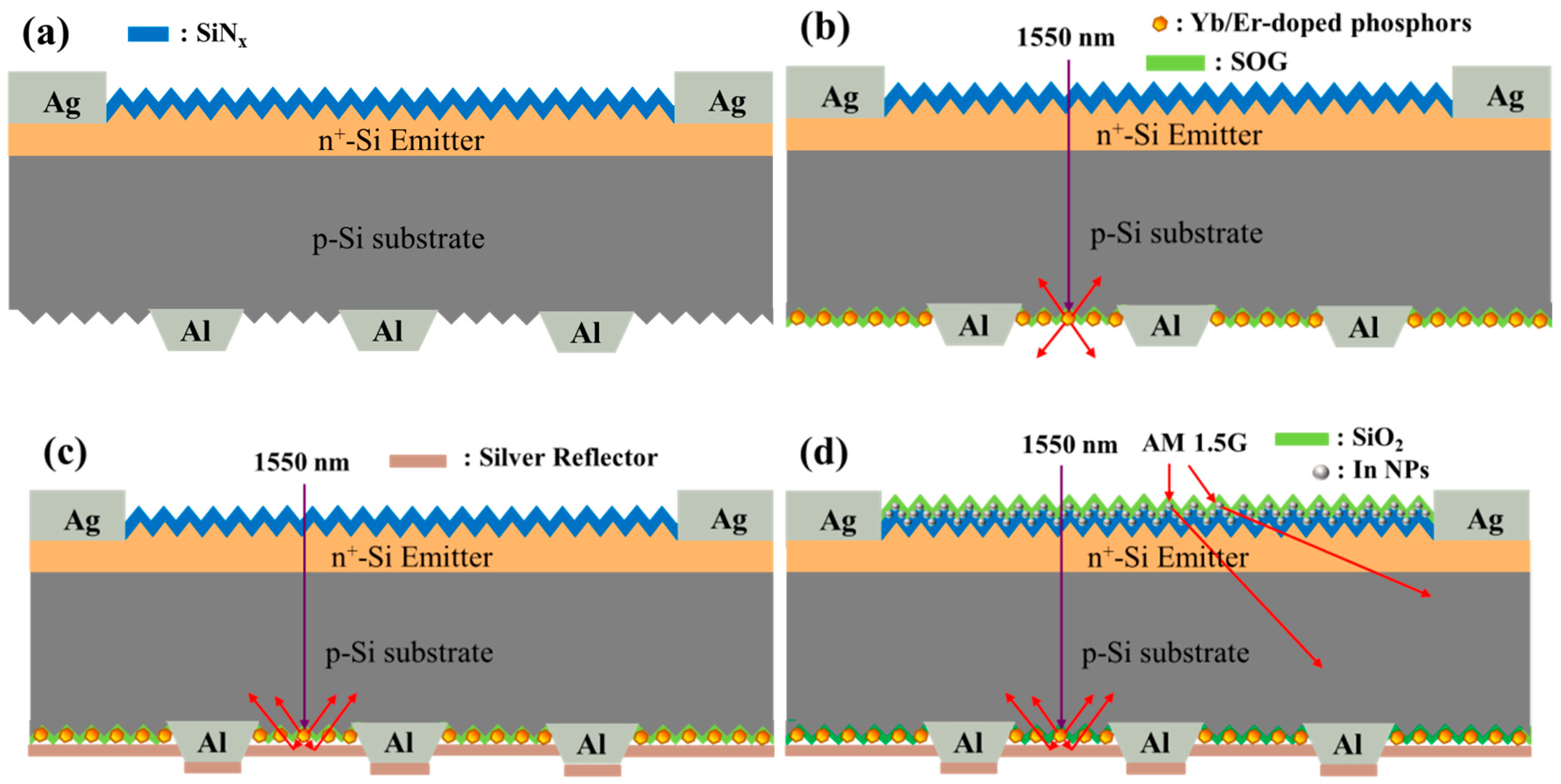
2.2. Fabrication and Characterization of Textured Silicon Solar Cells with Back Matrix Grooves

Czochralski (CZ)-grown, (100)-oriented, boron-doped single-crystalline silicon wafers (150-μm thick) with a resistivity of 10Ω·cm were cleaned using standard RCA cleaning. The surface of the silicon wafer was then etched using an anisotropic solution of H2O/KOH/IPA at 80 °C for 20 min to produce a surface texture comprising a random arrangement of pyramidal structures. Figure 2a presents a top-view SEM image showing the etched pyramidal surface. Using Image-J software, the minimum and maximum heights of the pyramids were estimated at 3 μm and 6 μm, respectively. The minimum and maximum distances between the pyramids were 3 μm and 6 μm, respectively. A 0.2-μm-thick n+-Si emitter layer with sheet resistance of approximately 80 Ω/sq (surface concentration of roughly 1.2 × 1020 cm–3) was applied to the textured silicon wafer using a POCl3 diffusion process at 810 °C over a period of 8 min. After diffusion, the phosphorous silicate glass remaining on the surface was removed using a buffered oxide etchant (BOE). A 70 nm-thick silicon nitride antireflective film was deposited on the front surface of the wafer using plasma-enhanced chemical vapor deposition. For n- and p-metallization, silver (Ag) film was deposited on the front side and aluminum (Al) film was deposited on the rear side using a screen printing process followed by drying at 200 °C. The wafer then underwent sintering (and firing) via a two-step process (ranging from 600 to 850 °C) to form finger/bus electrodes on the front side and a full Al-layer electrode on the rear side. Finally, the wafer was cut into squares (1 × 1 cm2) for use as a control substrate (hereafter referred to as bare solar cells) for further processing. After organic surface cleaning, the back surface of the bare solar cells was subjected to photolithographic etching to remove the Al film followed by a 2 wt% tetramethyl-ammonium hydroxide (TMAH) solution at 100 °C to remove residual silicon. As shown in the top-view SEM image in Figure 2b, etching resulted in matrix grooves (depth: 15 μm, width: 220 μm, length: 220 μm) with a spacing of 180 μm. Figure 2c,d respectively present grooves without any coating and with a UC layer (30 wt%). As shown in Figure 3a, the matrix-grooves covered approximately 31% of the back surface of the bare solar cells (hereafter referred to as reference cells). These samples were then characterized in terms of dark current-voltage (I-V) characteristics, optical reflectance, external quantum efficiency (EQE), and photovoltaic J-V characteristic under AM 1.5G solar simulation at room temperature.

2.3. Fabrication and Characterization of Cells Coated with Up-Conversion and Plasmonic Scattering Layers

2.3.1. Cells Coated with an Up-Conversion Layer

As shown in Figure 3b, up-conversion performance was evaluated by applying an SOG layer of SiO2 with Yb/Er-doped phosphors (YF3:Yb3+/Er3+) embedded at concentrations of 10, 20, and 30 wt% between the matrix grooves (hereafter referred to as UC cells). The methods used for UC film deposition were the same as those described in Section 2.1.1. To compensate for the isotropic emission of UC photons, we also deposited a 1-μm-thick silver film beneath the up-conversion layer as a reflector (hereafter referred to as UC/Ag cell), as shown in Figure 3c. This resulted in the reflection of down-forward UC photons back into the silicon solar cell, resulting in increased photocurrent. As a control, we also coated a silicon reference cell with the same SOG layer but without phosphors. Dark I-V, optical reflectance, EQE, and photovoltaic J-V measurements were compared with those from the reference cells to determine the contribution of the up-conversion layer.

2.3.2. Up-Conversion Combined with Plasmonic Scattering

Three up-conversion solar cells (UC/Ag cells) were coated with films of indium to depths of 3 nm, 5 nm, and 7 nm using e-beam evaporation followed by annealing in an RTA chamber under H2 at 200 °C for 20 min. This annealing process caused the transformation of the indium films into nano-sized indium particles (In NPs), over which was applied a 94 nm-thick SiO2 capping layer. As shown in Figure 3d, we characterized the UC cell with In NPs embedded in SiO2 on the front side (hereafter referred to as plasmonic UC/Ag cells) in terms of optical reflectance, EQE, and photovoltaic J-V measurements. Comparisons were made with values obtained from the UC cell in order to quantify the plasmonic effects of the In NPs. Finally, we quantified the contribution of up-conversion and plasmonic effects in enhancing the short-circuit current density and conversion efficiency of cells with In NPs (plasmonic scattering) as well as Yb/Er-doped phosphors (up-conversion).

3. Results and Discussion

3.1. Up-Conversion Layer: Characterization

Figure 4 presents the EDS spectrum obtained from the silicon substrate with a SiO2 coating containing Yb/Er-doped yttrium oxide-based phosphors (YF3:Yb3+/Er3+) at a concentration of 30 wt%. Each element within the test sample possessed a unique atomic structure, which produced a unique set of peaks in its electromagnetic emissions. EDS results revealed that the test sample comprised Y, F, O, Yb, Si, and C with small quantities of Er, Mg, and Na. Figure 5 presents the PL emission spectra obtained from a SiO2 layer containing Yb/Er-doped phosphors (YF3:Yb3+/Er3+) at concentrations of 10, 20, and 30 wt%. The excitation source was a laser diode with optical power of 500 mW and wavelength of 405 nm. The main PL emission peaks (at 670 nm, 970 nm, and 1030 nm) are indicative of the absorption peaks of silicon. PL emission intensity was shown to increase with phosphor concentration.
The up-conversion performance of the silicon solar cell coated with a layer of Yb/Er-doped phosphors was estimated in terms of up-conversion emissions and photocurrent generation. As illustrated in Figure 6a, this was achieved using optical microscope images and I-V curves obtained under illumination from a laser diode with a wavelength of 1550 nm. Figure 6b presents an optical microscope image with a red spot, which was obtained from the cell with a SiO2 layer containing Yb/Er-doped phosphors (30 wt%) under illumination from a laser diode with a wavelength of 1550 nm and optical power of 5 mW through a single-mode lensed fiber. The red emissions revealed that applying a layer of Yb/Er-doped phosphors enabled NIR up-conversion from 1550 nm to 635-690 nm, corresponding to the PL emission peaks at 670 nm (Figure 5). As shown in Figure 6c, the UC effects were confirmed by measuring the I-V characteristics of a silicon solar cell coated with a layer of Yb/Er-doped phosphors under dark and illumination conditions using a 1550 nm light source of variable power (4, 6.5, and 10 mW). Note that the dark current and photocurrent were clearly observed in the experiment, and photocurrent increased with the incident optical power. These results illustrate the contribution of an up-conversion layer when subjected to sub-bandgap illumination (i.e., light source wavelength of 1550 nm).

3.2. Plasmonic Effects of Indium Nanoparticles Imbedded in SiO2 Layer

One of the more interesting characteristics of noble metal nanoparticles is localized surface plasmon resonance (LSPR), which occurs when photons of a particular frequency induce the collective oscillation of conduction electrons on the surface of the nanoparticles. This oscillation causes the selective absorption of photons as well as efficient scattering and an increase in the strength of the electromagnetic field around the nanoparticles. Figure 7a presents the absorbance spectra (wavelength range of 200-1100 nm) of the quartz substrate, the layer of SiO2 (94 nm thick) on the quartz substrate, and the SiO2 layer (94 nm thick) with embedded In NPs (from 7 nm-thick indium film) on the quartz substrate. The absorption of the sample with In NPs embedded in the SiO2 layer was superior to that of the quartz substrate between 200 and 325 nm, with peak absorption at approximately 261 nm. The resulting absorbance spectrum revealed the LSPR absorption band and intensity of the LSPR induced by the In NPs. Figure 7b presents the Raman spectra of the quartz substrate coated using a SiO2 layer with embedded In NPs of various sizes (3 nm, 5 nm, and 7 nm). The samples with In NPs presented shifts in Raman peaks at 875 and 1500 cm-1, compared to the quartz substrate. Note that peaks in the Raman signal from noble metal nanoparticles are generally an indication of LSPR under a light source of specific wavelength [39]. Measurements were also obtained from the sample without In NPs to confirm the plasmonic effects of the In NPs embedded in the SiO2 layer. Note also that we observed an increase in the intensity of the Raman signals with an increase in the size of the In NPs. Plasmonic effects were particularly evident in the sample with larger In NPs (7 nm).

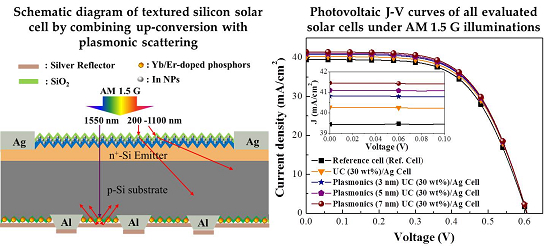
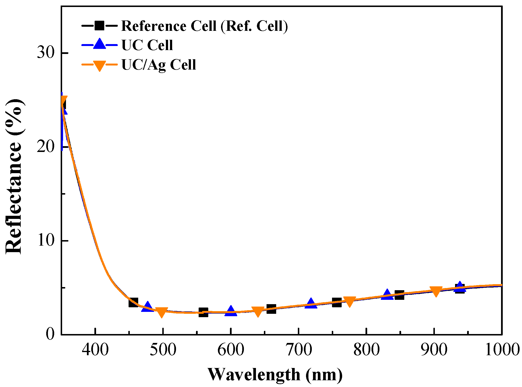
3.3. Reference Textured Silicon Solar Cell and Up-Conversion Solar Cells

Figure 8 presents the dark I-V curves obtained from the reference textured silicon solar cell, UC cell, and UC/Ag cell. The reverse saturation current-density (J0) and ideality factor (n) values were extracted from the dark I-V curves to evaluate the surface states and passivation performance of the proposed solar cell. The reverse saturation (J0) and n values were as follows: reference textured silicon solar cell (8.62 × 10⁻⁷ A/cm2 and 2.38), UC cell (4.23 × 10⁻⁷ A/cm2, 2.30), and UC/Ag cell (6.76 × 10⁻⁷ A/cm2, 2.36). The reductions in J0 and n indicate the contribution of the SiO2 and/or passivation effects from Yb/Er-doped phosphors on the back-side surface of the cells. These results can be attributed to the suppression of surface carrier recombination on the matrix-grooved surface by the SiO2 layer containing Yb/Er-doped phosphors. Figure 9 presents the measured optical reflectance of the reference cell, UC cell, and UC/Ag cell. The average weighted reflectance (RW) values (3.73 %) were calculated over a wavelength range of 350 to 1000 nm. The optical reflectance values of the UC cell and UC/Ag cell were the same as those of the reference cell. This can be attributed to the absence of photons reflected from the UC layer and Ag-reflector, thereby indicating the absorption of all incident photons (350–1000 nm wavelengths) in the 150-μm-thick silicon layer.
In this study, EQE data were obtained by adjusting the incident light from long wavelengths (1000 nm) to short wavelengths (350 nm). Figure 10 presents the EQE response of the reference cell, UC cell, and UC/Ag cell with phosphor concentrations of (a) 10 wt%, (b) 20 wt%, and (c) 30 wt%. The inset in Figure 10 illustrates the enhanced up-conversion performance at wavelengths between 960 and 1000 nm, in samples with various phosphor concentrations. The best EQE performance was obtained from the samples with a phosphor concentration of 30 wt%. Table 1 lists the average external quantum efficiency (EQEW) calculated at wavelengths between 350 and 1000 nm. For the sake of clarity, we calculated the EQEW of the cells as follows:
E Q E W = 350   n m 1000   n m E Q E ( λ ) p h ( λ ) d λ 350   n m 1000   n m p h ( λ ) d λ × 100 %
where EQE(λ) indicates the external quantum efficiency at a given wavelength (λ) and φph (λ) is the photon flux of AM 1.5G at the same wavelength (λ). The EQEW of the reference cell was 87.27%. We obtained higher EQEW values from the UC cell (87.41–87.63%), due to the up-conversion of photons by Yb/Er-doped phosphors, and the UC/Ag cell (87.46–87.86%) due to the generation of additional photocurrent from UC photons reflected by the Ag. The highest EQEW values were obtained from the UC cell and UC/Ag cell with a phosphor concentration of 30 wt%. These EQEW results were subsequently used as a baseline to evaluate the performance of cells with an up-conversion layer or a combination of up-conversion and plasmonic scattering layers.
Figure 11 presents the EQE enhancement (ΔEQE) of (a) the reference cell with an Ag reflector relative to that of the reference cell (violet line) and (b) the UC/Ag cell at phosphor concentrations of 30 wt% relative to that of the reference cell (orange line). We observed that an increase in the ΔEQE values of the reference cell with an Ag reflector at wavelengths of 800–1000 nm, due to the absorption of photons of long wavelength (> 800 nm). Note that these photons were transmitted to the rear surface of the silicon cell (a distance of 150-μm) and then reflected back into the silicon by the Ag reflector. The re-absorption of the reflected photons by the silicon also led to the generation of additional photocurrent. The UC cell with an Ag reflector also presented an increase in EQE intensity with two peaks in the ΔEQE spectrum (920, 980 nm). Overall, these results can be attributed to the back-scattering of photons by Yb/Er-doped phosphor particles and the effects of up-conversion from near-infrared to the visible spectrum by Yb/Er-doped phosphors under excitation from transmitted photons with a wavelength of approximately 980 nm. The EQE enhancement in the current study was small. However, our results demonstrate the possibility of using Yb/Er-doped phosphors as an up-conversion vehicle to enhance the efficiency of thin silicon solar cells (150-μm).
Figure 12 presents photovoltaic J-V curves obtained from the reference cell, UC cell, and UC/Ag cell with Yb/Er-doped phosphors at a concentration of 30 wt% in the UC layer. Table 2 lists the photovoltaic performance of the reference cell, UC cell, and UC/Ag cell. Under AM 1.5G solar simulation at room temperature, the photovoltaic performance of the reference cell was as follows: open-circuit voltage (Voc) of 604.7 mV, short-circuit current-density (JSC) of 39.43 mA/cm2, and conversion efficiency (η) of 14.45%. The layer of Yb/Er-doped phosphors increased the JSC and η of the UC cell to 40.08 mA/cm2 and 14.82%, respectively. Using a layer of Yb/Er-doped phosphors in conjunction with an Ag reflector resulted in the highest JSC (40.29 mA/c m2) and η (14.94%). Note that the UC/Ag cell outperformed the UC cell in this regard. These results indicate that the up-conversion provided Yb/Er-doped phosphors in the SiO2 layer enhanced the photovoltaic performance of the solar cells. For the sake of clarity, we calculated the JSC value of UC cell and UC/Ag cell as follows:
J S C = J S C R e f + Δ J S C U C + Δ J S C U C / A g
where JSC-Ref is the JSC value of the reference cell, ΔJSC-UC is the increase in JSC due to the up-conversion of photons by Yb/Er-doped phosphors, and ΔJSC-UC/Ag is the increase in JSC value due to the up-conversion of photons by Yb/Er-doped phosphors as well as the reflection of photons by the Ag reflector. The results obtained from the UC (30 wt%)/Ag (1 μm) solar cell were subsequently used as a baseline in evaluating the performance of cells with a combination of up-conversion and plasmonic scattering layers.

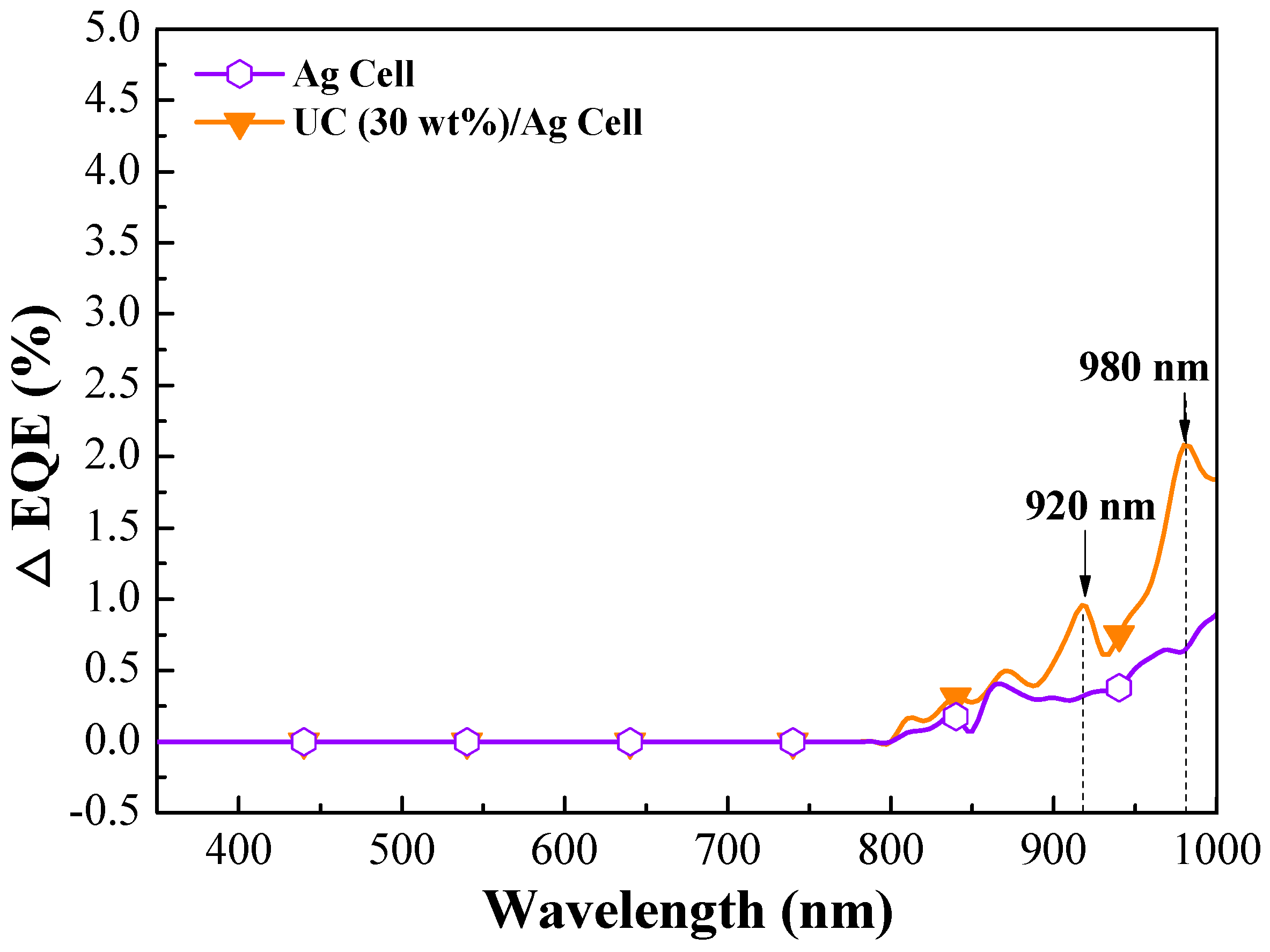
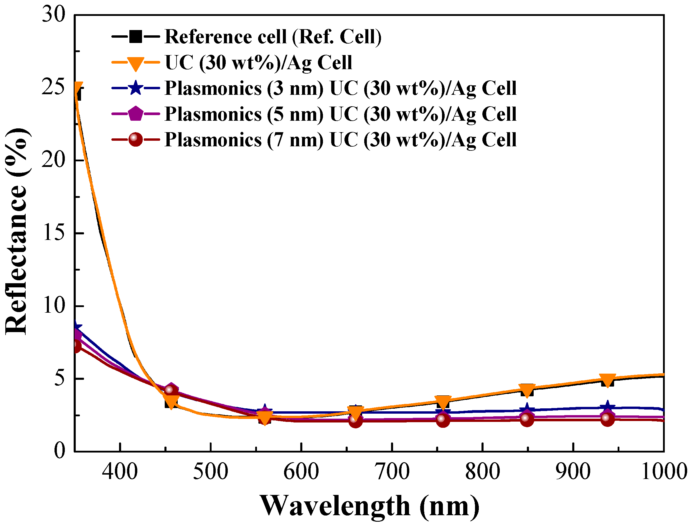
3.4. Textured Silicon Solar Cells with Up-Conversion and Plasmonic Scattering Layers

Figure 13 presents the optical reflectance of the reference cell, UC (30 wt%)/Ag cell, and plasmonic UC (30 wt%)/Ag cell with In NPs (3 nm, 5 nm, and 7 nm). The reflectance of the plasmonic UC (30 wt%)/Ag cell was lower that of the reference cell and UC (30 wt%)/Ag cell at the wavelength ranges of 350-450 nm and 650-1000 nm. This can be attributed to plasmonic forward scattering induced by the In NPs. The lowest reflectance was observed in the plasmonic UC/Ag cell with In NPs (7 nm). The reflectance of the plasmonic UC/Ag cell was also slightly higher than that of the reference cell and UC/Ag cell (without a SiO2 layer on the front side) at wavelengths between 450 and 550 nm. This can be attributed to the fact that the SiO2/SiNx layer was not of optimal thickness, such that reflectance and destructive interference could not be minimized in this wavelength band. The RW values of the cells are listed in Table 1.
Figure 14a presents the EQE of the reference cell, UC (30 wt%)/Ag cell and plasmonic UC (30 wt%)/Ag cell with In NPs (3 nm, 5 nm, and 7 nm). The EQE response values are in good agreement with the optical reflectance values. The EQE value of the plasmonic UC cells increased with an increase in the size of the In-NPs. For the sake of clarity, we calculated the EQETotal value of the plasmonic UC cell as follows:
E Q E T o t a l = E Q E R e f + Δ E Q E U C + Δ E Q E S c a t   I n N P s
where EQERef is the EQE value of the reference cell, ΔEQEUC is the EQE enhancement attributable to the up-conversion layer, and ΔEQEUC+Scat is the EQE enhancement attributable to the up-conversion layer plus the plasmonic scattering layer. Table 1 lists the EQEW values of all cells evaluated in this experiment. The highest EQEW value (88.94%) was obtained from the plasmonic UC cell with In NPs of larger diameter (7 nm). Figure 14b presents the internal quantum efficiency (IQE) response of the reference cell, UC (30 wt%)/Ag cell, and plasmonic UC (30 wt%)/Ag cell with In NPs (3 nm, 5 nm, and 7 nm), illustrating the influence of plasmonic particles on cell parameters.
Figure 15 presents EQE enhancement (ΔEQE) spectra of the UC (30 wt%)/Ag cell and plasmonic UC (30 wt%)/Ag cell with In NPs (3 nm, 5 nm, 7 nm), versus the values obtained from the reference cell. The EQE response of the plasmonic UC (30 wt%)/Ag cell with In NPs exceeded that of the UC/Ag cell across a wide range of wavelengths, due to plasmonic scattering induced by In NPs and up-conversion by Yb/Er-doped phosphors. Note also that we observed a considerable increase in EQE due to the backscattering of photons by Yb/Er-doped phosphors in the plasmonic UC (30 wt%)/Ag cell with 7 nm In NPs.
Figure 16 presents the photovoltaic J-V curves of the reference cell, UC (30 wt%)/Ag cell and the plasmonic UC (30 wt%)/Ag cells with In NPs (3 nm, 5 nm, and 7 nm). Table 2 lists the photovoltaic performance of all evaluated cells to compare the effects of up-conversion, plasmonic scattering, and a combination of up-conversion with plasmonic scattering. The JSC and η values were as follows: plasmonic UC/Ag cell with In NPs (3 nm) (JSC = 40.82 mA/cm2, η =15.19%), plasmonic UC/Ag cell with In NPs (5 nm) (JSC = 41.11 mA/cm2, η =15.32%) and plasmonic UC/Ag cell with In NPs (7 nm) (JSC = 41.46 mA/cm2, η =15.43%). Significant increases in JSC and η values were obtained when using In NPs of larger size. For the sake of clarity, we calculated the JSC value of plasmonic UC cell as follows
J S C = J S C R e f + Δ J S C U C / A g + Δ J S C S c a t I n N P s
where JSC-Ref is the JSC value of the reference cell, ΔJSC-UC/Ag is the JSC enhancement attributable to the up-conversion layer and Ag reflector, and ΔJSC-Scat-In NPs is the JSC enhancement attributable to the plasmonic scattering layer.
In summary, we obtained impressive improvements in the JSC and η values of the UC/Ag cell (ΔJSC= 2.18%, Δη = 3.39%, compared to reference cell), due to the up-conversion effects of the Yb/Er-doped phosphors. Notable improvements were observed in the cell with In NPs (7 nm) (ΔJSC= 2.90%, Δη = 3.28%, compared to reference cell), due to the plasmonic scattering of the In NPs. Further improvements were observed in the plasmonic UC/Ag cell with the In NPs (7 nm) and UC (30 wt%) layers (ΔJSC = 5.15%, Δη = 6.78%, compared to the reference cell), due to the combination of plasmonic scattering and up-conversion effects.

4. Conclusions

This study examined the up-conversion characteristics of Yb/Er-doped yttrium oxide-based phosphors embedded in a SiO2 layer as well as the plasmonic effects of indium nanoparticles embedded (at various concentrations) in a SiO2 layer. We also examined the conversion performance of textured silicon solar cells with an up-conversion layer, a plasmonic scattering layer, or a combination of up-conversion and plasmonic-scattering layers. Compared to a reference silicon solar cell, depositing a layer of SiO2 containing 30 wt% Yb/Er-doped yttrium oxide-based phosphors and a silver reflector improved conversion efficiency by 3.39%, whereas applying that same up-conversion layer and plasmonic-scattering layer of In NPs improved conversion efficiency by 6.78%, due to the combination of up-conversion plus plasmonic scattering effects. The absolute conversion efficiency of the textured silicon solar cell with a combination of up-conversion and plasmonic-scattering layers (15.43%) exceeded that of the cell with an up-conversion layer only (14.94%) and that of the reference cell (14.45%).

Author Contributions

All of the authors conceived the experiments; W.-J.H. designed, analyzed, and wrote the first draft of the paper; W.-C.L. and J.-J.L. performed the experiments; H.-J.S. and C.-F.L. conducted EQE measurements; all authors contributed to the discussion.

Funding

The authors would like to thank the Ministry of Science and Technology of the Republic of China for financial support under Grant MOST 106-2221-E-027-101-MY3.

Conflicts of Interest

The authors declare no conflict of interest.

References

  1. Mennucci, C.; Muhammad, M.H.; Hameed, M.F.O.; Mohamed, S.A.; Abdelkhalik, M.S.; Obayya, S.S.A.; de Mongeot, F.B. Broadband light trapping in nanotextured thin film photovoltaic devices. Appl. Surf. Sci. 2018, 446, 74–82. [Google Scholar] [CrossRef]
  2. Green, M.A.; Bremner, S.P. Energy conversion approaches and materials for high-efficiency photovoltaics. Nat. Mater. 2017, 16, 23–34. [Google Scholar] [CrossRef]
  3. Lu, P.; Xu, J.; Cao, Y.Q.; Lai, J.W.; Xu, L.; Chen, K.J. Preparation of nano-patterned Si structures for hetero-junction solar cells. Appl. Surf. Sci. 2015, 334, 123–128. [Google Scholar] [CrossRef]
  4. Zhang, D.; Ren, W.N.; Zhu, Z.C.; Zhang, H.F.; Liu, B.; Shi, W.Z.; Qin, X.M.; Cheng, C.W. Highly-ordered silicon inverted nanocone arrays with broadband light antireflectance. Nanoscale Res. Lett. 2015, 10, 1–6. [Google Scholar] [CrossRef] [Green Version]
  5. Liu, D.M.; Wang, Q.K.; Wang, Q. Transfer the multiscale texture of crystalline Si onto thin-film micromorph cell by UV nanoimprint for light trapping. Appl. Surf. Sci. 2018, 439, 168–175. [Google Scholar] [CrossRef]
  6. Araújo, A.; Mendes, M.J.; Mateus, T.; Costa, J.; Nunes, D.; Fortunato, E.; Águas, H.; Martins, R. Ultra-fast plasmonic back reflectors production for light trapping in thin Si solar cells. Sol. Energy 2018, 174, 786–792. [Google Scholar] [CrossRef]
  7. Rao, L.; Ji, C.L.; Li, M. Broadband light absorption of silicon nanowires embedded in Ag nano-hole arrays. AIP Adv. 2016, 6, 095216. [Google Scholar] [CrossRef] [Green Version]
  8. Veenkamp, R.J.; Ye, W.N. Plasmonic metal nanocubes for broadband light absorption enhancement in thin-film a-Si solar cells. J. Appl. Phys. 2014, 115, 124317. [Google Scholar] [CrossRef]
  9. Atwater, H.A.; Polman, A. Plasmonics for improved photovoltaic devices. Nat. Mater. 2010, 9, 205–213. [Google Scholar] [CrossRef]
  10. Garcia, M.A. Surface plasmons in metallic nanoparticles: Fundamentals and applications. J. Phys. D Appl. Phys. 2011, 44, 283001. [Google Scholar] [CrossRef]
  11. Kelly, K.L.; Coronado, E.; Zhao, L.L.; Schatz, G.C. The optical properties of metal nanoparticles: The influence of size, shape, and dielectric environment. J. Phys. Chem. B 2003, 107, 668–677. [Google Scholar] [CrossRef]
  12. Derkacs, D.; Lim, S.H.; Matheu, P.; Mar, W.; Yu, E.T. Improved performance of amorphous silicon solar cells via scattering from surface plasmon polaritons in nearby metallic nanoparticles. Appl. Phys. Lett. 2006, 89, 093103. [Google Scholar] [CrossRef] [Green Version]
  13. Pedrueza, E.; Sancho-Parramon, J.; Bosch, S.; Valdés, J.L.; Martinez-Pastor, J.P. Plasmonic layers based on Au-nanoparticle-doped TiO2 for optoelectronics: Structural and optical properties. Nanotechnology 2013, 24, 065202. [Google Scholar] [CrossRef] [PubMed]
  14. Lee, S.K.; Tan, C.L.; Lee, Y.T. Light trapping enhancement induced by bimetallic non-alloyed nanoparticles on a disordered subwavelength flexible thin film crystalline silicon substrate using metal-assisted chemical etching. Opt. Lett. 2017, 42, 431–434. [Google Scholar] [CrossRef] [PubMed]
  15. Tan, H.; Santbergen, R.; Yang, G.; Smets, A.H.M.; Zeman, M. Combined optical and electrical design of plasmonic back reflector for high-efficiency thin-film silicon solar cells. IEEE J. Photovolt. 2013, 3, 53–58. [Google Scholar] [CrossRef]
  16. Tong, C.; Yun, J.; Song, H.; Gan, Q.; Anderson, W.A. Plasmonic-enhanced Si schottky barrier solar cells. Sol. Energy Mater. Sol. Cells 2014, 120, 591–595. [Google Scholar] [CrossRef]
  17. Lesina, A.C.; Paternoster, G.; Mattedi, F.; Ferrario, L.; Berini, P.; Ramunno, L.; Paris, A.; Vaccari, A.; Calliari, L. Modeling and characterization of antireflection coatings with embedded silver nanoparticles for silicon solar cells. Plasmonics 2015, 10, 1525–1536. [Google Scholar] [CrossRef]
  18. Manai, L.; Rezgui, B.D.; Zaghouani, R.B.; Barakel, D.; Torchio, P.; Palais, O.; Bessais, B. Tuning of light trapping and surface plasmon resonance in silver nanoparticles/c-Si structures for solar cells. Plasmonics 2016, 11, 1273–1277. [Google Scholar] [CrossRef]
  19. Araújo, A.; Mendes, M.J.; Mateus, T.; Vicente, A.; Nunes, D.; Calmeiro, T.; Fortunato, E.; Águas, H.; Martins, R. Influence of the substrate on the morphology of self-assembled silver nanoparticles by rapid thermal annealing. J. Phys. Chem. C 2016, 120, 18235–18242. [Google Scholar] [CrossRef]
  20. Zhang, Y.N.; Chen, X.; Ouyang, Z.; Lu, H.Y.; Jia, B.H.; Shi, Z.R.; Gu, M. Improved multicrystalline Si solar cells by light trapping from Al nanoparticle enhanced antireflection coating. Opt. Mater. Express 2013, 3, 489–495. [Google Scholar] [CrossRef]
  21. Temple, T.L.; Bagnall, D.M. Optical properties of gold and aluminium nanoparticles for silicon solar cell applications. J. Appl. Phys. 2011, 109, 084343. [Google Scholar] [CrossRef] [Green Version]
  22. Parashar, P.K.; Sharma, R.P.; Komarala, V.K. Mediating broad band light trapping in silicon solar cell by aluminum nanoparticles with native oxide shell. Mater. Today Proc. 2017, 4, 12708–12715. [Google Scholar] [CrossRef]
  23. Couderc, R.; Amara, M.; Lemiti, M. In-depth analysis of heat generation in silicon solar cells. IEEE J. Photovolt. 2016, 6, 1123–1131. [Google Scholar] [CrossRef]
  24. Shockley, W.; Queisser, H.J. Detailed balance limit of efficiency of p-n junction solar cells. J. Appl. Phys. 1961, 32, 510–519. [Google Scholar] [CrossRef]
  25. Tayebjee, M.J.Y.; Rao, A.; Schmidt, T.W. All-optical augmentation of solar cells using a combination of up- and downconversion. J. Photonics Energy 2018, 8, 022007. [Google Scholar] [CrossRef]
  26. Ho, W.J.; Shen, Y.T.; Liu, J.J.; You, B.J.; Ho, C.H. Enhancing photovoltaic performance using broadband luminescent down-shifting by combining multiple species of Eu-doped silicate phosphors. Nanomaterials 2017, 7, 340. [Google Scholar] [CrossRef]
  27. Tahhan, A.; Dehouche, Z.; Fern, G.R.; Haverkamp, E. Photovoltaic cells energy performance enhancement with down-converting photoluminescence phosphors. Int. J. Energy Res. 2015, 39, 1616–1622. [Google Scholar] [CrossRef] [Green Version]
  28. Ho, W.J.; Yang, G.C.; Shen, Y.T.; Deng, Y.J. Improving efficiency of silicon solar cells using europium-doped silicate-phosphor layer by spin-on film coating. Appl. Surf. Sci. 2016, 365, 120–124. [Google Scholar] [CrossRef]
  29. Huang, X.; Liu, J.M.; Pan, H.; Tian, C.C.; Zhang, H.; Chen, X.J.; Huang, A.P.; Xiao, Z.S. Temperature-dependent upconversion luminescence and spectra characteristic of Er3+/Yb3+ co-doped fluorotellurite glasses. J. Lumines. 2019, 207, 41–47. [Google Scholar] [CrossRef]
  30. Castro, T.; Manzani, D.; Ribeiro, S.J.L. Up-conversion mechanisms in Er3+-doped fluoroindate glasses under 1550 nm excitation for enhancing photocurrent of crystalline silicon solar cell. J. Lumines. 2018, 200, 260–264. [Google Scholar] [CrossRef]
  31. Takeda, Y.; Luitel, H.N.; Mizuno, S. Competing effects of sensitization and energy dissipation by Ni2+ incorporation in La(Ga0.5Sc0.5)O3:Er,Ni,Nb upconverters. J. Lumines. 2018, 194, 778–784. [Google Scholar] [CrossRef]
  32. Luitel, H.N.; Mizuno, S.; Tani, T.; Takeda, Y. Broadband-sensitized upconversion of ATiO3:Er,Ni (A = Mg, Ca, Sr, Ba). J. Ceram. Soc. Jpn. 2017, 125, 821–828. [Google Scholar] [CrossRef]
  33. van Sark, W.G.; de Wild, J.; Rath, J.K.; Meijerink, A.; Schropp, R.E. Upconversion in solar cells. Nanoscale Res. Lett. 2013, 8, 1–10. [Google Scholar] [CrossRef] [PubMed]
  34. Huang, X.Y.; Han, S.Y.; Huang, W.; Liu, X.G. Enhancing solar cell efficiency: The search for luminescent materials as spectral converters. Chem. Soc. Rev. 2013, 42, 173–201. [Google Scholar] [CrossRef] [PubMed]
  35. Richards, B.S.; Shalav, A. Enhancing the near-infrared spectral response of silicon optoelectronic devices via up-conversion. IEEE Trans. Electron Devices 2007, 54, 2679–2684. [Google Scholar] [CrossRef]
  36. Ho, W.J.; Liu, J.J.; Yang, Y.C.; Ho, C.H. Enhancing output power of textured silicon solar cells by embedding indium plasmonic nanoparticles in layers within antireflective coating. Nanomaterials 2018, 8, 1003. [Google Scholar] [CrossRef]
  37. Ho, W.J.; Lin, J.C.; Liu, J.J.; Yeh, C.W.; Syu, H.J.; Lin, C.F. Plasmonic light scattering in textured silicon solar cells with indium nanoparticles from normal to non-normal light incidence. Materials 2017, 7, 737. [Google Scholar] [CrossRef]
  38. Ho, W.J.; Wei, C.Y.; Liu, J.J.; Lin, W.C.; Ho, C.H. Performance characterization of planar silicon solar cells using NIR up-conversion layer comprising YF3:Yb3+/Er3+ phosphors. Vacuum 2019, 166, 1–5. [Google Scholar] [CrossRef]
  39. Das, R.; Soni, R.K. Indium nanoparticles for ultraviolet surface-enhanced Raman spectroscopy. AIP Conf. Proc. 2018, 1953, 030123. [Google Scholar] [CrossRef]
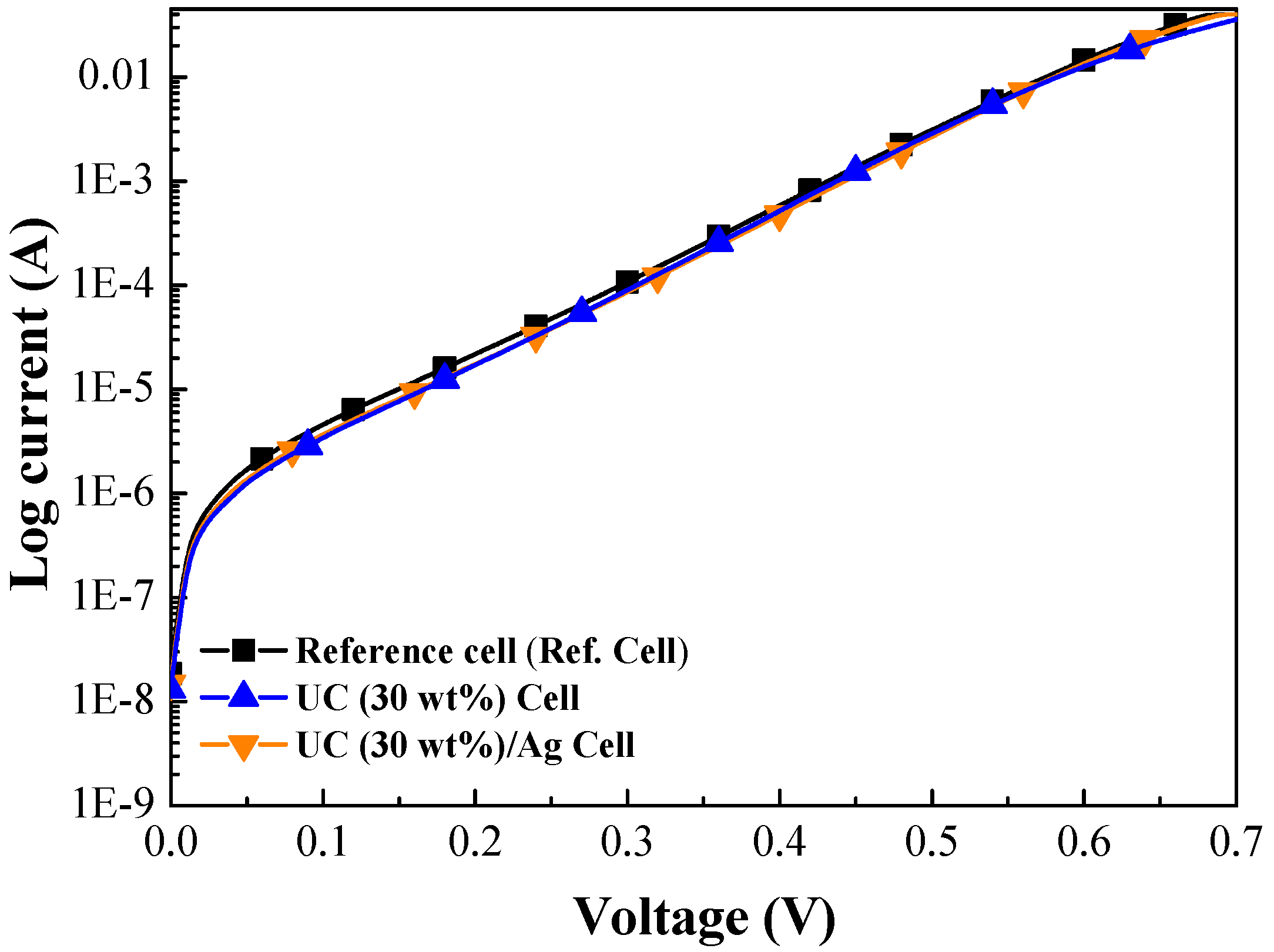
Figure 1. Schematic diagram of the test sample with (a) up-conversion (UC) layer and (b) SiO2 layer with embedded indium nanoparticles (In NPs).
Energies 12 04119 g001
Figure 2. Top-view SEM images of (a) etched pyramidal surface, (b) etched matrix-grooves, (c) grooves without coating, and (d) grooves coated with the UC layer.
Energies 12 04119 g002
Figure 3. Schematic diagram showing (a) reference cell, (b) up-conversion (UC) cell, (c) UC cell with silver reflector (UC/Ag cell), (d) UC/Ag cell with In NPs embedded in SiO2 (plasmonic UC/Ag cell).
Energies 12 04119 g003
Figure 4. Energy-dispersive X-ray spectroscopy (EDS) spectrum obtained from SiO2 coating containing Yb/Er-doped yttrium oxide-based phosphors (YF3:Yb3+/Er3+).
Energies 12 04119 g004
Figure 5. Photoluminescence (PL) emission spectra of SiO2 layer containing Yb/Er-doped phosphors (YF3:Yb3+/Er3+) at concentrations of 10, 20, and 30 wt%.
Energies 12 04119 g005
Figure 6. (a) Schematic diagram showing measurement set up to estimate up-conversion performance, (b) Optical microscope image showing red spot from Yb/Er-doped phosphors illuminated by laser diode with wavelength of 1550 nm and optical power of 5 mW, (c) I-V characteristics of proposed silicon solar cell coated with an Yb/Er-doped phosphors layer under dark illumination conditions using 1550 nm light source of variable power.
Energies 12 04119 g006aEnergies 12 04119 g006b
Figure 7. (a) Absorbance spectra of bare quartz substrate and quartz substrate coated with SiO2 layer containing In NPs of various sizes (3 nm, 5 nm, and 7 nm), (b) Raman scattering spectrum of bare quartz substrate and quartz substrate coated with SiO2 layer containing In NPs of various sizes (3 nm, 5 nm, and 7 nm).
Energies 12 04119 g007
Figure 8. Dark I-V curves of the reference cell, UC cell, and UC/Ag cell.
Energies 12 04119 g008
Figure 9. Optical reflectance of reference solar cell, UC cell, and UC/Ag cell.
Energies 12 04119 g009
Figure 10. External quantum efficiency (EQE) response of reference cell, UC cell, and UC/Ag cell at phosphor concentration of (a) 10 wt%, (b) 20 wt%, (c) 30 wt %.
Energies 12 04119 g010
Figure 11. EQE enhancement (ΔEQE) of (a) reference cell with Ag reflector relative to that of the reference cell (violet line) and (b) UC/Ag cell at a phosphor concentration of 30 wt% relative to that of the reference cell (orange line).
Energies 12 04119 g011
Figure 12. Photovoltaic J-V of reference cell, UC cell (30 wt%), and UC (30 wt%)/Ag cell.
Energies 12 04119 g012
Figure 13. Optical reflectance of the reference cell, UC (30 wt%)/Ag cell and plasmonic UC (30 wt%)/Ag cell with In NPs (3 nm, 5 nm, 7 nm).
Energies 12 04119 g013
Figure 14. (a) EQE response and (b) internal quantum efficiency (IQE) response of reference cell, UC (30 wt%)/Ag cell, and plasmonic UC (30 wt%)/Ag cell with In NPs (3 nm, 5 nm, 7 nm).
Energies 12 04119 g014
Figure 15. EQE enhancement of UC (30 wt%)/Ag cell and plasmonic UC (30 wt%)/Ag cell with In NPs (3 nm, 5 nm, 7 nm) respectively compared with the reference cell.
Energies 12 04119 g015
Figure 16. Photovoltaic J-V curves of reference cell, UC (30 wt%)/Ag cell, and plasmonic UC (30 wt%)/Ag cells with In NPs (3 nm, 5 nm, 7 nm).
Energies 12 04119 g016
Table 1. Ideality factor (n), reverse saturation current density (J0), average weighted reflectance (RW), and average external quantum efficiency (EQEW).
Silicon Solar CellIdeality Factor (n)Reverse Saturation Current Density (J0, A/cm2)RW (%)
@ 350–1000 nm
EQEW (%)
@ 350–1000 nm
Reference Cell (Ref. Cell)2.388.62 × 10–73.7387.27
UC (10 wt%) Cell2.315.51 × 10–73.7387.41
UC (20 wt%) Cell2.325.47 × 10–73.7387.50
UC (30 wt%) Cell2.304.23 × 10–73.7387.63
UC (10 wt%)/Ag Cell2.377.08 × 10–73.7387.46
UC (20 wt%)/Ag Cell2.378.04 × 10–73.7387.71
UC (30 wt%)/Ag Cell2.366.76 × 10–73.7387.86
Plasmonic (7 nm) UC/Ag Cell2.265.36 × 10–73.6288.94
Table 2. Photovoltaic performances of all evaluated solar cells.
For UC ComparisonVoc
(mV)
JSC
(mA/cm2)
F.F. (%)η
(%)
ΔJSC
(%)
Δη (%)
Reference Cell (Ref. Cell)604.739.4360.614.45----
UC (30 wt%) Cell608.640.0860.714.821.652.56
UC (30 wt%)/Ag Cell608.040.2961.014.942.183.39
Comparison of plasmonic effects------------
UC (30 wt%)/Ag Cell608.040.2961.014.94----
Plasmonic (3 nm) UC/Ag Cell608.240.8261.215.191.321.67
Plasmonic (5 nm) UC/Ag Cell608.141.1161.315.322.042.54
Plasmonic (7 nm) UC/Ag Cell608.341.4661.215.432.903.28
Comparison of UC and Plasmonic Effects------------
Reference Cell (Ref. Cell)604.739.4360.614.45----
UC (30 wt%) Cell608.640.0860.714.821.652.56
UC (30 wt%)/Ag Cell608.040.2961.014.942.183.39
Plasmonic (3 nm) UC/Ag Cell608.240.8261.215.193.535.12
Plasmonic (5 nm) UC/Ag Cell608.141.1161.315.324.266.02
Plasmonic (7 nm) UC/Ag Cell608.341.4661.215.435.156.78

