1. Introduction
At present, photovoltaic (PV) systems has been consolidated as a strong alternative for using renewable energy sources. This is due to the improvement in the efficiency of the solar cells, the growing number of manufacturers of PV technology and the different types of PV modules available in the markets [
1,
2,
3]. PV systems transform the sunlight into electricity to feed a load and they are formed by arrays of PV modules, which are connected in series or parallel depending on the voltage and current required by the load [
4]. Typically, PV modules are formed by two or more submodules in series connection. Each submodule is formed by a group of series connected cells, which in turn are all connected in anti-parallel with a protection diode known as bypass diode [
5,
6].
In a PV module, a submodule may operate in reduced irradiance conditions due to external factors as shadows or dirt on the surface of the module. When that happens, the maximum current delivered by the submodule (short-circuit current) is lower to the short-circuit currents of the other submodules in the module. Then, when the current delivered by the module is higher than the short-circuit current of the shaded submodule, the excess of current flows through the submodule’s bypass diode. In such a way, the current and power delivered by the module is not constrained to the operation conditions of the shaded submodule [
5]. However, the activation of the bypass diode provokes inflections points in the I-V curve and multiple peaks in the power-voltage (P-V) curves of the module and arrays [
7,
8]. Therefore, the bypass diodes play an important role in the operation and the modeling of PV modules [
9].
In literature, different approaches for modeling bypass diodes has been reported: the ideal model, the piecewise linear model and the exponential model. The simplest model is to represent the bypass diode as an ideal switch [
10]; nevertheless, in such a representation the voltage drops of the diodes, when they become active, are not considered. Another approach is the piecewise linear model in which the diode is represented by series connection of a voltage source, a resistance and an ideal switch [
10]. The piecewise linear and the ideal model require an operating point (i.e., voltage and current) of the PV submodule in which the diode becomes active, therefore, their use is complex for modeling a PV module [
11,
12]. The exponential model uses the Schottky equation including its behavior in the first and second quadrant. This model is more accurate than ideal and piecewise linear models and it does not require the definition of an operating point in which the diode becomes active, however such a model is non-linear and more complex.
The parameters required to represent the bypass diode depend on the model. In this way, in the piecewise linear model, the value of the voltage source and the resistance are required, while in the exponential model two parameters are needed: the inverse saturation current and the ideality factor. At present, the authors have not found a detailed procedure to estimate the parameters of a bypass diode in a PV module. However, in literature there are some works related with calculating the parameters of a PV module [
13,
14,
15], procedures to identify damages in the bypass diodes [
16,
17,
18] and methods for estimating the parameters of Schottky diode [
19,
20,
21].
In [
15], some techniques for the extraction of the single and double diode model parameters of a PV submodule are presented. Such a work shows that some techniques allow the estimation of all the parameters of the model, i.e., five for the single diode model and seven for the two diode model. Some authors pose the single-diode or double-diode parameters estimation problem as an optimization problem, which is solved by using global optimization algorithms [
13,
14]. Other authors introduce simplifications in the models to find deterministic expressions for one or more parameters, then, the other parameters can be calculated through iterative procedures [
22] or deterministic expressions [
23]. Nevertheless, such estimation techniques do not include the bypass diode because a constant irradiance condition in all the cells of the module is considered for the analysis, hence the I-V and P-V curves do not contain inflection points.
There are works oriented to different aspects of the bypass diode but not to the estimation of their parameters. For instance in [
24] the shading effects on the switching of the bypass diodes and on the performance of the PV module are studied. In [
16,
17] the authors propose some models to estimate the probability of failure in bypass diodes, since it has been evidenced that the bypass diodes fail more than other elements of a PV module [
25]. In [
18] authors propose a method to detect the defective bypass diodes from power losses, open circuit voltage and short-circuit current. Such a work presents a system based on fuzzy logic, which defines the state of the bypass diode; however that technique is intrusive since it requires to access the connection box of the PV module. This intervention of the junction box could damage its seal producing oxidation in the connections among the cells, the bypass diodes and the connection cables in the module.
In [
19,
20,
21] the authors propose methods to estimate the parameters of a Shottky diode, however, those methods do not consider their application in a PV module. On the one hand, a method to estimate the parameters in Schottky diodes from current-voltage characteristics at different temperatures is introduced in [
19]. The procedure requires the temperature measurement of the Shottky diode as well as its I-V curves at different temperatures to apply a graphical method to estimate the diode’s parameters. Nevertheless, to obtain such information for a bypass diode in a PV module it would be necessary to intervene the junction box and perform multiple measurements in a laboratory. On the other hand, in [
20,
21] the authors are focused on analytical methods to calculate the dynamic model parameters of the Schottky diode. The method proposed in [
21] considers the shunt capacitance, while in method introduced in [
20] considers a much more complex dynamical model of the Schottky diode that includes seven capacitances, two inductances and two resistors. Nonetheless, dynamical model of the Shottky diode introduces additional complexity that is not required to model the electrical behavior of a PV module, since the dynamics of the power converters, where the modules are connected to, are one or more order of magnitudes less than the dynamics of the submodules and the modules [
26,
27].
This paper presents a non-invasive procedure to estimate the parameters of the exponential model of the bypass diodes in a PV module with submodules. Such a model has two parameters: inverse saturation current and ideality factor, which are obtained from the I-V curve of the bypass diode. The procedure is carry out taking measurements of the I-V curves of a PV module, one without shadow (curve A), to calculate a reference model, and another with a complete shadow on one of the submodules of the module (curve B), to force all the module current to pass through the bypass diode. With curve A and the number of submodules of the module (), a new curve (curve C) is estimated to represent the behavior of the unshaded submodules () of the curve B. Then, subtracting the voltages of curve B from curve C, the bypass diode voltage is estimated. Moreover, the current of the bypass diode is calculated by using the current values of curve B, since the measured current is the bypass diode current due to the introduced shadow. With such voltages and currents, the I-V curve of the bypass diode is estimated; then two points from such a curve are selected to set a system of equations, in which the unknowns are the inverse saturation current and the ideality factor.
The main advantages of the proposed procedure is that it is non invasive, since it does not require to intervene the module’s junction box. Moreover, it is simple and do not require a significant computational burden, since it is not necessary to estimate model parameters of each PV submodule of the module. In this way, the proposed procedure can be applied to any PV module technology, such as conventional crystalline silicon modules, perovskite modules [
28] or thin film modules [
29,
30], if they are formed by two or more submodules connected in series.
The rest of the paper is organized as follows:
Section 2 presents the model of a PV submodule,
Section 3 introduces the proposed procedure for estimating the diode parameters, and
Section 4 and
Section 5 are devoted to the validation of the proposed solution through simulations and experiments, respectively. Finally,
Section 6 closes the paper with the conclusions.
2. Model of a PV Submodule
A PV submodule can be electrically represented through several models that provide different complexity and accuracy levels: ideal model, single diode model or the two diode model [
26,
27]. In this paper, the single diode model is used because such a model provides a tradeoff between complexity and accuracy.
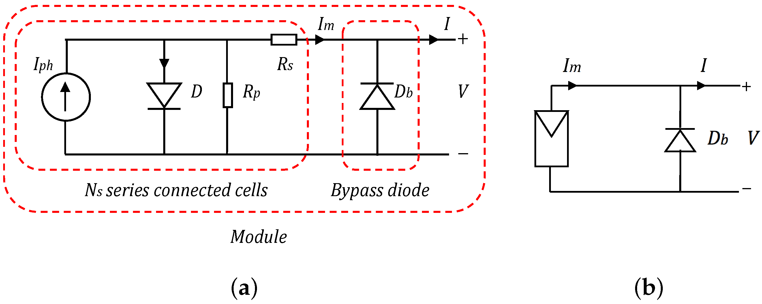
Figure 1a shows the circuit of a PV submodule formed by a group of PV cells in series connection with a protection diode (bypass diode) connected in antiparallel. A simplified representation of the PV submodule is shown in
Figure 1b, such a representation is used to ease the details of the procedure described in
Section 2.
In the circuit of
Figure 1a, the current source represents the generated current due to the photovoltaic effect, which mostly depends on the irradiance; the diode represents the non-linear behavior of the P-N junctions of the cells,
and
represent the losses due to the connections between cells and the losses by parasitic currents and other phenomena associated to the cells operation. The circuit is completed by a bypass diode, external to the submodule, which becomes active when the submodule operates under mismatching conditions.
From the circuit of
Figure 1a and using the Kirchhoff current laws, it is possible to define the relationship between the voltage (
V) and current (
I) in the submodule given by (
1), where
is the inverse saturation current of diode D,
is the ideality factor of diode D,
is the thermal voltage of diode D and
is the current flowing through the bypass diode. Additionally,
is defined as
, where
k is the Boltzmann constant,
q is the electron charge, and
T is the cells temperature in Kelvin.
The bypass diode current is given by (
2), where
and
are the inverse saturation current and the ideality factor, respectively. The bypass diode thermal voltage is defined as
, where
is temperature of the bypass diode in Kelvin. In this paper, for the sake of simplicity, it is assumed that the temperature of the cells and the temperature of the bypass diode is the same (i.e.,
), this taking into account that both the submodule and bypass diode temperatures can be considered similar if the PV module does not experiment fast irradiance changes [
31].
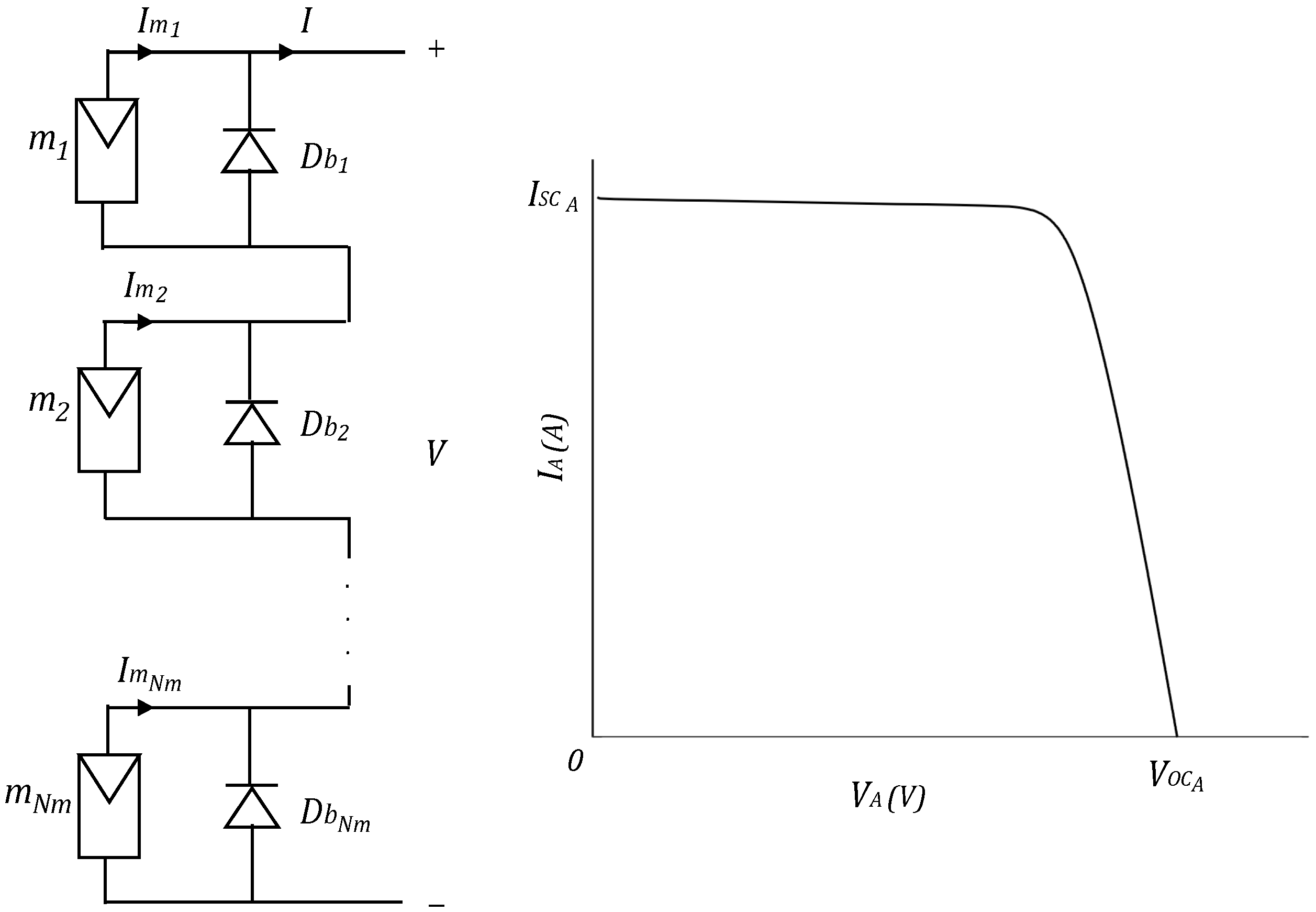
A PV module is formed by one or more submodules connected in series in a single physical structure with two terminals; hence, the terminals of each submodule and the bypass diodes are not accessible without opening the junction box. Moreover, the modules are typically formed by three submodules [
32,
33,
34,
35], however, it is also possible to find modules with one [
36], two [
37] and four [
38] submodules. As example,
Figure 2 shows the structure of a PV module formed by three submodules. In such a module, the current flowing through the submodules (
I) is the same, which in turn is the module output current. That condition is valid only if the submodules operate at the same irradiance level and temperature. If the operating conditions are different (i.e., partial shading), the bypass diode associated to the shaded submodule becomes active if
I is greater than the short-circuit current (
) of the submodule.
3. Procedure for Estimating the Bypass Diode Parameters
This section is devoted to introduce the proposed solution for estimating the bypass diode parameters of a PV module. In the proposed procedure the following restrictions were considered: (i) the procedure allows to calculate the parameters of one bypass diode at time, (ii) the module is formed by two submodules at least or, if the module is formed by one submodule, there are at least two modules, (iii) the parameters of the cells are considered the same for the sake of simplicity and (iv) the measured I-V curves (curve A and curve B) must be taken in a short time to ensure the same irradiance and temperature conditions of the submodules.
The first step is to define the number of submodules (
) in the module. Then, an I-V curve with all submodules in the module operating at uniform conditions is obtained, such a curve is named as curve A and it is obtained by performing a current sweep, i.e., from
to
increasing the current with fixed steps of
. Then, vectors
and
(with
) are obtained, where
N corresponds to the number of points in the I-V curve.
Figure 3 shows structure and the curve A of a PV module formed by
submodules under uniform conditions.
After obtaining the curve A, the submodule, whose bypass diode model parameters needs to be estimated, must be fully covered to perform the same current sweep (
N points), as in previous step, to obtain vectors
and
of a new I-V curve, which is named as curve B. When a submodule is fully shaded, its photovoltaic current (
) is approximately
[A], therefore in such a submodule the current flows through its bypass diode. As it was previously explained, such a current is the same current flowing through the module due to the series connection of the submodules (
). Therefore, the voltage of curve B can be related with the voltage of curve A by using (
3), where the factor
represents the voltage of the unshaded submodules and
is the voltage of the bypass diode, which is active in the shaded submodule. Moreover, using the exponential model of the bypass diode it is possible to define
as shown in (4).
To illustrate the procedure,
Figure 4 shows the circuital model of a PV module with the submodule
completely covered, to estimate its parameters, as well as the module I-V curve (curve B). Moreover,
Figure 4 shows that the current provided by submodule
is approximately zero (
[A]), hence, the module current (
I) flows through the bypass diode
, which means that the current of the curve B is the current of the bypass diode
. In general, to estimate that parameters of submodule
, such a submodule must be fully covered (i.e.,
[A]) to measure curve B after measuring curve A.
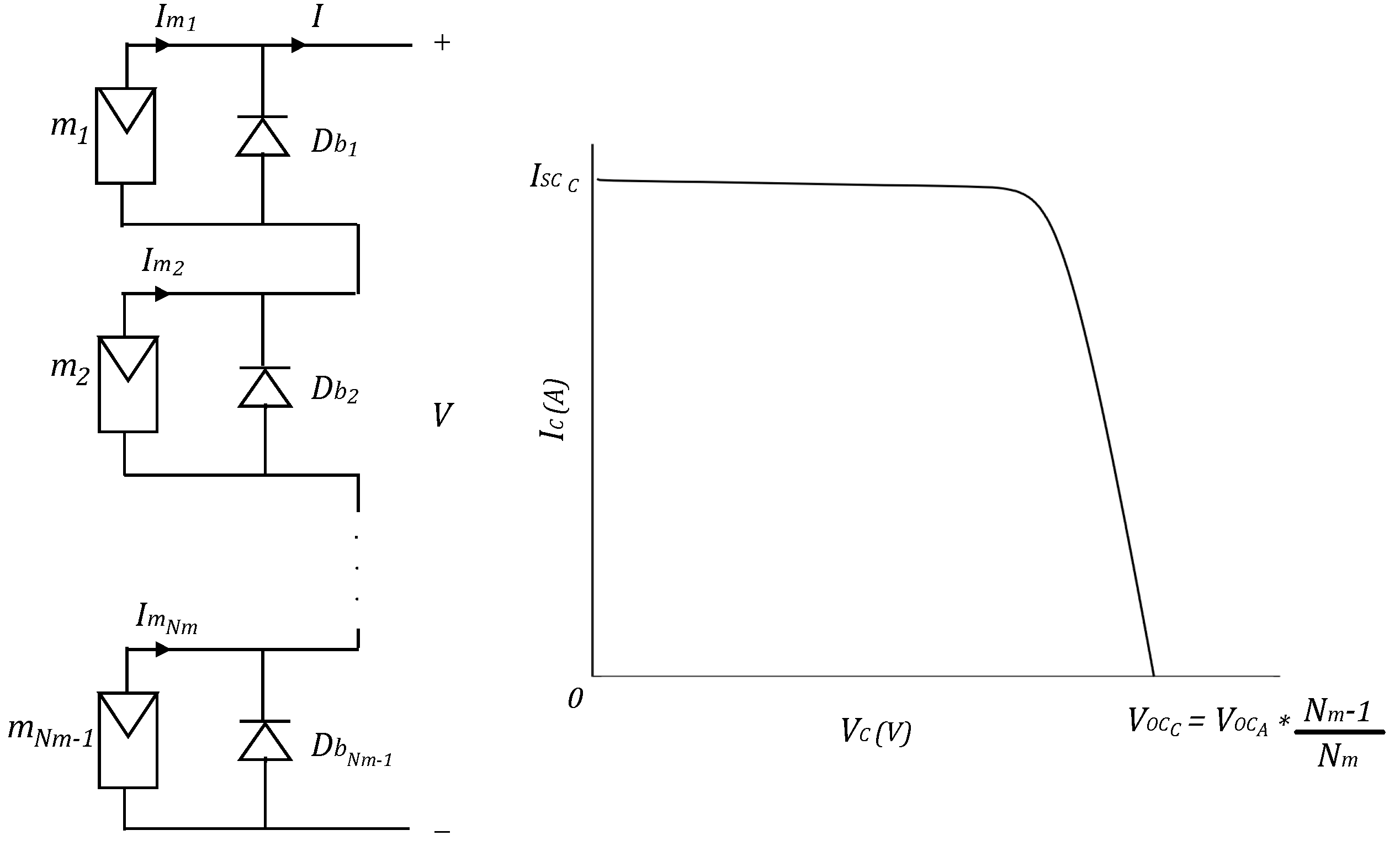
After obtaining curves A and B, the module I-V curve without the shaded submodule (i.e., I-V curve of
unshaded submodules) must be estimated, such a curve is named as curve C. The current values of curve C (
) are assumed equal to the values of curve A, as shown in (
5), because the current in a module does not depend on the number of active submodules but the area of its cells [
39]. The voltage values of curve C (
) can be calculated by scaling the voltages of curve A in proportion to the number of unshaded submodules, as it is shown in (
3). The circuital model of a module with
active submodules and its I-V curve are presented in
Figure 5, while (
5) and (
6) are the expressions of the current and voltage vectors of curve C.
By comparing the circuital model of a shaded submodule (
Figure 4) and the model of the module with
unshaded submodules (
Figure 5), it is observed that the difference between them is the activation of the bypass diode in the shaded submodule. Such a bypass diode provokes a voltage drop in curve B with respect to curve C, as it is shown in
Figure 6. Therefore, by subtracting the voltages of curve B to the voltages of curve C point by point, it is possible to estimate the voltage vector of the bypass diode of the shaded submodule (
) as it is represented in (
7). Such a difference can be calculated because each point of curves B and C were measured for the same current. Additionally, from the circuital model shown in
Figure 3, the module current flows through the bypass diode of the shaded submodule; then, the current vector of the bypass diode (
) is the same one of curve B as it is defined in (
8).
With vectors
and
the I-V curve of the bypass diode is estimated. From such vectors, a couple of points are be selected to be replaced in the Schottkey equation to set the system of non-linear equations shown in (
9), where the unknowns are
and
,
and
are the voltage and current of the first point of the I-V curve, respectively, and
and
are the voltage and current of the second point of the I-V curve, respectively. Such a system of equations can be solved by using numerical methods like Newton-Raphson.
The two ordered pairs
and
are defined as it is given in (
10) and (
11). On the one hand, the point in (
10) corresponds to the bypass diode voltage and current, respectively, where the current of curve B is
of its maximum power point current (
) and
represents the index of
in
. This criteria is selected because in a practical application of the proposed method it is possible that the short-circuit currents of curve A (
) and curve B (
) are not exactly the same, due to small variations in the irradiance when both curves are measured. Those variations produces a wrong estimation of the bypass diode voltages for currents close to
or
; therefore, defining the point
for currents less than
avoids errors in the estimation of
and
. On the other hand, (
11) corresponds to the point approximately in the middle of curve B, where
represents the ceiling function of
and
N is the number of points in curve B.
Finally, to calculate the parameters of the bypass diode connected to another submodule in module, such a submodule must be fully shaded and the procedure described in this section must be repeated. Therefore, by introducing a complete shadow (i.e., making
) and applying the proposed procedure at each submodule in the module, all the bypass diodes in the module can be characterized. The proposed procedure is summarize in the flowchart presented in
Figure 7.
4. Simulation Validation
The proposed procedure was implemented in a Matlab script and it was validated by means of simulations in Simulink. In the simulation tests the parameters of the Trina Solar TMS-PD05 270 W module were used, which is formed by three submodules [
40]. The bypass diode simulation parameters were extracted from the GF3045T datasheet [
41], which is a set of three bypass diodes in a single enclosure installed in the connection box of the Trina Solar TMS-PD05 270 W module. In addition, the temperature was set as 44° for both the cells and the bypass diodes because it is the normal operation temperature (NOCT) of the Trina Solar TMS-PD05 module.
Figure 8 shows the implementation of the simulation test in Simulink, in which each submodule is represented by the single-diode model. It is important to highlight that the sensors that take the measurements of current and voltages in the bypass are used in the simulation for validation purposes, however, they are not required for the proposed procedure. According the flowchart shown in
Figure 7, the I-V curves generated with Simulink were used as the “measured I-V curves A and B”, which are required to apply the proposed procedure; the estimated parameters are obtained by using (
5) to (
11). In this way, the results presented in this section are not based in Simulink mathematical functions, instead they correspond to the application of the proposed approach.
The parameters of each submodule of the Trina Solar TMS-PD05 PV module, according to the procedure proposed in [
4], are:
,
,
and
. For the simulations, two irradiance (
G) scenarios were considered to evaluate the accuracy of the proposed approach under two different operating conditions: 1000 W/m
2 and 500 W/m
2. The I-V curves of the PV submodules change significantly from one irradiance level to the other, which means that different values of
will be used as presented in
Table 1. Moreover, there is also a significant variation of the submodules model parameters (
,
,
and
) [
42], this means that different sets of parameters were calculated [
43]. Instead, the bypass diode parameters do not depend on the irradiance level. Therefore, evaluating the proposed method, for those very different irradiance conditions, enable to test the method accuracy, since the I-V data used to estimate the parameters are different for each case.
The parameters of the bypass diode used in the simulations were calculated by selecting two pairs of points from the forward-current vs. forward-voltage curve at 25 °C available in the diodes’ datasheet [
41]:
A,
V and
A,
V. The ordered pairs
and
were used to pose the system of equations defined in (
9), which was solved by using the
fsolve function of Matlab to obtain the reference values for inverse saturation current (
) and the ideality factor (
):
μA and
. Since in actual applications the diodes constructed from the same silicon sample have different parameters (sometimes with wide variations) [
44], the parameters of the three bypass diodes were defined different with the aim of making a more realistic test. Hence, the parameters of the three bypass diodes were defined as follows:
and
for submodule 1,
and
for submodule 2 and
and
for submodule 3. In this way, it is evaluated if the proposed procedure is able to estimate the bypass diodes of the three submodules if they are not the same.
4.1. Scenario 1: High Irradiance Level
The first scenario considers the irradiance
G is 1000 W/m
2. In this example, the procedure described in the previous section is used to estimate the parameters of one of the bypass diodes of the PV module. The number of submodules is defined as
, since the module is formed by 3 submodules, and the step for the current sweep is defined as
mA.
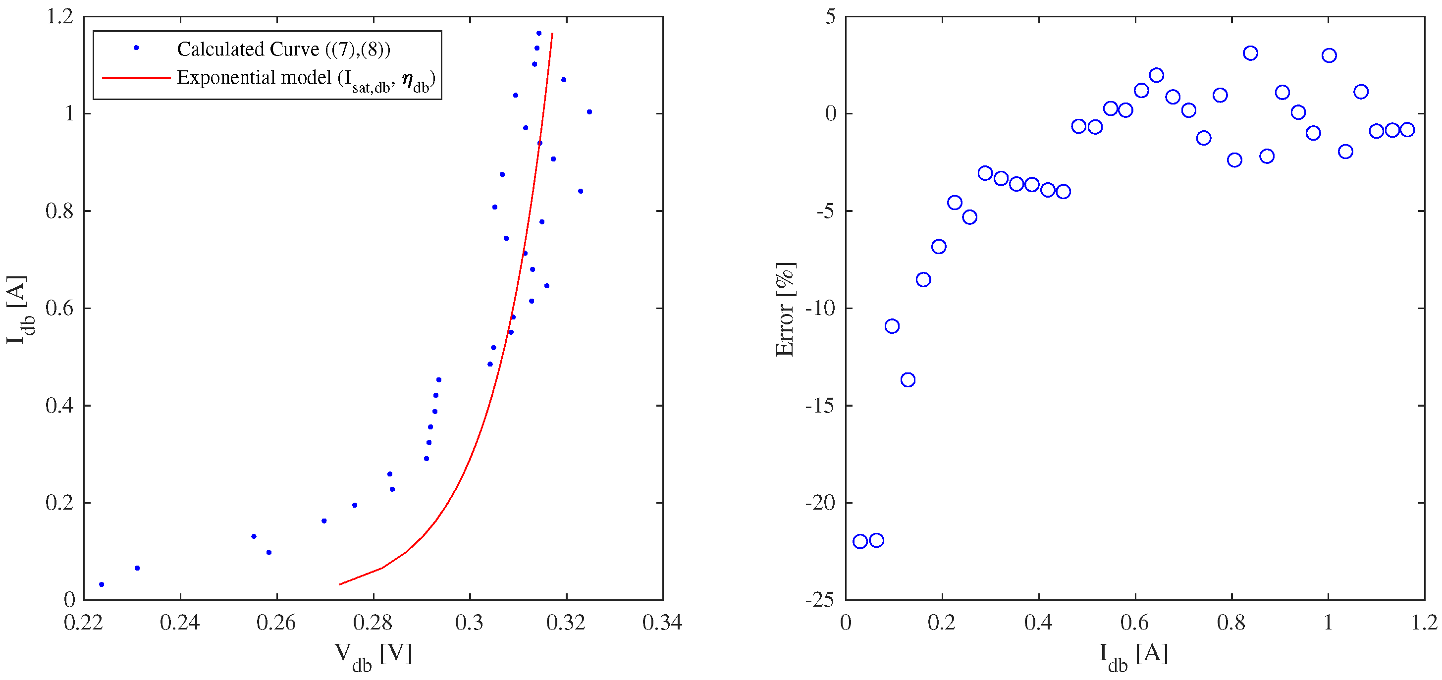
Figure 9 shows the I-V curve obtained by performing the current sweep with uniform irradiance (curve A). A new current sweep is performed this time with one of the submodules (submodule number 3) completely shaded (
A); then, the curve B is obtained. Finally, by using (
5) and (
6), the curve C is estimated.
Following the procedure described in the flowchart, the current and voltage vectors of the bypass diode connected to submodule 3 are calculated; finally the estimated inverse saturation current and the ideality factor are
μA and
.
Figure 10 shows the comparison between the I-V curves of the bypass diode obtained by using simulation and by using the proposed procedure.
In the same way, the procedure is applied to the submodules 2 and 3 to characterize all the bypass diodes in the PV module. The calculated parameters and their percentage errors with respect to the reference values are presented in
Table 2.
In order to compare the bypass diodes curves point by point, the root mean square error (RMSE) was calculated. It is worth noting that the RMSE is evaluated for the bypass diode voltages, since the currents are measured experimentally.
Table 3 presents the results, in which the reference values correspond to the Simulink results, the second column shows the errors of the bypass diodes I-V curves estimated with (
7) and (
8), and the third column contains the errors obtained with the exponential model using the parameters estimated with the proposed procedure. It can be seen how the proposed procedure introduces errors lower than 0.60 mV, which confirms the accuracy of the proposed solution.
4.2. Scenario 2: Medium Irradiance Level
In this scenario, the submodules of the PV module were exposed to a medium level of irradiance (
G = 500 W/m
2), which provokes a reduction in the photovoltaic currents as it is presented in
Table 1. The reference values used in this scenario were the same as in the previous sub section. The estimated parameters of the bypass diodes obtained by applying the proposed procedure are presented in
Table 4.
Unlike the results obtained in the scenario 1, in this case for high reference values, the error in the estimated parameters is not lower. The errors in this test oscillate between 1.82% and 2.02% for and between 0.16% and 0.17% for , which are higher than the ones obtained in the scenario 1. This increment in the error may be due to the fact that in scenario 2 the maximum bypass diodes currents is lower than the value in the scenario 1. Therefore, for scenario 2, the I-V curves cover only a part of the I-V curves for the scenario 1.
As in the previous test, the RMSE is used in order to compare the circuital simulation curve with the curve obtained by using (
7) and (
8), and the curve calculated with the exponential model and the estimated parameters (see
Table 5). In this case, the curve obtained by using (
7) and (
8) introduced an errors lower than 6.84 μV while the curves obtained with the estimated parameters introduced errors lower than 1.05 mV. Results in this section show that the proposed procedure exhibits errors different than zero in the estimation of the bypass diode parameters, even under a simulation scenario without element tolerances and measuring noise and errors. Therefore, it is expected that the errors in the experimental validation will be higher due to the measurement errors, noise and small variations in the operating conditions during the measurement of curves A and B.
5. Experimental Validation
The proposed method was validated through experimental tests using the platform shown in
Figure 11. Such a platform was formed by one Trina Solar TMS-PD05 270 W PV module composed by three submodules, a programmable electronic load BK Precision 8500 [
45], a computer with Matlab and a piece of wood to cover the submodule in which the parameters need to be estimated. The platform is placed in a building roof and it is connected to the electronic load, which in turn is connected to a computer through serial communication, this allowing to obtain the data of the I-V curves. Finally, the experimental tests were carried out in a short time in order to avoid sudden changes in the irradiance level, which allows to consider that both submodule and bypass diode temperatures are the same [
31].
The parameters of the three bypass diodes of the module where estimated using the solution introduced in this paper for high, medium and low irradiance levels, which are naturally obtained at different hours of the day and depending on the cloudiness conditions. In this way, for high irradiance short-circuit currents are , for medium irradiance levels are and for low irradiance levels . All the tests consider , therefore is defined as , where is the value of the short-circuit current of the curve A in each experimental test.
As explained in
Section 3, curves A and B correspond to the PV module; however, in the experimental platform, the module is connected to the electronic load through a pair of AWG-12 cables whose resistance (
) is different than zero (
), considering that each cable is 30 m long. Therefore, the voltages of curves A and B at the terminals of the PV module are calculated by using (
12) and (
13), where
and
are the voltages measured by the electronic load. The currents of curves A (
) and B (
) correspond to the measurements performed by the electronic load, since the current flowing through the module and the load is the same.
Figure 12 shows an example of the experimental curves A and B obtained for submodule 1, with the module exposed to high, medium and low irradiance levels, as well as the curves C obtained by applying the proposed procedure. From each pair of curves B and C in
Figure 12, the I-V curve of the bypass diode in submodule 1 is obtained and a set of bypass diode parameters is estimated by applying the proposed method. As example,
Figure 13,
Figure 14 and
Figure 15 show the show the comparison between the I-V curves of the bypass diode obtained with the proposed procedure and the ones obtained experimentally. Those figures also illustrate the percentage error of the of bypass diode voltage calculated with the estimated parameters with respect to the curve calculated with (
7) and (
8).
Ten experiments were performed for submodule 1 for each irradiance level in order to illustrate the behavior of the estimated bypass diode parameters with the proposed method.
Table 6 shows the average values and standard deviations of
and
for each irradiance level, as well as the RMSE in the reproduction of the bypass diode I-V. Moreover,
Table 7 introduces the average values and standard deviations of
,
and
.
It can be observed that is significantly reduced when the irradiance decreases and the standard deviation is in the same order of the estimated values (i.e., relatively high). Although, is also reduced with irradiance reductions, its standard deviation is low with respect to the average values. Moreover, the errors in the I-V reproduction are in the order of mV with a relatively high standard deviations which shows that the proposed procedure is able to reproduce the electrical behavior of the bypass diode under different irradiance levels but I-V reproduction accuracy depends on the irradiance and temperature conditions.
It is worth noting that the experimental platform is outdoors, therefore, it is difficult to obtain two set of curves A and B for the module operating under the same conditions. Such variability in the irradiance and temperature conditions is one of the reasons of the variability of the bypass diode parameters and I-V curve reproduction errors. The variability in the operating conditions is illustrated by
Table 7, which shows standard deviations in the module temperature close to 3 K and in the short-circuit current (proportional to the irradiance) of hundreds of mA.
In the same way, the proposed procedure was applied to submodules 2 and 3 to calculate the parameters of their bypass diodes for ten experiments for each irradiance level.
Table 8 and
Table 9 present the estimated parameters with their respective RMSE in the reproduction of the bypass diodes I-V curves for each irradiance condition; while
Table 10 and
Table 11 introduce the information of thermal voltage, module temperature and short-circuit currents for the different experiments.
In general, the average and standard deviation of the bypass diodes’ parameters are the same as the ones introduced for submodule 1 in
Table 6 and
Table 7, with the reduction of the magnitude in the parameters for lower irradiance levels and high standard deviations for
and low standard deviations for
. Nonetheless, it is worth noting that the smallest value of
for submodule 2 is obtained for medium irradiance and not for low irradiance as for the other modules. Finally, the errors in the reproductions of the I-V curves are similar for the three submodules.
The results show that the proposed procedure allows to calculate the parameters to reproduce the electrical behavior of the bypass diodes in a PV module with RMSE values lower than 31.15 mV. Considering that there is no other work reported in literature addressing the estimation of the diode parameters present in the Trina Solar PV module used in this paper, it is difficult to qualify the obtained errors as low or high. However, for contrasting purposes, the values given in works [
46,
47] include diode inverse-saturation currents between 2 μA [
46] and 10 ηA [
47] and ideality factors between 2 [
46] and 3.4 [
47] for any irradiance condition. Hence,
values used in [
46,
47] may be three or six order of magnitude lower than the ones obtained in this paper, for high irradiances, and three or six orders of magnitude higher than the values obtained for low irradiances. Moreover,
values used in [
46,
47] are close to the ones obtained in the proposed method for high irradiances, but estimated
values may be one order of magnitude lower than the ones used in [
46,
47] for medium and low irradiances. Therefore, if the parameter values reported in [
46,
47] are considered for any operation condition, the error in the reproduction of the bypass diodes I-V curves may increase, causing issues in the reproduction of the I-V curves in a PV generator.
The proposed procedure can be used to monitor the state of all bypass diodes in a module by performing a sequential estimation of each diode parameters. Such a complete information of all bypass diodes can be used for diagnostic purposes, or for any application that requires the mathematical model of the bypass diodes to reproduce the electrical behavior of PV generators operating under mismatching conditions. This could be an improvement for models of PV arrays that assume equal the parameters of all the bypass diodes even under different irradiance conditions [
6,
12,
46,
47].
6. Conclusions
In this paper, a non-invasive procedure to estimate the parameters and of the exponential model, used to reproduce the behavior of the bypass diodes in a PV module, was introduced. The procedure is based on the relationships between the I-V curves of the module with and without shading. Since the proposed procedure is based on the acquisition of voltage and current data of the PV module, it is a non-invasive method; therefore, there is no need of disconnecting the bypass diode of the module. In addition, the steps required by the proposed method have low complexity since only two current sweeps (with and without shading) are required and there is no need to identify the model parameters of the PV submodules that form the module.
The proposed procedure was validated using simulation (Simulink) and experimental results for a PV module formed by three submodules. In the simulations, the parameters of all bypass diode were considered different and the proposed procedure was evaluated for high (1000 W/m2) and medium (500 W/m2) irradiance scenarios. The errors in the parameters estimation were lower than 2.02% and 0.17% for and , respectively; while the RMSE in the reproduction of the bypass diodes I-V curves were lower than 1.05 mV for both scenarios.
For the experimental validation, the proposed method was applied to estimate the bypass diode parameters for a PV module formed by three submodules. The parameters of the three bypass diodes were estimated for high, medium and low irradiance levels, taking around ten experiments for each condition. The RMSE of the I-V curves reproduction were lower than 31.15 mV and the results show that the magnitudes of the estimated parameters are reduced when the irradiance is reduced. Moreover, the average and standard deviation values of and suggest that it would be necessary to consider other models for representing the bypass diode under any irradiance conditions, otherwise the exponential model parameters must be adjusted if more accuracy is required.
Although the proposed method cannot be applied by using the I-V tracers available in the market, due to their low voltage measurement accuracy, it is an interesting future work to develop a portable electronic device able to implement the proposed procedure to complement the information obtained with the I-V tracers. In addition, the authors are currently working in a procedure in which it is not necessary to totally cover a submodule to estimate its parameters; instead the idea is to take advantage of the partial shading conditions produced in the submodule and the activation and deactivation of a bypass diode to estimate its parameters. In the same way, the next stage of this work considers to represent the bypass diodes through other circuital models in order to reduce the errors in the reproduction of the electrical behavior of the bypass diodes for medium and high irradiance conditions.

 ,
, 


