
Machine-Learning-Assisted Instantaneous Frequency Measurement Method Based on Thin-Film Lithium Niobate on an Insulator Phase Modulator for Radar Detection

Abstract
:1. Introduction
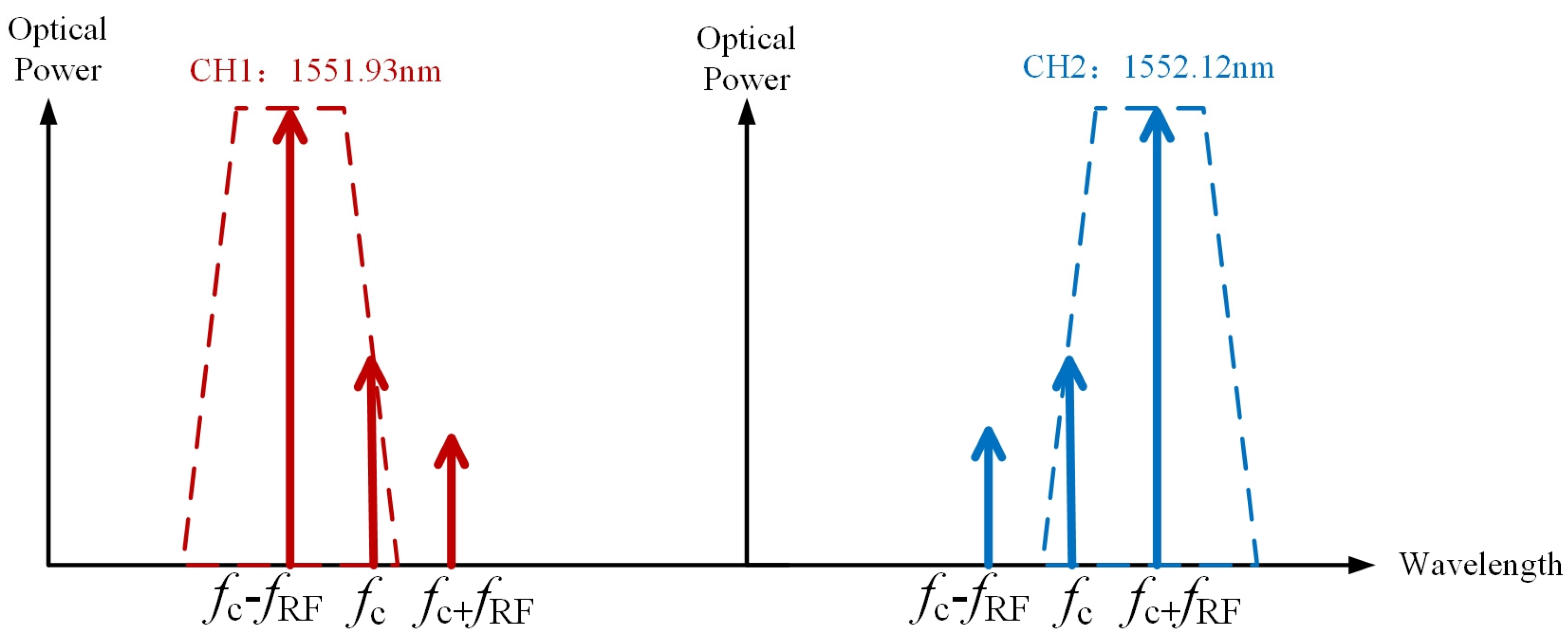
- The measurement system consists of an LNOI phase modulator and a wavelength division multiplexer (WDM) without the need for bias point control, with a simple and reliable architecture and a high degree of integration.
- LNOI phase modulators with low half-wave voltages provide higher sensitivity to the system and, in the future, will enable ultra-high-modulation bandwidths, further extending the measurement range.
- The tunability of carrier wavelength and filtering range can flexibly change the measurement range and measurement accuracy of the system to adapt to a wider range of scenarios.
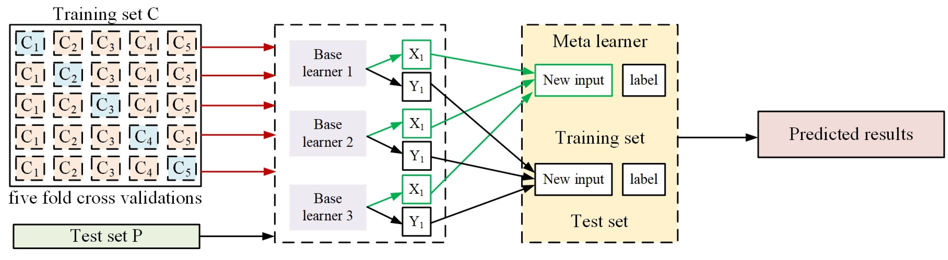
- The use of stacked integrated learning models can further improve the system measurement’s accuracy and stability.
2. Theoretical Analysis
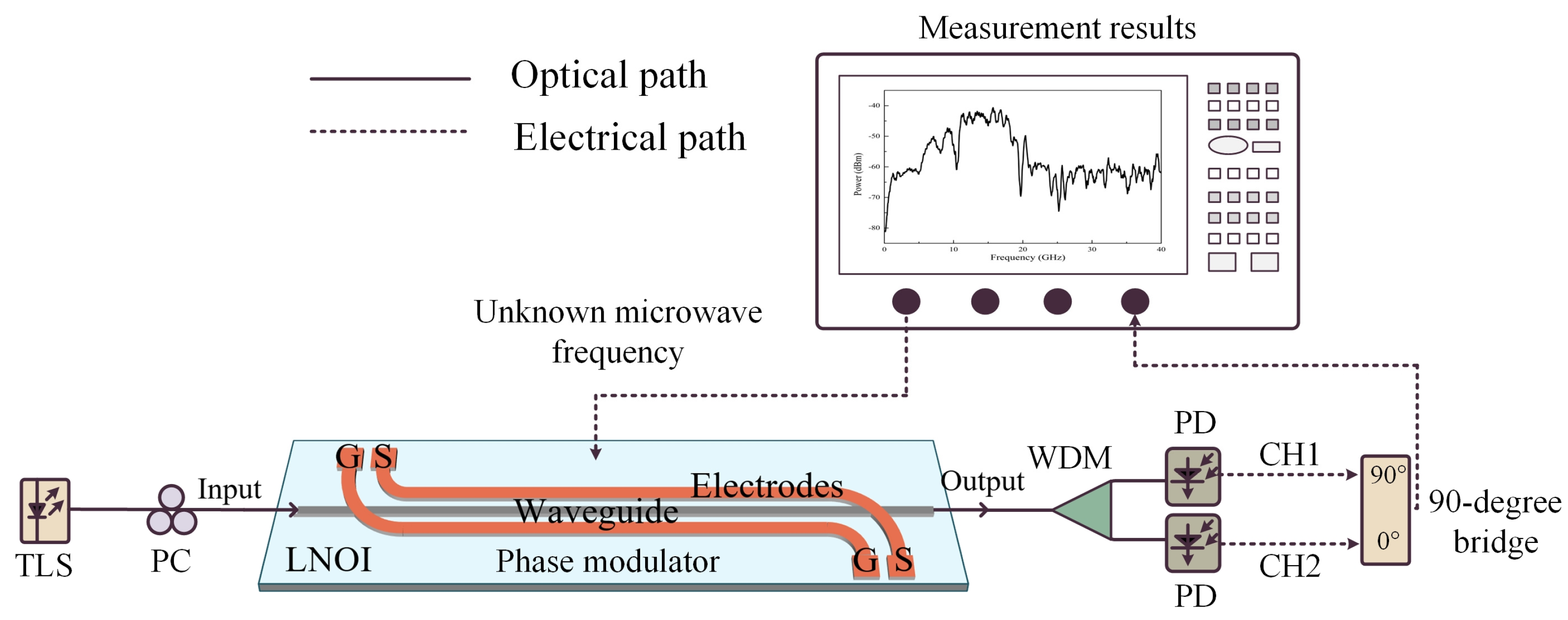
2.1. MWP IFM System Architecture and Principle
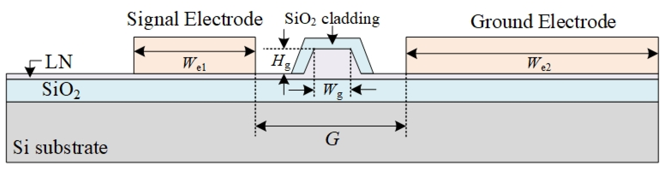
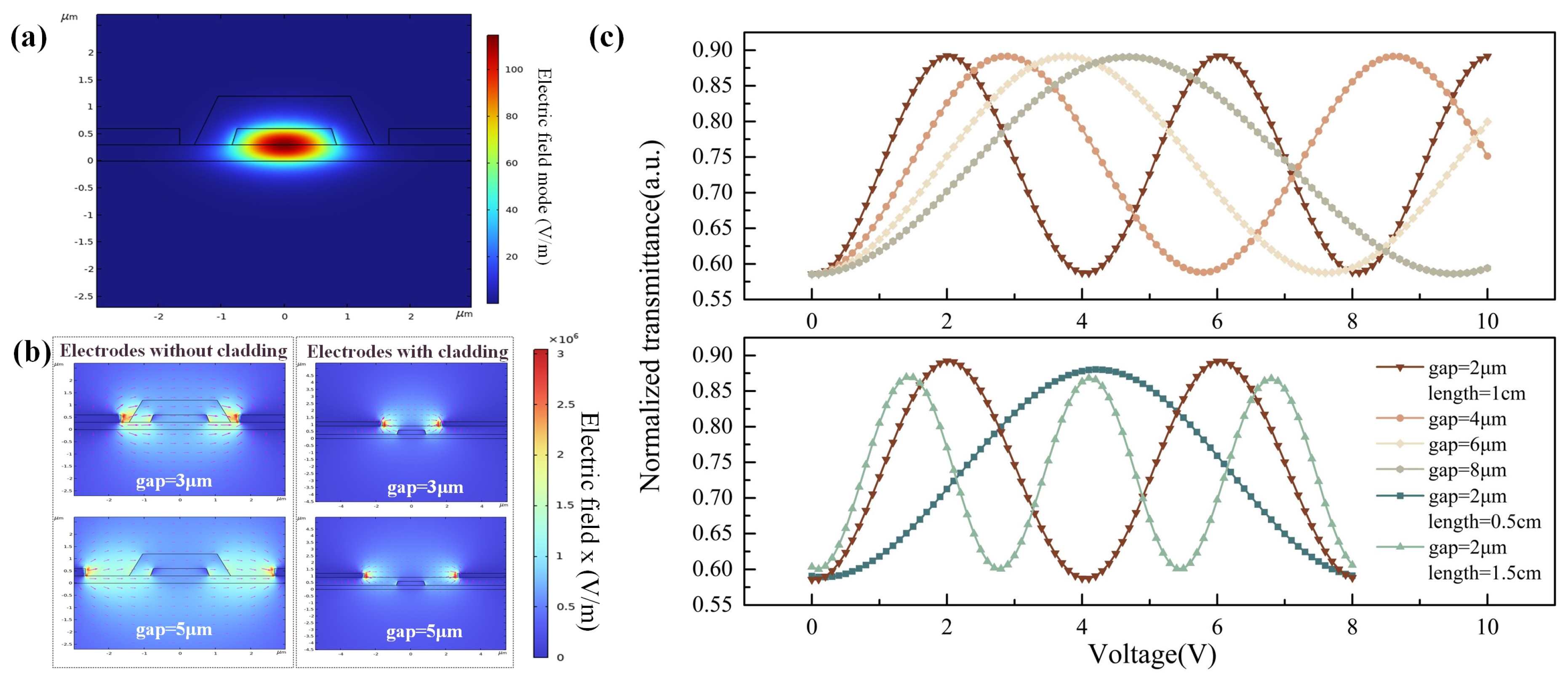
2.2. Design of Low-Voltage LNOI Phase Modulator
3. Results
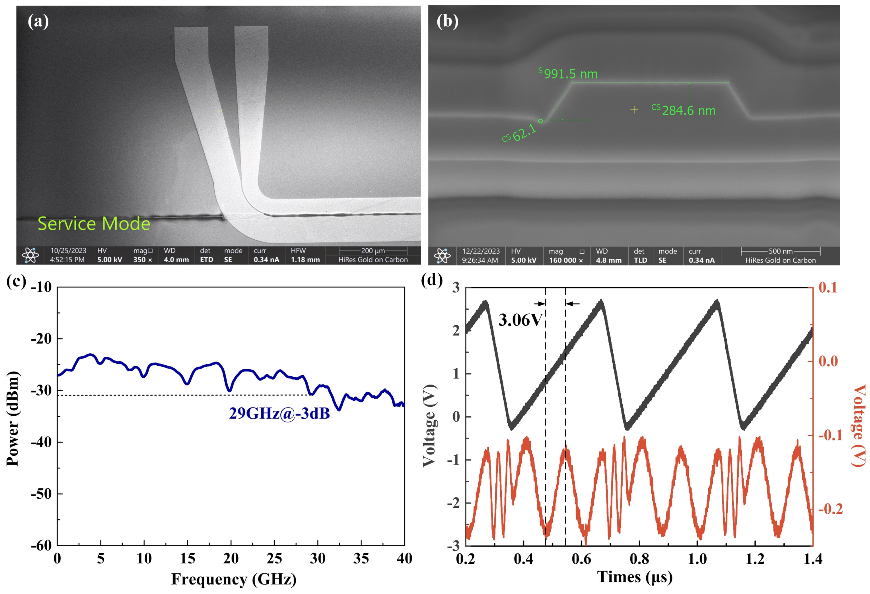
3.1. Preparation and Characterization of LNOI Phase Modulator
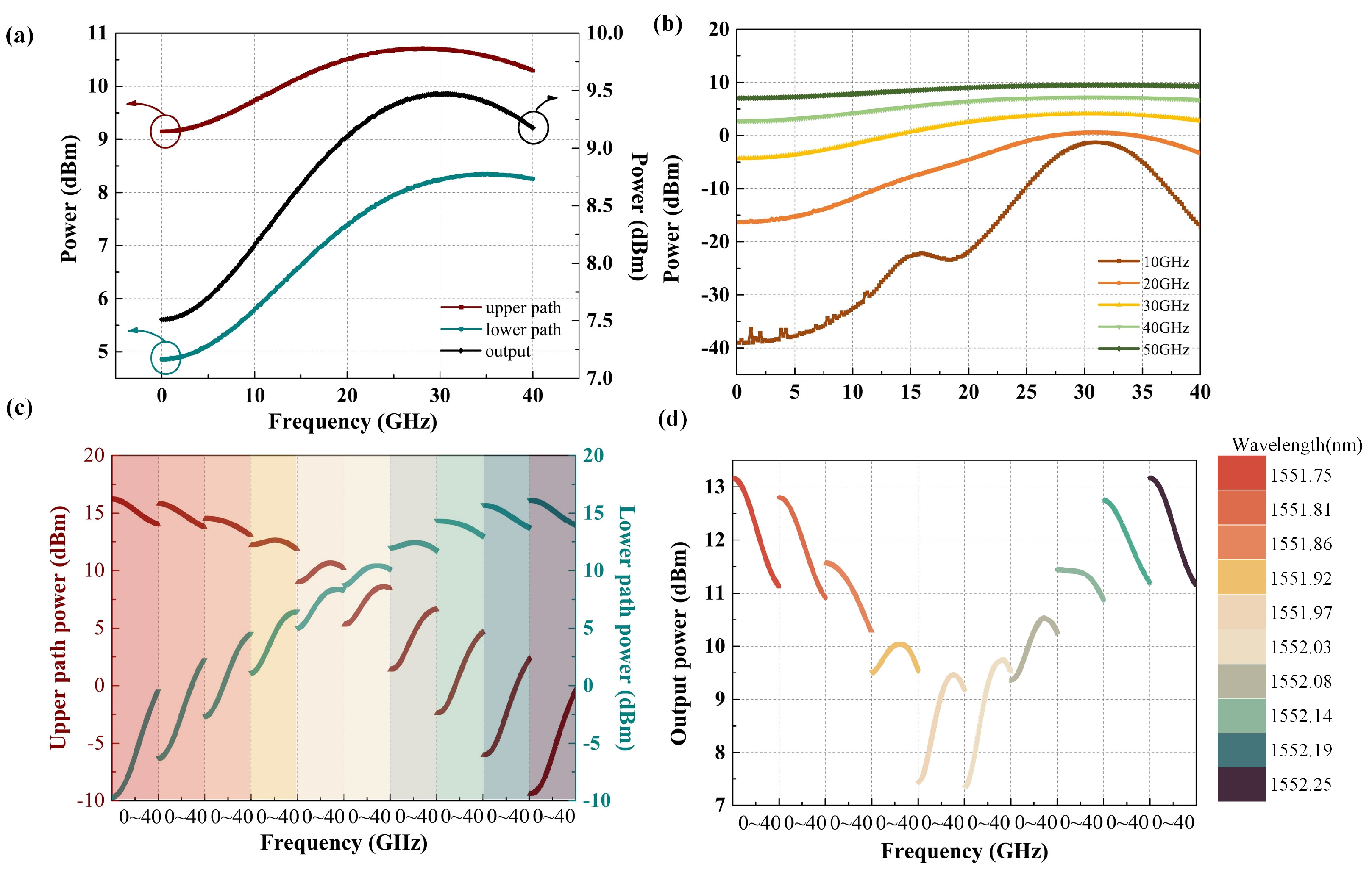
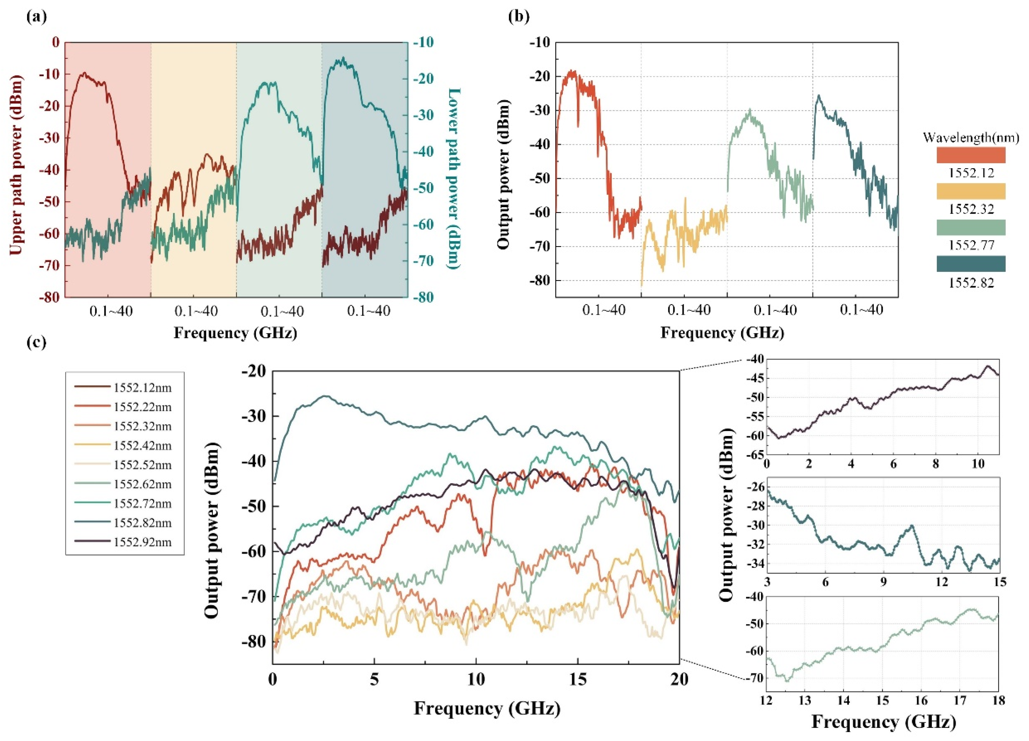
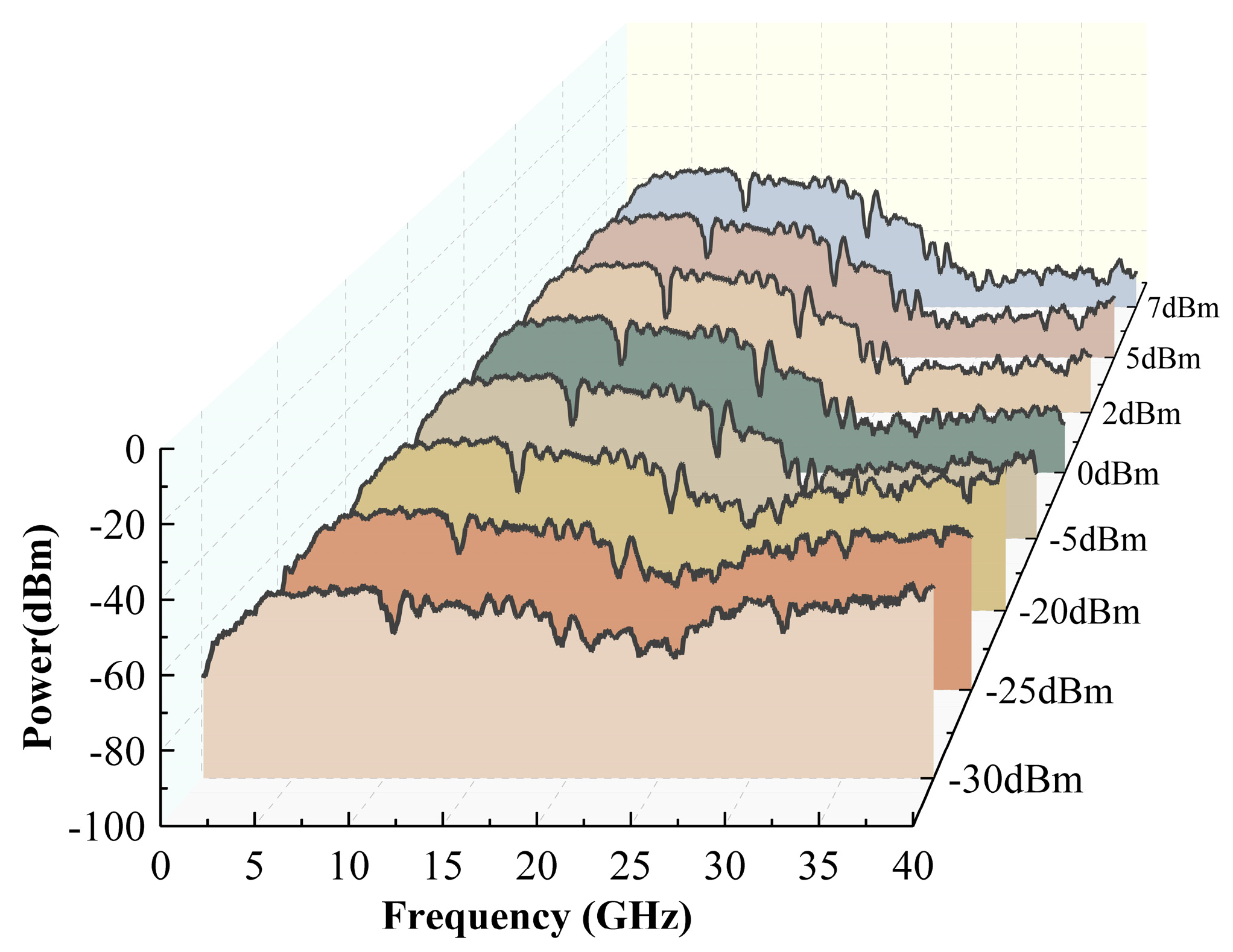
3.2. Instantaneous Frequency Measurement and Optimization
4. Discussion
5. Conclusions
Author Contributions
Funding
Institutional Review Board Statement
Informed Consent Statement
Data Availability Statement
Conflicts of Interest
Appendix A

| Input Signal (Hz) | Output Signal (Hz) | Measurement Error Percentage | Input Signal (Hz) | Output Signal (Hz) | Measurement Error Percentage |
|---|---|---|---|---|---|
| 10,025,100,000 | 10,023,736,586 | 0.01% | 7,381,750,000 | 7,321,957,825 | 0.81% |
| 5,586,250,000 | 5,579,099,600 | 0.13% | 8,429,130,000 | 8,388,670,176 | 0.48% |
| 5,386,750,000 | 5,382,117,395 | 0.09% | 9,177,250,000 | 9,157,427,140 | 0.22% |
| 8,628,630,000 | 8,628,529,045 | 0.00% | 10,025,100,000 | 9,908,608,338 | 1.16% |
| 698,500,000 | 684,781,460 | 1.96% | 3,691,000,000 | 3,684,208,560 | 0.18% |
| 2,643,630,000 | 2,617,273,009 | 1.00% | 6,284,500,000 | 6,277,712,740 | 0.11% |
| 6,583,750,000 | 6,583,522,202 | 0.00% | 9,376,750,000 | 9,328,365,970 | 0.52% |
| 748,375,000 | 747,938,697.4 | 0.06% | 6,683,500,000 | 6,681,220,927 | 0.03% |
| 2,693,500,000 | 2,677,500,610 | 0.59% | 4,838,130,000 | 4,834,051,955 | 0.08% |
| 9,875,500,000 | 9,882,847,372 | 0.07% | 4,937,880,000 | 4,937,857,016 | 0.00% |
| 9,975,250,000 | 9,974,608,591 | 0.01% | 8,429,130,000 | 8,413,030,362 | 0.19% |
| 7,531,380,000 | 7,463,974,149 | 0.90% | 2,045,130,000 | 2,041,775,987 | 0.16% |
| 2,444,130,000 | 2,437,481,966 | 0.27% | 3,591,250,000 | 3,551,530,775 | 1.11% |
| 5,536,380,000 | 5,521,963,266 | 0.26% | 7,381,750,000 | 7,377,151,170 | 0.06% |
| 3,890,500,000 | 3,866,106,565 | 0.63% | 4,439,130,000 | 4,438,810,383 | 0.01% |
| 3,591,250,000 | 3,581,661,363 | 0.27% | 3,192,250,000 | 3,191,835,008 | 0.01% |
| 299,500,000 | 297,921,635 | 0.53% | 6,583,750,000 | 6,578,575,396 | 0.08% |
| 7,331,880,000 | 7,331,672,508 | 0.00% | 4,489,000,000 | 4,317,520,200 | 3.82% |
| 2,494,000,000 | 2,502,030,680 | 0.32% | 3,691,000,000 | 3,547,863,020 | 3.88% |
| 9,127,380,000 | 9,219,110,169 | 1.01% | 6,234,630,000 | 6,205,950,702 | 0.46% |
| 8,229,630,000 | 8,379,656,155 | 1.82% | 3,591,250,000 | 3,590,136,713 | 0.03% |
| 2,543,880,000 | 2,564,688,938 | 0.82% | 7,681,000,000 | 7,678,020,747 | 0.04% |
| 7,730,880,000 | 7,738,343,152 | 0.10% | 9,626,130,000 | 9,597,636,655 | 0.30% |
| 3,192,250,000 | 3,171,723,833 | 0.64% | 9,127,380,000 | 9,108,851,419 | 0.20% |
| 2,344,380,000 | 2,257,989,597 | 3.69% | 4,489,000,000 | 4,465,073,630 | 0.53% |
| 5,885,500,000 | 5,833,060,195 | 0.89% | 7,481,500,000 | 7,488,173,498 | 0.09% |
| 7,331,880,000 | 7,331,617,519 | 0.00% | 9,426,630,000 | 9,440,392,880 | 0.15% |
| 9,875,500,000 | 9,871,508,619 | 0.04% | 8,878,000,000 | 8,930,824,100 | 0.60% |
| 3,142,380,000 | 3,133,644,184 | 0.28% | 4,638,630,000 | 4,655,329,068 | 0.36% |
| 2,593,750,000 | 2,593,573,625 | 0.01% | 3,341,880,000 | 3,346,346,810 | 0.13% |
| 8,479,000,000 | 8,543,779,560 | 0.76% | 6,434,130,000 | 6,421,326,081 | 0.20% |
| 4,987,750,000 | 5,001,266,803 | 0.27% | 3,990,250,000 | 3,990,018,566 | 0.01% |
| 3,940,380,000 | 3,971,193,772 | 0.78% | 7,531,380,000 | 7,531,003,431 | 0.01% |
| 5,985,250,000 | 5,988,676,502 | 0.06% | 5,486,500,000 | 5,486,009,507 | 0.01% |
| 9,326,880,000 | 9,352,435,651 | 0.27% | 6,234,630,000 | 6,228,038,126 | 0.11% |
| 7,681,000,000 | 7,604,420,430 | 1.00% | 2,244,630,000 | 2,244,374,786 | 0.01% |
| 8,828,130,000 | 8,776,838,565 | 0.58% | 8,329,380,000 | 8,316,611,060 | 0.15% |
| 6,533,880,000 | 6,493,173,928 | 0.62% | 9,925,380,000 | 9,809,848,577 | 1.16% |
| 499,000,000 | 494,284,450 | 0.95% | 6,234,630,000 | 6,224,841,631 | 0.16% |
| 8,179,750,000 | 8,162,572,525 | 0.21% | 6,783,250,000 | 6,910,368,105 | 1.87% |
| Input Signal (Hz) | Output Signal (Hz) | Measurement Error Percentage | Input Signal (Hz) | Output Signal (Hz) | Measurement Error Percentage |
|---|---|---|---|---|---|
| 9,324,750,000 | 9,366,804,622.5 | 0.45% | 13,313,700,000 | 13,399,972,776 | 0.65% |
| 8,474,870,000 | 8,550,804,835.2 | 0.90% | 9,381,370,000 | 9,404,729,611.30 | 0.25% |
| 13,386,100,000 | 13,472,306,484 | 0.64% | 7,771,020,000 | 7,779,490,411.80 | 0.11% |
| 9,593,860,000 | 9,634,058,273.4 | 0.42% | 9,200,200,000 | 9,230,008,648.00 | 0.32% |
| 13,178,400,000 | 13,256,811,480 | 0.60% | 9,193,210,000 | 9,279,993,902.40 | 0.94% |
| 5,019,690,000 | 5,039,618,169.30 | 0.40% | 14,254,700,000 | 14,242,583,505 | 0.09% |
| 4,309,780,000 | 4,346,887,205.80 | 0.86% | 14,267,700,000 | 14,185,375,371 | 0.58% |
| 10,957,900,000 | 10,971,268,638 | 0.12% | 10,714,700,000 | 10,636,482,690 | 0.73% |
| 8,049,770,000 | 8,125,518,335.7 | 0.94% | 4,105,320,000 | 4,081,057,558.80 | 0.59% |
| 9,046,170,000 | 9,108,588,573 | 0.69% | 7,778,310,000 | 7,754,430,588.30 | 0.31% |
| 9,978,090,000 | 10,001,738,073.3 | 0.24% | 5,973,280,000 | 5,966,291,262.40 | 0.12% |
| 7,877,340,000 | 7,927,991,296.2 | 0.64% | 4,327,360,000 | 4,287,807,929.60 | 0.91% |
| 8,605,630,000 | 8,635,749,705 | 0.35% | 5,098,780,000 | 5,007,562,825.80 | 1.79% |
| 11,870,600,000 | 11,900,039,088 | 0.25% | 9,260,410,000 | 9,348,198,686.80 | 0.95% |
| 12,895,100,000 | 12,899,987,758.7 | 0.04% | 11,630,500,000 | 11,760,994,210 | 1.12% |
| 8,016,730,000 | 8,031,320,448.60 | 0.18% | 12,877,200,000 | 12,984,853,392 | 0.84% |
| 11,484,500,000 | 11,496,099,345 | 0.10% | 5,444,730,000 | 5,489,975,706.30 | 0.83% |
| 5,463,150,000 | 5,481,670,078.50 | 0.34% | 10,019,500,000 | 9,940,245,755.00 | 0.79% |
| 13,989,700,000 | 14,100,498,424 | 0.79% | 4,232,630,000 | 4,225,265,223.80 | 0.17% |
| 9,259,720,000 | 9,291,295,645.2 | 0.34% | 5,871,120,000 | 5,840,003,064.00 | 0.53% |
| 8,123,120,000 | 8,131,202,504.4 | 0.10% | 4,064,540,000 | 4,061,003,850.20 | 0.09% |
| 7,115,480,000 | 7,100,964,420.8 | 0.20% | 5,520,600,000 | 5,511,270,186.00 | 0.17% |
| 12,197,400,000 | 12,138,730,506 | 0.48% | 9,899,990,000 | 9,891,971,008.10 | 0.08% |
| 13,375,600,000 | 13,351,256,408 | 0.18% | 11,801,200,000 | 11,698,647,572 | 0.87% |
| 4,591,680,000 | 4,543,375,526.4 | 1.05% | 6,460,430,000 | 6,455,455,468.90 | 0.08% |
| 14,012,900,000 | 14,009,705,058.8 | 0.02% | 3,768,740,000 | 3,753,062,041.60 | 0.42% |
| 14,007,000,000 | 13,934,163,600 | 0.52% | 12,937,600,000 | 12,945,880,064 | 0.06% |
| 3,356,200,000 | 3,340,694,356 | 0.46% | 14,279,200,000 | 14,229,508,384 | 0.35% |
| 6,225,540,000 | 6,179,969,047.2 | 0.73% | 3,694,690,000 | 3,660,218,542.30 | 0.93% |
| 10,560,400,000 | 10,616,686,932 | 0.53% | 4,365,560,000 | 4,340,021,474.00 | 0.59% |
| 10,664,800,000 | 10,639,951,016 | 0.23% | 11,051,600,000 | 11,024,192,032 | 0.25% |
| 10,776,200,000 | 10,760,143,462 | 0.15% | 8,943,570,000 | 8,858,874,392.10 | 0.95% |
| 10,737,600,000 | 10,636,881,312 | 0.94% | 7,384,570,000 | 7,363,376,284.10 | 0.29% |
| 5,019,300,000 | 4,991,141,727 | 0.56% | 4,951,410,000 | 4,967,749,653.00 | 0.33% |
| 11,041,200,000 | 10,982,350,404 | 0.53% | 14,699,300,000 | 14,711,794,405 | 0.09% |
| 9,158,090,000 | 9,098,287,672.3 | 0.65% | 10,858,600,000 | 11,065,673,502 | 1.91% |
| 9,324,750,000 | 9,366,804,622.5 | 0.45% | 13,313,700,000 | 13,399,972,776 | 0.65% |
| Input Signal (Hz) | Output Signal (Hz) | Measurement Error Percentage | Input Signal (Hz) | Output Signal (Hz) | Measurement Error Percentage |
|---|---|---|---|---|---|
| 15,774,400,000 | 15,776,072,086 | 0.01% | 14,416,400,000 | 14,404,765,965 | 0.08% |
| 17,823,900,000 | 17,826,288,403 | 0.01% | 13,326,600,000 | 13,286,486,934 | 0.30% |
| 13,972,600,000 | 13,979,865,752 | 0.05% | 16,756,600,000 | 16,750,936,269 | 0.03% |
| 14,414,700,000 | 14,429,402,994 | 0.10% | 16,675,700,000 | 16,668,129,232 | 0.05% |
| 17,184,200,000 | 17,185,437,262 | 0.01% | 14,368,100,000 | 14,343,674,230 | 0.17% |
| 13,052,900,000 | 13,053,760,186 | 0.01% | 13,958,800,000 | 13,956,873,686 | 0.01% |
| 17,153,000,000 | 17,167,700,121 | 0.09% | 17,153,500,000 | 17,150,069,300 | 0.02% |
| 17,079,200,000 | 17,077,992,501 | 0.01% | 16,227,100,000 | 16,226,829,007 | 0.00% |
| 13,013,600,000 | 13,004,958,970 | 0.07% | 16,571,700,000 | 16,573,325,684 | 0.01% |
| 13,580,400,000 | 13,568,435,668 | 0.09% | 13,994,900,000 | 14,004,388,542 | 0.07% |
| 12,576,900,000 | 12,553,758,504 | 0.18% | 15,782,800,000 | 15,810,309,420 | 0.17% |
| 15,820,200,000 | 15,823,996,848 | 0.02% | 13,117,700,000 | 13,125,937,916 | 0.06% |
| 17,263,700,000 | 17,277,321,059 | 0.08% | 14,799,300,000 | 14,804,435,357 | 0.03% |
| 12,995,600,000 | 13,040,044,952 | 0.34% | 16,262,900,000 | 16,259,192,059 | 0.02% |
| 13,477,400,000 | 13,389,527,352 | 0.65% | 12,349,000,000 | 12,331,760,796 | 0.14% |
| 15,091,800,000 | 15,080,979,179 | 0.07% | 15,720,700,000 | 15,714,348,837 | 0.04% |
| 14,814,300,000 | 14,800,016,837 | 0.10% | 13,158,400,000 | 13,162,571,213 | 0.03% |
| 17,931,300,000 | 17,916,112,189 | 0.08% | 17,083,300,000 | 17,083,132,513 | 0.00% |
| 13,454,300,000 | 13,408,555,380 | 0.34% |
References
- Fandiño, J.S.; Muñoz, P.; Doménech, D.; Capmany, J. A monolithic integrated photonic microwave filter. Nat. Photonics 2017, 11, 124–129. [Google Scholar] [CrossRef]
- Marpaung, D.; Yao, J.; Capmany, J. Integrated microwave photonics. Nat. Photonics 2019, 13, 80–90. [Google Scholar] [CrossRef]
- Zhang, W.; Yao, J. A fully reconfigurable waveguide Bragg grating for programmable photonic signal processing. Nat. Commun. 2018, 9, 1396. [Google Scholar] [CrossRef] [PubMed]
- Gruchala, H.; Czyzewski, M. The instantaneous frequency measurement receiver in the complex electromagnetic environment. In Proceedings of the 15th International Conference on Microwaves, Radar and Wireless Communications (IEEE Cat. No. 04EX824), Warsaw, Poland, 17–19 May 2004; pp. 155–158. [Google Scholar]
- Capmany, J.; Novak, D. Microwave photonics combines two worlds. Nat. Photonics 2007, 1, 319. [Google Scholar] [CrossRef]
- Lin, T.; Zou, C.; Zhang, Z.; Zhao, S.; Liu, J.; Li, J.; Zhang, K.; Yu, W.; Wang, J.; Jiang, W. Differentiator-based photonic instantaneous frequency measurement for radar warning receiver. J. Light. Technol. 2020, 38, 3942–3949. [Google Scholar] [CrossRef]
- Zou, X.; Lu, B.; Pan, W.; Yan, L.; Stöhr, A.; Yao, J. Photonics for microwave measurements. Laser Photonics Rev. 2016, 10, 711–734. [Google Scholar] [CrossRef]
- Pan, S.; Yao, J. Photonics-based broadband microwave measurement. J. Light. Technol. 2017, 35, 3498–3513. [Google Scholar] [CrossRef]
- Tao, Y.; Yang, F.; Tao, Z.; Chang, L.; Shu, H.; Jin, M.; Zhou, Y.; Ge, Z.; Wang, X. Fully on-chip microwave photonic instantaneous frequency measurement system. Laser Photonics Rev. 2022, 16, 2200158. [Google Scholar] [CrossRef]
- Wang, D.; Zhang, X.; Zhou, Y.; Yang, Z.; Dong, W. Dual-functional frequency and phase measurement system based on photonics assisted Brillouin technique induced carrier processing. Opt. Laser Technol. 2023, 157, 108747. [Google Scholar] [CrossRef]
- Liu, L.; Yu, Z. Low error and broadband microwave frequency measurement using a silicon Mach–Zehnder interferometer coupled ring array. J. Light. Technol. 2023, 41, 6126–6133. [Google Scholar] [CrossRef]
- Nguyen, T.A.; Chan, E.H.; Minasian, R.A. Instantaneous high-resolution multiple-frequency measurement system based on frequency-to-time mapping technique. Opt. Lett. 2014, 39, 2419–2422. [Google Scholar] [CrossRef]
- Liu, J.; Shi, T.; Chen, Y. High-accuracy multiple microwave frequency measurement with two-step accuracy improvement based on stimulated Brillouin scattering and frequency-to-time mapping. J. Light. Technol. 2021, 39, 2023–2032. [Google Scholar] [CrossRef]
- Zou, X.; Pan, W.; Luo, B.; Yan, L. Photonic instantaneous frequency measurement using a single laser source and two quadrature optical filters. IEEE Photonics Technol. Lett. 2010, 23, 39–41. [Google Scholar] [CrossRef]
- Zou, X.; Li, W.; Pan, W.; Yan, L.; Yao, J. Photonic-assisted microwave channelizer with improved channel characteristics based on spectrum-controlled stimulated Brillouin scattering. IEEE Trans. Microw. Theory Tech. 2013, 61, 3470–3478. [Google Scholar] [CrossRef]
- Xie, X.; Dai, Y.; Xu, K.; Niu, J.; Wang, R.; Yan, L.; Lin, J. Broadband photonic RF channelization based on coherent optical frequency combs and I/Q demodulators. IEEE Photonics J. 2012, 4, 1196–1202. [Google Scholar]
- Li, Y.; Pei, L.; Li, J.; Wang, Y.; Yuan, J.; Ning, T. Photonic instantaneous frequency measurement of wideband microwave signals. PLoS ONE 2017, 12, e0182231. [Google Scholar] [CrossRef] [PubMed]
- Eaves, J.; Reedy, E. Principles of Modern Radar; Springer Science & Business Media: Berlin, Germany, 2012; ISBN 1-4613-1971-4. [Google Scholar]
- Chen, Y.; Zhang, W.; Liu, J.; Yao, J. On-chip two-step microwave frequency measurement with high accuracy and ultra-wide bandwidth using add-drop micro-disk resonators. Opt. Lett. 2019, 44, 2402–2405. [Google Scholar] [CrossRef]
- Tang, Z.; Yang, M.; Zhu, J.; Li, N.; Zhou, P. Photonics-assisted joint radar detection and frequency measurement system. Opt. Commun. 2024, 550, 130008. [Google Scholar] [CrossRef]
- Ding, J.; Zhu, D.; Yang, Y.; Ni, B.; Zhang, C.; Pan, S. Simultaneous Angle-of-Arrival and Frequency Measurement System Based on Microwave Photonics. J. Light. Technol. 2023, 41, 2613–2622. [Google Scholar] [CrossRef]
- Zhao, M.; Wang, W.; Shi, L.; Che, C.; Dong, J. Photonic-Assisted Microwave Frequency Measurement Using High Q-Factor Microdisk with High Accuracy. Photonics 2023, 10, 847. [Google Scholar] [CrossRef]
- Jiang, J.; Shao, H.; Li, X.; Li, Y.; Dai, T.; Wang, G.; Yang, J.; Jiang, X.; Yu, H. Photonic-assisted microwave frequency measurement system based on a silicon ORR. Opt. Commun. 2017, 382, 366–370. [Google Scholar] [CrossRef]
- Burla, M.; Wang, X.; Li, M.; Chrostowski, L.; Azaña, J. Wideband dynamic microwave frequency identification system using a low-power ultracompact silicon photonic chip. Nat. Commun. 2016, 7, 13004. [Google Scholar] [CrossRef] [PubMed]
- Zhou, J.; Fu, S.; Shum, P.P.; Aditya, S.; Xia, L.; Li, J.; Sun, X.; Xu, K. Photonic measurement of microwave frequency based on phase modulation. Opt. Express 2009, 17, 7217–7221. [Google Scholar] [CrossRef] [PubMed]
- Wang, D.; Du, C.; Yang, Y.; Zhou, W.; Meng, T.; Dong, W.; Zhang, X. Wide-range, high-accuracy multiple microwave frequency measurement by frequency-to-phase-slope mapping. Opt. Laser Technol. 2020, 123, 105895. [Google Scholar] [CrossRef]
- Rabbani, Z.; Ganjali, M.; Hosseini, S.E. Microwave photonic IFM receiver with adjustable measurement range based on a dual-output Sagnac loop. J. Light. Technol. 2023, 42, 106–112. [Google Scholar] [CrossRef]
- Wang, G.; Meng, Q.; Li, Y.J.; Li, X.; Zhou, Y.; Zhu, Z.; Gao, C.; Li, H.; Zhao, S. Photonic-assisted multiple microwave frequency measurement with improved robustness. Opt. Lett. 2023, 48, 1172–1175. [Google Scholar] [CrossRef]
- Jia, Q.; Li, J.; Wei, C.; Liu, J. Microwave Photonic Reconfigurable High Precision Instantaneous Frequency Measurement System Assisted by Stacking Ensemble Learning Method. J. Light. Technol. 2022, 41, 1696–1703. [Google Scholar] [CrossRef]
- Zou, X.; Xu, S.; Li, S.; Chen, J.; Zou, W. Optimization of the Brillouin instantaneous frequency measurement using convolutional neural networks. Opt. Lett. 2019, 44, 5723–5726. [Google Scholar] [CrossRef]
- Shi, D.; Li, G.; Jia, Z.; Wen, J.; Li, M.; Zhu, N.; Li, W. Accuracy enhanced microwave frequency measurement based on the machine learning technique. Opt. Express 2021, 29, 19515–19524. [Google Scholar] [CrossRef]
- Weigel, P.O. High-Speed Hybrid Silicon-Lithium Niobate Electro-Optic Modulators & Related Technologies; University of California: San Diego, CA, USA, 2018; ISBN 0-438-16815-1. [Google Scholar]
- Ke, X.; He, Y.; Wang, H. A Comprehensive Approach to LNOI Electro-Optic Modulator Design and Performances Optimizing. Preprints 2023, 2023090602. [Google Scholar] [CrossRef]
- Shi, Y.; Yan, L.; Willner, A.E. High-speed electrooptic modulator characterization using optical spectrum analysis. J. Light. Technol. 2003, 21, 2358. [Google Scholar]
- Zhu, B.; Zhang, W.; Pan, S.; Yao, J. High-sensitivity instantaneous microwave frequency measurement based on a silicon photonic integrated Fano resonator. J. Light. Technol. 2019, 37, 2527–2533. [Google Scholar] [CrossRef]
- Mitchell, T.M. Machine Learning; McGraw Hill: New York, NY, USA, 1997; ISBN 0-07-042807-7. [Google Scholar]
- Polikar, R. Ensemble learning. In Ensemble Machine Learning: Methods and Applications; Springer: New York, NY, USA, 2012; pp. 1–34. [Google Scholar]
- Marpaung, D. On-chip photonic-assisted instantaneous microwave frequency measurement system. IEEE Photonics Technol. Lett. 2013, 25, 837–840. [Google Scholar] [CrossRef]


| Device/Structure | Range | Error | Sensitivity | Tunability |
|---|---|---|---|---|
| PM+DPMZM+SMF+MZM [26] | 20–40 GHz | 4 MHz | - | × |
| DPMZM+DM [21] | 5–15 GHz | 12 MHz | - | × |
| DP-QPSKM [28] | 16–26 GHz | 7.53 MHz | - | × |
| PM+ Sagnac loop [27] | 0–14 GHz | 75 MHz | 5 dBm | √ |
| Si micro-disks [19] | 1.6–40 GHz | 60 MHz | - | × |
| Si MRR [23] | 0.5–35 GHz | 300 MHz | - | × |
| Si MZI [11] | 0–40 GHz | 9 MHz | - | √ |
| 0–20 GHz | 4 MHz | |||
| Si3N4 MRR [38] | 0.5–4 GHz | 93.6 rms | −3 dBm | × |
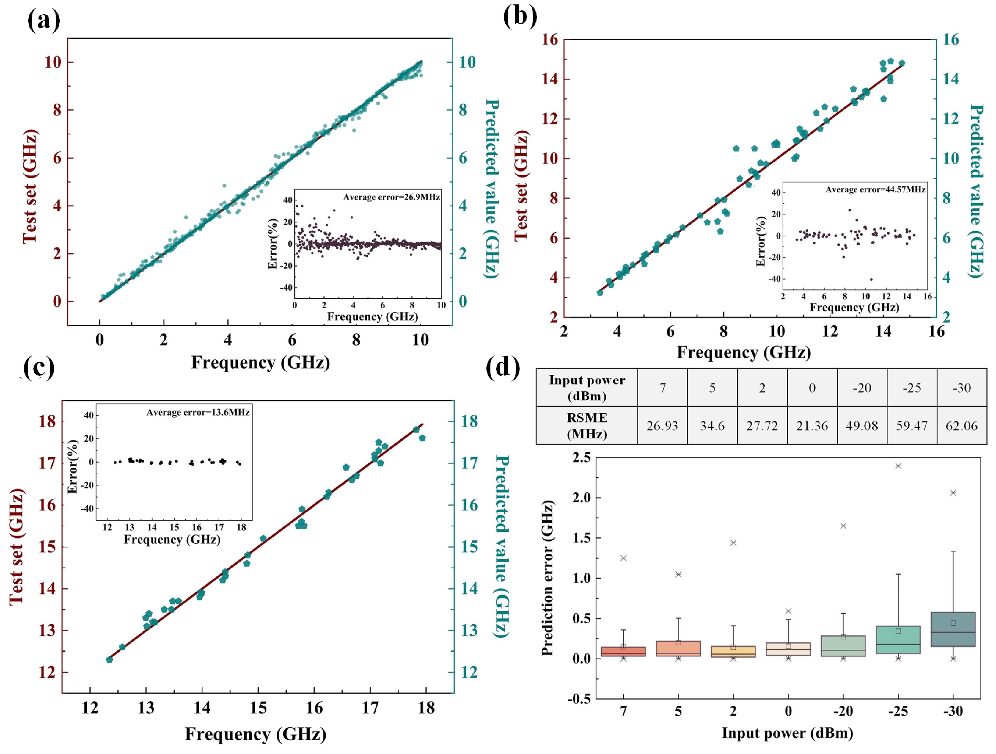
| LNOI PM (this work) | 0–10 GHz | 26.9 MHz | −30 dBm | √ |
| 3–15 GHz | 44.57 MHz | |||
| 12–18 GHz | 13.6 MHz |
Disclaimer/Publisher’s Note: The statements, opinions and data contained in all publications are solely those of the individual author(s) and contributor(s) and not of MDPI and/or the editor(s). MDPI and/or the editor(s) disclaim responsibility for any injury to people or property resulting from any ideas, methods, instructions or products referred to in the content. |
© 2024 by the authors. Licensee MDPI, Basel, Switzerland. This article is an open access article distributed under the terms and conditions of the Creative Commons Attribution (CC BY) license (https://creativecommons.org/licenses/by/4.0/).
Share and Cite
Jia, Q.; Xiang, Z.; Li, D.; Liu, J.; Li, J. Machine-Learning-Assisted Instantaneous Frequency Measurement Method Based on Thin-Film Lithium Niobate on an Insulator Phase Modulator for Radar Detection. Sensors 2024, 24, 1489. https://doi.org/10.3390/s24051489
Jia Q, Xiang Z, Li D, Liu J, Li J. Machine-Learning-Assisted Instantaneous Frequency Measurement Method Based on Thin-Film Lithium Niobate on an Insulator Phase Modulator for Radar Detection. Sensors. 2024; 24(5):1489. https://doi.org/10.3390/s24051489
Chicago/Turabian StyleJia, Qianqian, Zichuan Xiang, Dechen Li, Jianguo Liu, and Jinye Li. 2024. "Machine-Learning-Assisted Instantaneous Frequency Measurement Method Based on Thin-Film Lithium Niobate on an Insulator Phase Modulator for Radar Detection" Sensors 24, no. 5: 1489. https://doi.org/10.3390/s24051489