
Development of the Tele-Measurement of Plasma Uniformity via Surface Wave Information (TUSI) Probe for Non-Invasive In-Situ Monitoring of Electron Density Uniformity in Plasma Display Fabrication Process

 , , , ,
Abstract
:1. Introduction
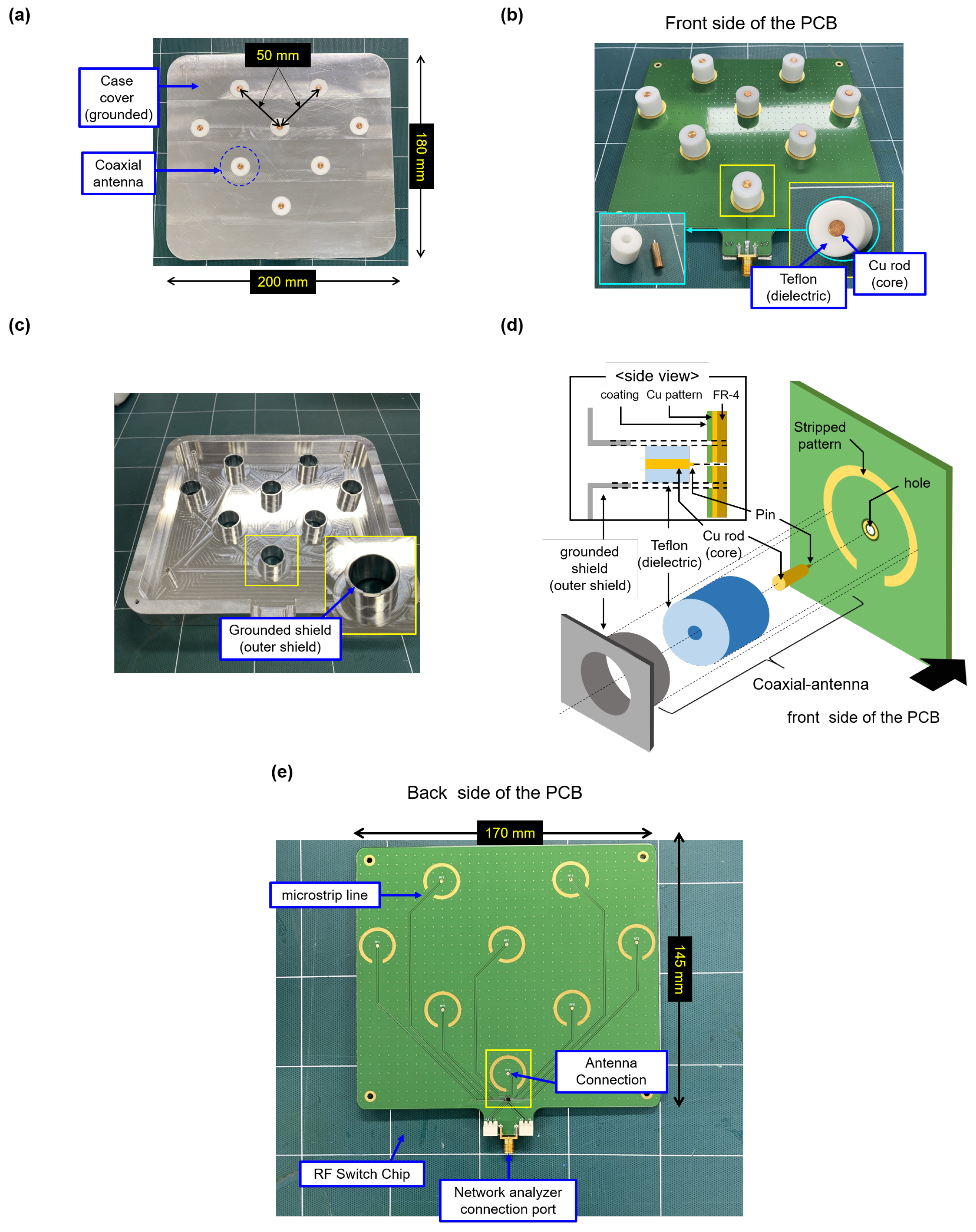
2. Configuration
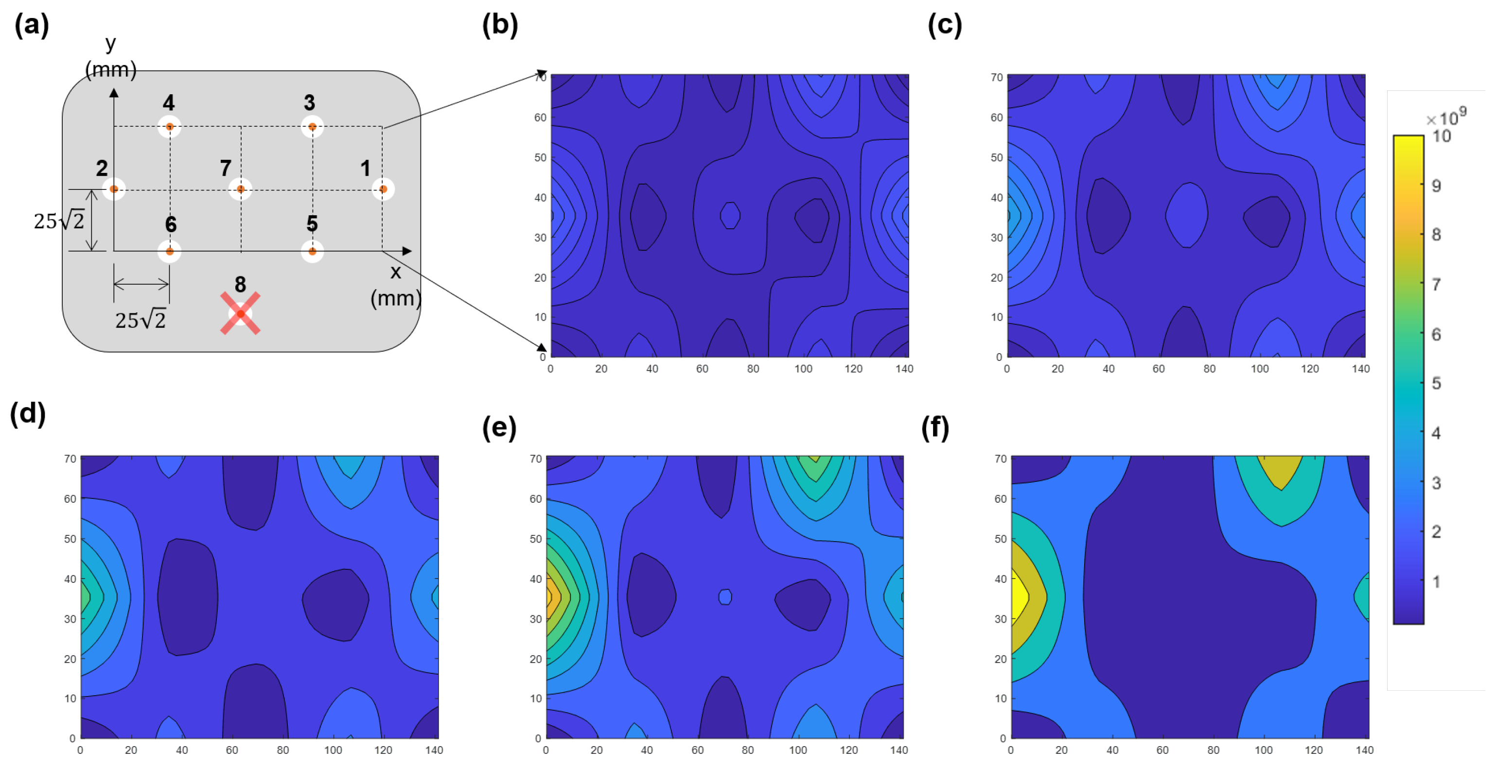
3. Validation of the TUSI Probe with the Cutoff Probe
3.1. Experiment Setup
3.2. Results and Discussion
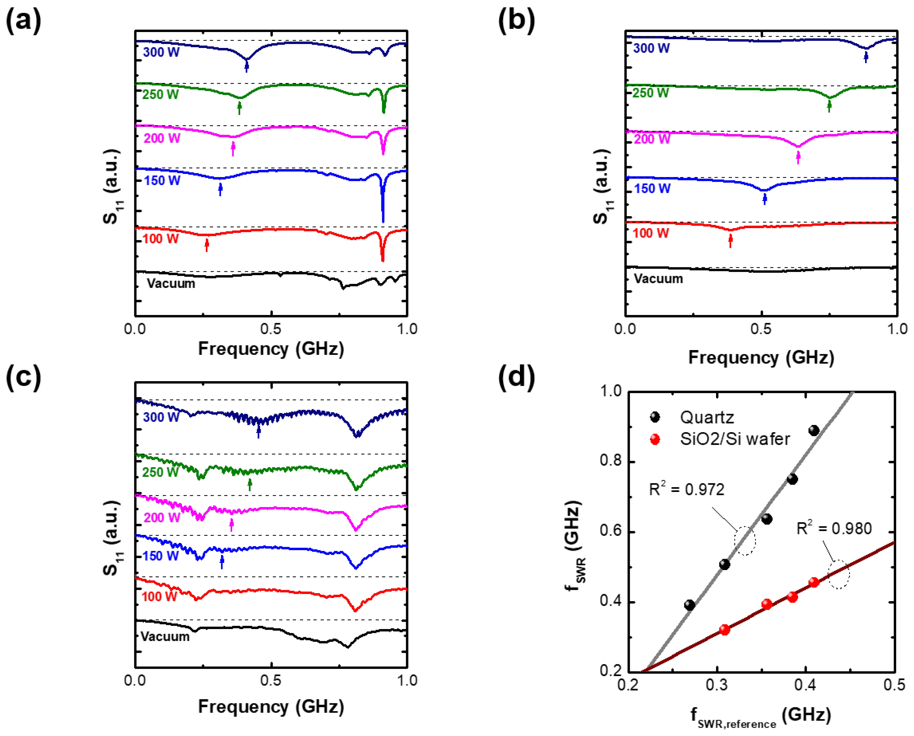
4. Demonstration of the TUSI Probe Working Beneath a Quartz and a SiO(100 nm)/Si Wafer
4.1. Experiment Setup
4.2. Results and Discussion
5. Conclusions
Author Contributions
Funding
Institutional Review Board Statement
Informed Consent Statement
Data Availability Statement
Conflicts of Interest
References
- Bogaerts, A.; Tu, X.; Whitehead, J.C.; Centi, G.; Lefferts, L.; Guaitella, O.; Azzolina-Jury, F.; Kim, H.H.; Murphy, A.B.; Schneider, W.F.; et al. The 2020 plasma catalysis roadmap. J. Phys. D Appl. Phys. 2020, 53, 443001. [Google Scholar] [CrossRef]
- Laroussi, M.; Bekeschus, S.; Keidar, M.; Bogaerts, A.; Fridman, A.; Lu, X.; Ostrikov, K.; Hori, M.; Stapelmann, K.; Miller, V.; et al. Low-temperature plasma for biology, hygiene, and medicine: Perspective and roadmap. IEEE Trans. Radiat. Plasma Med. Sci. 2022, 6, 127–157. [Google Scholar] [CrossRef]
- Lieberman, M.A.; Lichtenberg, A.J. Principles of Plasma Discharges and Materials Processing; John Wiley & Sons: Hoboken, NJ, USA, 2005; pp. 1–22, xxxv. [Google Scholar]
- You, Y.B.; Lee, Y.S.; Kim, S.J.; Cho, C.H.; Seong, I.H.; Jeong, W.N.; Choi, M.S.; You, S.J. Influence of Additive N2 on O2 Plasma Ashing Process in Inductively Coupled Plasma. Nanomaterials 2022, 12, 3798. [Google Scholar] [CrossRef] [PubMed]
- Lee, Y.; Yeom, H.; Choi, D.; Kim, S.; Lee, J.; Kim, J.; Lee, H.; You, S. Database Development of SiO2 Etching with Fluorocarbon Plasmas Diluted with Various Noble Gases of Ar, Kr, and Xe. Nanomaterials 2022, 12, 3828. [Google Scholar] [CrossRef] [PubMed]
- Seong, I.H.; Lee, J.J.; Cho, C.H.; Lee, Y.S.; Kim, S.J.; You, S.J. Characterization of SiO2 Over Poly-Si Mask Etching in Ar/C4F8 Capacitively Coupled Plasma. Appl. Sci. Converg. Technol. 2021, 30, 176–182. [Google Scholar] [CrossRef]
- Kim, S.; Lee, Y.; Cho, C.; Choi, M.; Seong, I.; Lee, J.; Kim, D.; You, S. Observation of prior light emission before arcing development in a low-temperature plasma with multiple snapshot analysis. Sci. Rep. 2022, 12, 20976. [Google Scholar] [CrossRef]
- Yang, R.; Chen, R. Real-time plasma process condition sensing and abnormal process detection. Sensors 2010, 10, 5703–5723. [Google Scholar] [CrossRef] [Green Version]
- Abbas, M.A.; Dijk, L.V.; Jahromi, K.E.; Nematollahi, M.; Harren, F.J.; Khodabakhsh, A. Broadband time-resolved absorption and dispersion spectroscopy of methane and ethane in a plasma using a mid-infrared dual-comb spectrometer. Sensors 2020, 20, 6831. [Google Scholar] [CrossRef]
- Wang, J.; Ji, W.; Du, Q.; Xing, Z.; Xie, X.; Zhang, Q. A Long Short-Term Memory Network for Plasma Diagnosis from Langmuir Probe Data. Sensors 2022, 22, 4281. [Google Scholar] [CrossRef]
- Kim, S.; Lee, J.; Lee, Y.; Cho, C.; You, S. Crossing Frequency Method Applicable to Intermediate Pressure Plasma Diagnostics Using the Cutoff Probe. Sensors 2022, 22, 1291. [Google Scholar] [CrossRef]
- Kim, S.; Lee, S.; You, Y.; Lee, Y.; Seong, I.; Cho, C.; Lee, J.; You, S. Development of the Measurement of Lateral Electron Density (MOLE) Probe Applicable to Low-Pressure Plasma Diagnostics. Sensors 2022, 22, 5487. [Google Scholar] [CrossRef] [PubMed]
- Kim, S.J.; Lee, J.J.; Lee, Y.S.; Yeom, H.J.; Lee, H.C.; Kim, J.H.; You, S.J. Computational Characterization of Microwave Planar Cutoff Probes for Non-Invasive Electron Density Measurement in Low-Temperature Plasma: Ring-and Bar-Type Cutoff Probes. Appl. Sci. 2020, 10, 7066. [Google Scholar] [CrossRef]
- Kim, K.K.; Lee, J.J.; Kim, S.J.; Cho, C.H.; Yoo, S.W.; You, S.J. Development of High-precision RF Sensor. Appl. Sci. Converg. Technol. 2019, 28, 88–92. [Google Scholar] [CrossRef]
- Kwon, J.W.; Ryu, S.; Park, J.; Lee, H.; Jang, Y.; Park, S.; Kim, G.H. Development of virtual metrology using plasma information variables to predict Si etch profile processed by SF6/O2/Ar capacitively coupled plasma. Materials 2021, 14, 3005. [Google Scholar] [CrossRef]
- Yeom, H.; Kim, J.; Choi, D.; Choi, E.; Yoon, M.; Seong, D.; You, S.J.; Lee, H.C. Flat cutoff probe for real-time electron density measurement in industrial plasma processing. Plasma Sources Sci. Technol. 2020, 29, 035016. [Google Scholar] [CrossRef]
- Kim, S.; Lee, J.; Lee, Y.; Kim, D.; You, S. Finding the optimum design of the planar cutoff probe through a computational study. AIP Adv. 2021, 11, 025241. [Google Scholar] [CrossRef]
- Seong, I.; Kim, S.; Lee, Y.; Cho, C.; Lee, J.; Jeong, W.; You, Y.; You, S. Development of a Noninvasive Real-Time Ion Energy Distribution Monitoring System Applicable to Collisional Plasma Sheath. Sensors 2022, 22, 6254. [Google Scholar] [CrossRef]
- Kim, S.; Seong, I.; Lee, Y.; Cho, C.; Jeong, W.; You, Y.; Lee, J.; You, S. Development of a High-Linearity Voltage and Current Probe with a Floating Toroidal Coil: Principle, Demonstration, Design Optimization, and Evaluation. Sensors 2022, 22, 5871. [Google Scholar] [CrossRef]
- Kim, D.; You, S.; Kim, S.; Kim, J.; Lee, J.; Kang, W.; Hur, M. Planar cutoff probe for measuring the electron density of low-pressure plasmas. Plasma Sources Sci. Technol. 2019, 28, 015004. [Google Scholar] [CrossRef]
- Ishikawa, K.; Karahashi, K.; Ishijima, T.; Cho, S.I.; Elliott, S.; Hausmann, D.; Mocuta, D.; Wilson, A.; Kinoshita, K. Progress in nanoscale dry processes for fabrication of high-aspect-ratio features: How can we control critical dimension uniformity at the bottom? Jpn. J. Appl. Phys. 2018, 57, 06JA01. [Google Scholar] [CrossRef]
- Mahoney, L.; Carter, D.; Roberts, S.; Roche, G. Wafer Probe for Measuring Plasma and Surface Characteristics in Plasma Processing Environments. U.S. Patent US20050011611A1, 14 December 2004. [Google Scholar]
- Kim, Y.C.; Jang, S.H.; Oh, S.J.; Lee, H.C.; Chung, C.W. Two-dimensional-spatial distribution measurement of electron temperature and plasma density in low temperature plasmas. Rev. Sci. Instruments 2013, 84, 053505. [Google Scholar] [CrossRef] [PubMed]
- Kim, I.J.; Yun, I. Real-time plasma uniformity measurement technique using optical emission spectroscopy with revolving module. IEEE Sensors J. 2018, 19, 2356–2361. [Google Scholar] [CrossRef]
- Ogawa, D.; Nakamura, K.; Sugai, H. Experimental validity of double-curling probe method in film-depositing plasma. Plasma Sources Sci. Technol. 2021, 30, 085009. [Google Scholar] [CrossRef]
- Liang, I.; Nakamura, K.; Sugai, H. Modeling microwave resonance of curling probe for density measurements in reactive plasmas. Appl. Phys. Express 2011, 4, 066101. [Google Scholar] [CrossRef]
- Schulz, C.; Styrnoll, T.; Awakowicz, P.; Rolfes, I. The planar multipole resonance probe: Challenges and prospects of a planar plasma sensor. IEEE Trans. Instrum. Meas. 2014, 64, 857–864. [Google Scholar] [CrossRef]
- Dine, S.; Booth, J.P.; Curley, G.A.; Corr, C.; Jolly, J.; Guillon, J. A novel technique for plasma density measurement using surface-wave transmission spectra. Plasma Sources Sci. Technol. 2005, 14, 777. [Google Scholar] [CrossRef]
- Margraf, M. QucsStudio—A Free and Powerful Circuit Simulator. Available online: http://qucsstudio.de (accessed on 1 January 2022).
- Lee, S.W. Design of an Inductively Coupled Plasma Source with Consideration of Electrical Properties and its Practical Issues. Appl. Sci. Converg. Technol. 2009, 18, 176–185. [Google Scholar] [CrossRef] [Green Version]
- Kim, D.W.; You, S.; Kim, J.; Chang, H.; Oh, W.Y. Computational comparative study of microwave probes for plasma density measurement. Plasma Sources Sci. Technol. 2016, 25, 035026. [Google Scholar] [CrossRef]
- Kim, D.W.; You, S.; Kwon, J.; You, K.; Seo, B.; Kim, J.; Yoon, J.S.; Oh, W.Y. Reproducibility of the cutoff probe for the measurement of electron density. Phys. Plasmas 2016, 23, 063501. [Google Scholar] [CrossRef]
- Seo, B.; Kim, D.W.; Kim, J.H.; You, S. Investigation of reliability of the cutoff probe by a comparison with Thomson scattering in high density processing plasmas. Phys. Plasmas 2017, 24, 123502. [Google Scholar] [CrossRef] [Green Version]
- Kim, S.; Lee, J.; Kim, D.; Kim, J.; You, S. A transmission line model of the cutoff probe. Plasma Sources Sci. Technol. 2019, 28, 055014. [Google Scholar] [CrossRef]
- Kim, S.; Lee, J.; Lee, Y.; Kim, D.; You, S. Effect of an inhomogeneous electron density profile on the transmission microwave frequency spectrum of the cutoff probe. Plasma Sources Sci. Technol. 2020, 29, 125014. [Google Scholar] [CrossRef]


| V (V) | V (V) | V (V) | RF1 | RF2 | RF3 | RF4 | RF5 | RF6 | RF7 | RF8 |
|---|---|---|---|---|---|---|---|---|---|---|
| 0 | 0 | 0 | ⋆ | - | - | - | - | - | - | - |
| 0 | 0 | 1.8 | - | ⋆ | - | - | - | - | - | - |
| 0 | 1.8 | 0 | - | - | ⋆ | - | - | - | - | - |
| 0 | 1.8 | 1.8 | - | - | - | ⋆ | - | - | - | - |
| 1.8 | 0 | 0 | - | - | - | - | ⋆ | - | - | - |
| 1.8 | 0 | 1.8 | - | - | - | - | - | ⋆ | - | - |
| 1.8 | 1.8 | 0 | - | - | - | - | - | - | ⋆ | - |
| 1.8 | 1.8 | 1.8 | - | - | - | - | - | - | - | ⋆ |
Disclaimer/Publisher’s Note: The statements, opinions and data contained in all publications are solely those of the individual author(s) and contributor(s) and not of MDPI and/or the editor(s). MDPI and/or the editor(s) disclaim responsibility for any injury to people or property resulting from any ideas, methods, instructions or products referred to in the content. |
© 2023 by the authors. Licensee MDPI, Basel, Switzerland. This article is an open access article distributed under the terms and conditions of the Creative Commons Attribution (CC BY) license (https://creativecommons.org/licenses/by/4.0/).
Share and Cite
Kim, S.-J.; Choi, M.-S.; Lee, S.-H.; Jeong, W.-N.; Lee, Y.-S.; Seong, I.-H.; Cho, C.-H.; Kim, D.-W.; You, S.-J. Development of the Tele-Measurement of Plasma Uniformity via Surface Wave Information (TUSI) Probe for Non-Invasive In-Situ Monitoring of Electron Density Uniformity in Plasma Display Fabrication Process. Sensors 2023, 23, 2521. https://doi.org/10.3390/s23052521
Kim S-J, Choi M-S, Lee S-H, Jeong W-N, Lee Y-S, Seong I-H, Cho C-H, Kim D-W, You S-J. Development of the Tele-Measurement of Plasma Uniformity via Surface Wave Information (TUSI) Probe for Non-Invasive In-Situ Monitoring of Electron Density Uniformity in Plasma Display Fabrication Process. Sensors. 2023; 23(5):2521. https://doi.org/10.3390/s23052521
Chicago/Turabian StyleKim, Si-Jun, Min-Su Choi, Sang-Ho Lee, Won-Nyoung Jeong, Young-Seok Lee, In-Ho Seong, Chul-Hee Cho, Dae-Woong Kim, and Shin-Jae You. 2023. "Development of the Tele-Measurement of Plasma Uniformity via Surface Wave Information (TUSI) Probe for Non-Invasive In-Situ Monitoring of Electron Density Uniformity in Plasma Display Fabrication Process" Sensors 23, no. 5: 2521. https://doi.org/10.3390/s23052521