


Novel Deposition Method of Crosslinked Polyethylene Thin Film for Low-Refractive-Index Mid-Infrared Optical Coatings

Abstract
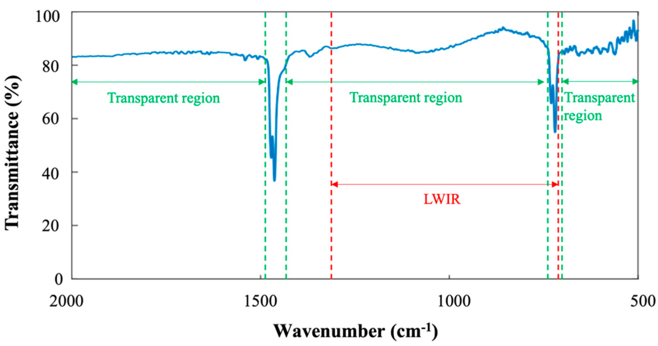
:1. Introduction
2. Deposition Method of XPE Thin Film
3. Monte Carlo Simulation
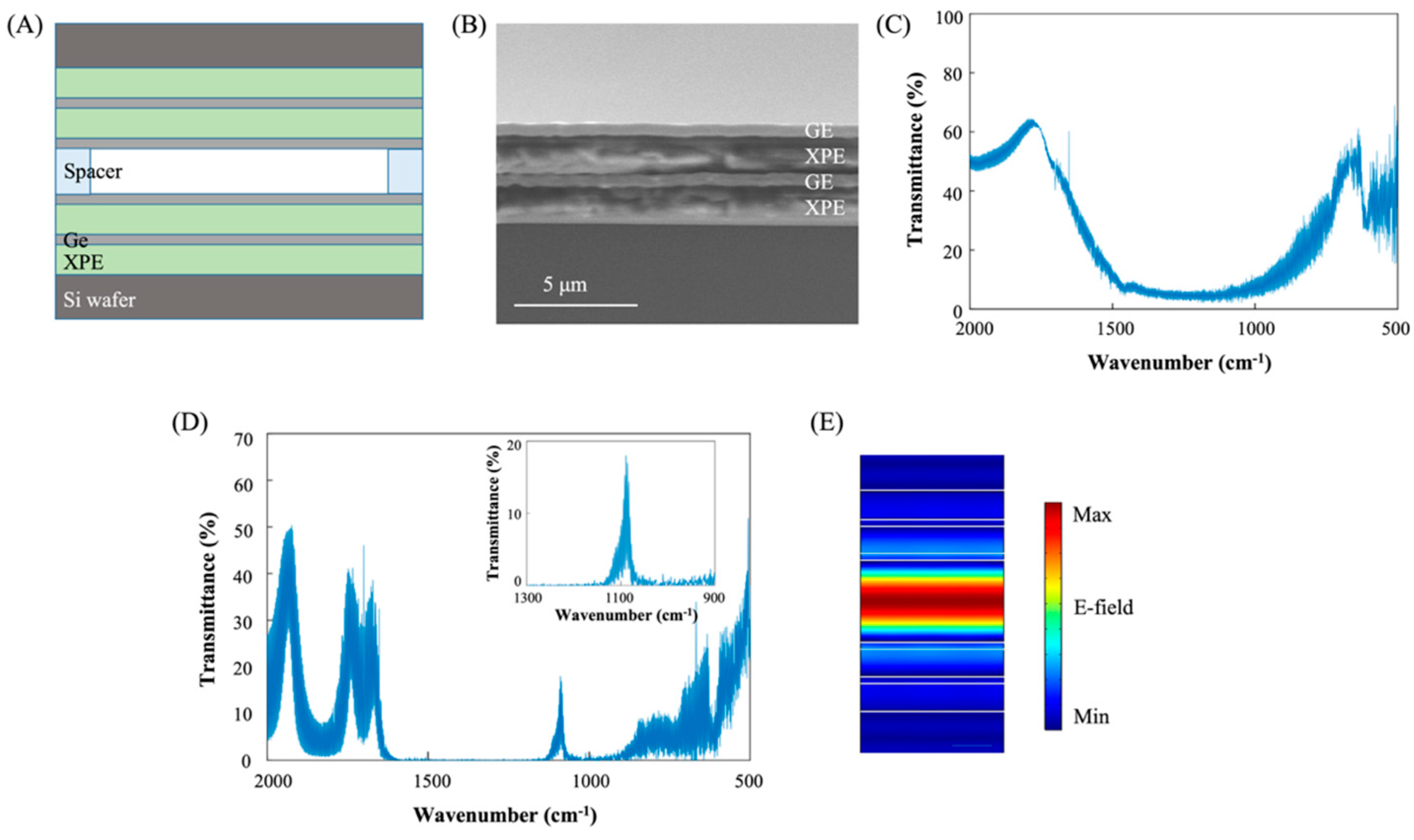
4. Mid-IR Optical Filter Fabrication
5. Discussion
6. Conclusions
Supplementary Materials
Author Contributions
Funding
Institutional Review Board Statement
Informed Consent Statement
Data Availability Statement
Conflicts of Interest
References
- Pavia, D.L.; Lampman, G.M.; Kriz, G.S.; Vyvyan, J.R. Introduction to Spectroscopy; Cengage Learning: Stamford, CT, USA, 2015. [Google Scholar]
- Griffiths, P.R.; De Haseth, J.A. Fourier Transform Infrared Spectroscopy; Wiley: New York, NY, USA, 2007. [Google Scholar]
- Gmachl, C.; Capasso, F.; Sivco, D.L.; Cho, A.Y. Recent progress in quantum cascade lasers and applications. Rep. Prog. Phys. 2001, 64, 1533–1601. [Google Scholar] [CrossRef]
- Jeon, T.; Nateghi, A.; Jones, W.M.; Choi, C.; Cardenas, J.P.; Ross, C.; Scherer, A. Development of a Compact and Robust Mid-Infrared Spectrometer by Using a Silicon/Air Hyperspectral Filter. ACS Photonics 2022, 9, 68–73. [Google Scholar] [CrossRef]
- Muraviev, A.V.; Vodopyanov, K.L. Massively parallel sensing of trace molecules and their isotopologues with broadband subharmonic mid-infrared frequency combs. Nat. Photonics 2018, 12, 209–214. [Google Scholar] [CrossRef]
- Scalari, G.; Faist, J.; Picque, N. On-chip mid-infrared and THz frequency combs for spectroscopy. Appl. Phys. Lett. 2019, 114, 150401. [Google Scholar] [CrossRef]
- Tittl, A.; Leitis, A.; Liu, M.; Yesilkoy, F.; Choi, D.Y.; Neshev, D.N.; Kivshar, Y.S.; Altug, H. Imaging-based molecular barcoding with pixelated dielectric metasurfaces. Science 2018, 360, 1105–1109. [Google Scholar] [CrossRef] [PubMed]
- Leitis, A.; Tittl, A.; Liu, M.; Lee, B.H.; Gu, M.B.; Kivshar, Y.S.; Altug, H. Angle-multiplexed all-dielectric metasurfaces for broadband molecular fingerprint retrieval. Sci. Adv. 2019, 5, eaaw2871. [Google Scholar] [CrossRef] [PubMed]
- Soref, R. Mid-infrared photonics in silicon and germanium. Nat. Photonics 2010, 4, 495–497. [Google Scholar] [CrossRef]
- Burnett, J.H.; Kaplan, S.G.; Stover, E.; Phenis, A. Refractive index measurement of Ge. Proc. SPIE 2016, 9974, 99740X. [Google Scholar]
- Chandler-Horowitz, D.; Amirtharaj, P.M. High-accuracy; midinfrared (450 cm−1 ⩽ ω ⩽ 4000 cm−1) refractive index values of silicon. J. Appl. Phys. 2005, 97, 123526. [Google Scholar] [CrossRef]
- Blodgett, D.W.; Yang, D.; Walts, S.C.; Thomas, M.E. Measurement of the temperature-dependent refractive index and relative photoelastic constant of zinc sulfide. Proc. SPIE 2001, 4375, 224–234. [Google Scholar]
- Qi, H.; Zhang, X.; Jiang, M.; Wang, Q.; Li, D. Optical Constants of Zinc Selenide in Visible and Infrared Spectral Ranges. J. Appl. Spectrosc. 2017, 84, 679–682. [Google Scholar] [CrossRef]
- Emadi, A.; Wu, H.; de Graaf, G.; Wolffenbuttel, R. Design and implementation of a sub-nm resolution microspectrometer based on a Linear-Variable Optical Filter. Opt. Express 2012, 20, 489. [Google Scholar] [CrossRef] [PubMed]
- Musfir, P.N.; Nampoori, V.P.N.; Thomas, S. Variations in the linear and nonlinear refractive indices of chalcogenide glass thin films for photonic applications. Mater. Res. Express 2019, 6, 115207. [Google Scholar] [CrossRef]
- Lin, R.; Chen, F.; Zhang, X.; Huang, Y.; Song, B.; Dai, S.; Zhang, X.; Ji, W. Mid-infrared optical properties of chalcogenide glasses within tin-antimony-selenium ternary system. Opt. Express 2017, 25, 25674–25688. [Google Scholar] [CrossRef]
- Businaro, L.; Limaj, O.; Giliberti, V.; Ortolani, M.; Di Gaspare, A.; Grenci, G.; Lupi, S. Mid-infrared nanoantenna arrays on silicon and CaF2 substrates for sensing applications. Microelectron. Eng. 2012, 97, 197–200. [Google Scholar] [CrossRef]
- Su, W.; Li, B.; Liu, D.; Zhang, F. The determination of infrared optical constants of rare earth fluorides by classical Lorentz oscillator model. J. Phys. Appl. Phys. 2007, 40, 3343–3347. [Google Scholar] [CrossRef]
- Wang, Y.; Abe, Y.; Matsuura, Y.; Miyagi, M.; Uyama, H. Refractive indices and extinction coefficients of polymers for the mid-infrared region. Appl. Opt. 1998, 37, 7091–7095. [Google Scholar] [CrossRef]
- Mellbring, O.; Øiseth, S.K.; Krozer, A.; Lausmaa, J.; Hjertberg, T. Spin Coating and Characterization of Thin High-Density Polyethylene Films. Macromolecules 2001, 34, 7496–7503. [Google Scholar] [CrossRef]
- Iuff, P.P.; White, M. Thermal degradation of polyethylene and polytetrafluoroethylene during vacuum evaporation. Vacuum 1968, 18, 437–440. [Google Scholar]
- Qu, B.; Ranby, B. Radiation crosslinking of polyethylene with electron beam at different temperature. Polym. Eng. Sci. 1995, 35, 1161–1166. [Google Scholar] [CrossRef]
- Tretinnikov, O.N.; Ogata, S.; Ikada, Y. Surface crosslinking of polyethylene by electron beam irradiation in air. Polymer 1998, 39, 6115–6120. [Google Scholar] [CrossRef]
- Gulmine, J.; Janissek, P.; Heise, H.; Akcelrud, L. Polyethylene characterization by FTIR. Polym. Test. 2002, 21, 557–563. [Google Scholar] [CrossRef]
- De Geyter, N.; Morent, R.; Leys, C. Surface characterization of plasma-modified polyethylene by contact angle experiments and ATR-FTIR spectroscopy. Surf. Interface Anal. 2008, 40, 608–611. [Google Scholar] [CrossRef]
- Martyniuk, M.; Silva, K.K.M.B.D.; Putrino, G.; Kala, H.; Tripathi, D.K.; Gill, G.S.; Faraone, L. Optical Microelectromechanical Systems Technologies for Spectrally Adaptive Sensing and Imaging. Adv. Funct. Mater. 2022, 32, 2103153. [Google Scholar] [CrossRef]
- Nottingham, W.B. Thermionic emission from tungsten and thoriated tungsten filaments. Phys. Rev. 1936, 49, 78–97. [Google Scholar] [CrossRef]
- Drouin, D.; Couture, A.R.; Joly, D.; Tastet, X.; Aimez, V.; Gauvin, R. CASINO V2.42—A Fast and Easy-to-use Modeling Tool for Scanning Electron Microscopy and Microanalysis Users. Scanning 2007, 29, 92–101. [Google Scholar] [CrossRef] [PubMed]
- Khlyustova, A.; Cheng, Y.; Yang, R. Vapor-deposited functional polymer thin films in biological applications. J. Mater. Chem. B 2020, 8, 6588–6609. [Google Scholar] [CrossRef]
- Yang, C.; Zhang, D.; Wang, D.; Luan, H.; Chen, X.; Yang, W. In Situ Polymerized MXene/Polypyrrole/Hydroxyethyl Cellulose-Based Flexible Strain Sensor Enabled by Machine Learning for Handwriting Recognition. ACS Appl. Mater. Interfaces 2023, 15, 5811–5821. [Google Scholar] [CrossRef]
- Elanjeitsenni, V.P.; Vadivu, K.S. A review on thin films, conducting polymers as sensor devices. Mater. Res. Express 2022, 9, 022001. [Google Scholar] [CrossRef]


| Materials | Refractive Index at 10 µm | Transparent on between 5 µm to 20 µm |
|---|---|---|
| Polyethylene | 1.53 | Transparent up to 20 µm, except for two peaks positioned near 6.8 µm and 13.8 µm |
| Chalcogenide Glass | Over 2.5 (change depending on the composition) | Transparent up to 20 µm |
| ZnS | 2.2 | Transparent up to 14 µm |
| ZnSe | 2.4 | Transparent up to 14 µm and transmittance gradually decrease up to 20 µm |
| CaF2 | 1.3 | Transparent up to 8 µm and transmittance gradually decrease and become zero at about 12 µm |
Disclaimer/Publisher’s Note: The statements, opinions and data contained in all publications are solely those of the individual author(s) and contributor(s) and not of MDPI and/or the editor(s). MDPI and/or the editor(s) disclaim responsibility for any injury to people or property resulting from any ideas, methods, instructions or products referred to in the content. |
© 2023 by the authors. Licensee MDPI, Basel, Switzerland. This article is an open access article distributed under the terms and conditions of the Creative Commons Attribution (CC BY) license (https://creativecommons.org/licenses/by/4.0/).
Share and Cite
Jeon, T.; Myung, J.; Choi, C.; Shayegan, K.; Lewis, S.M.; Scherer, A. Novel Deposition Method of Crosslinked Polyethylene Thin Film for Low-Refractive-Index Mid-Infrared Optical Coatings. Sensors 2023, 23, 9810. https://doi.org/10.3390/s23249810
Jeon T, Myung J, Choi C, Shayegan K, Lewis SM, Scherer A. Novel Deposition Method of Crosslinked Polyethylene Thin Film for Low-Refractive-Index Mid-Infrared Optical Coatings. Sensors. 2023; 23(24):9810. https://doi.org/10.3390/s23249810
Chicago/Turabian StyleJeon, Taeyoon, Jieun Myung, Changsoon Choi, Komron Shayegan, Scott M. Lewis, and Axel Scherer. 2023. "Novel Deposition Method of Crosslinked Polyethylene Thin Film for Low-Refractive-Index Mid-Infrared Optical Coatings" Sensors 23, no. 24: 9810. https://doi.org/10.3390/s23249810