
Photonic Integrated Circuit Based Temperature Sensor for Out-of-Autoclave Composite Parts Production Monitoring
 , , ,
, , ,
Abstract
:1. Introduction
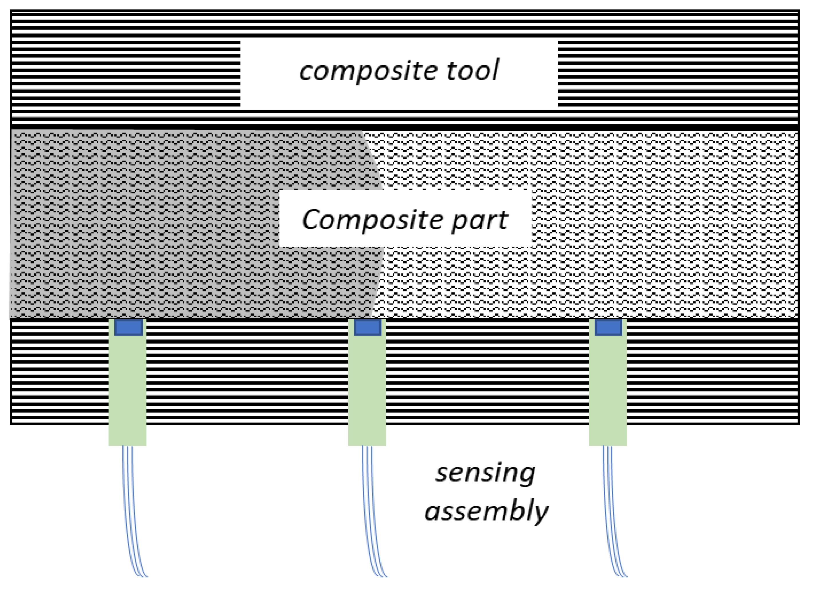
2. Concept
3. Materials and Methods
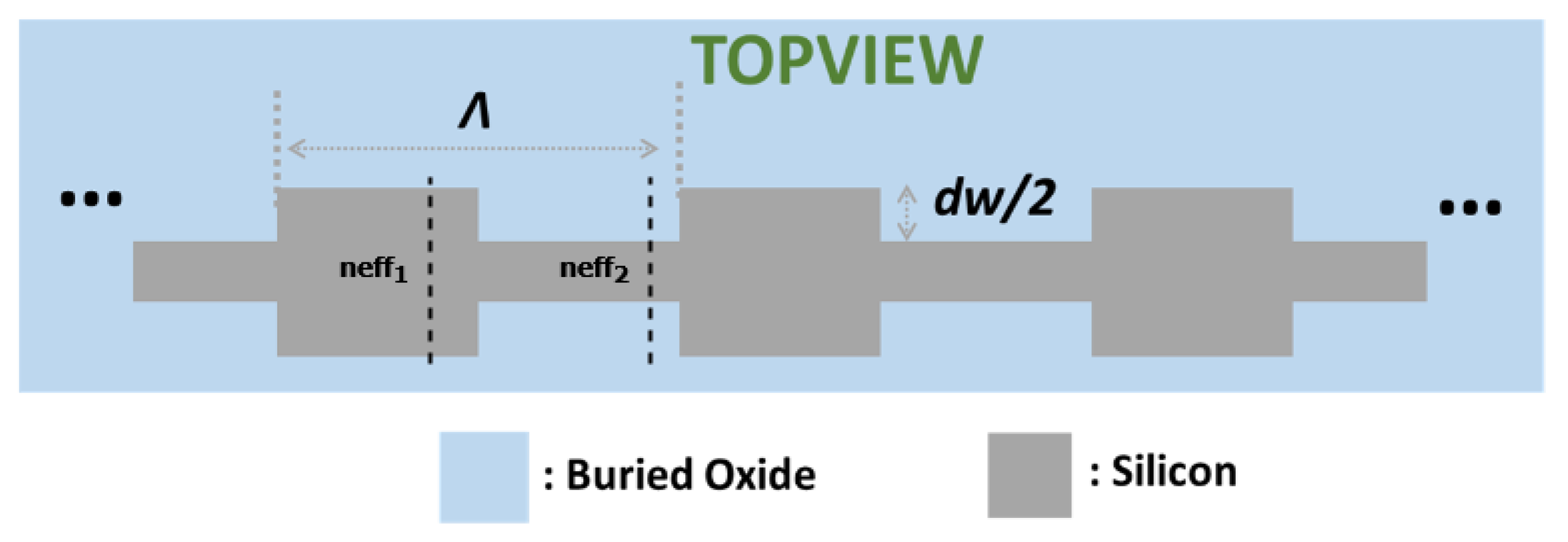
3.1. Design of the Bragg Grating
3.1.1. Waveguide Modes Calculation
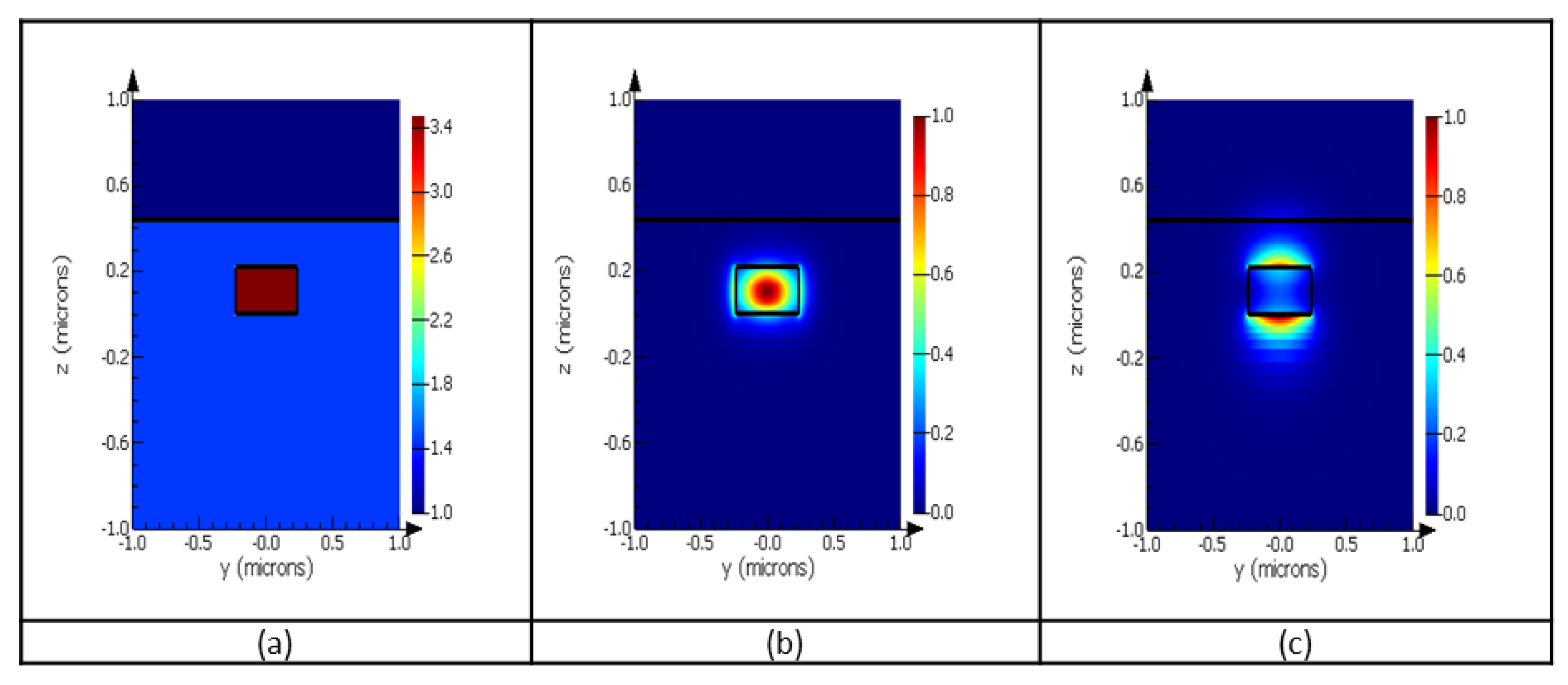
3.1.2. Propagation Simulation
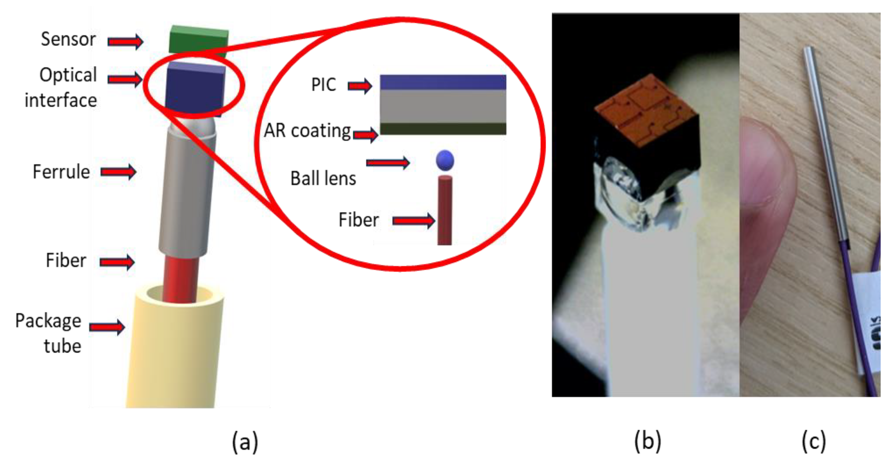
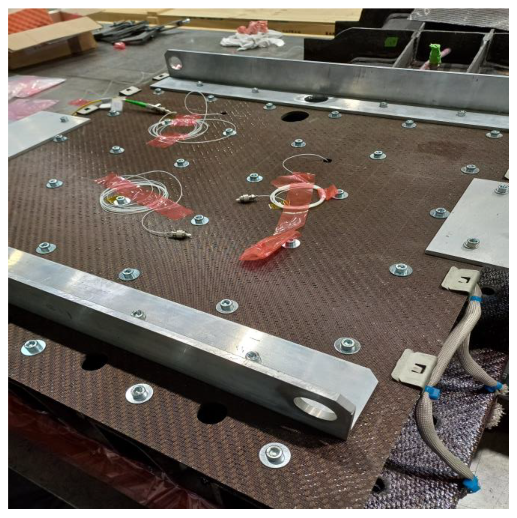
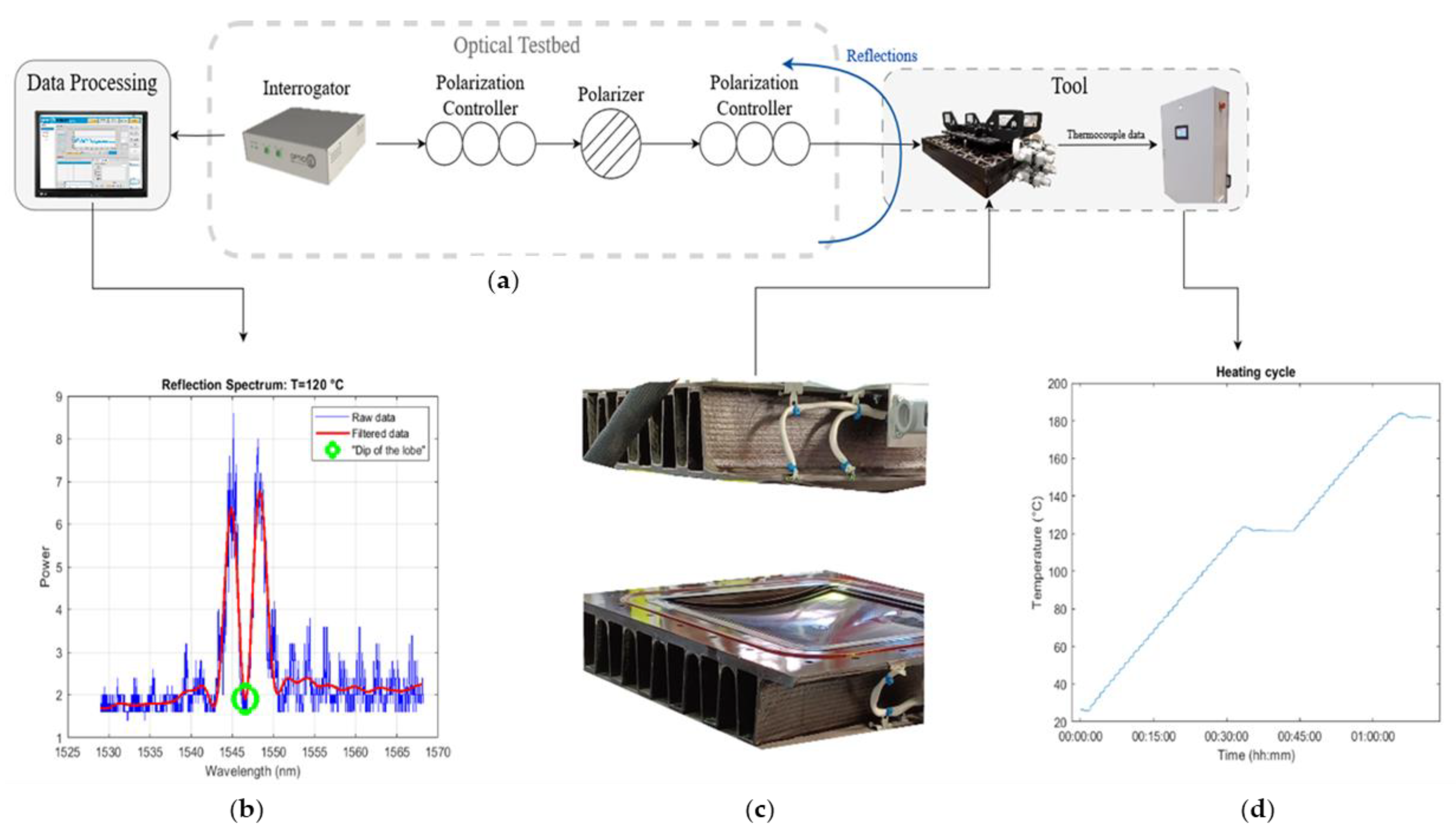
3.2. Experimental Characterization
4. Results and Discussion
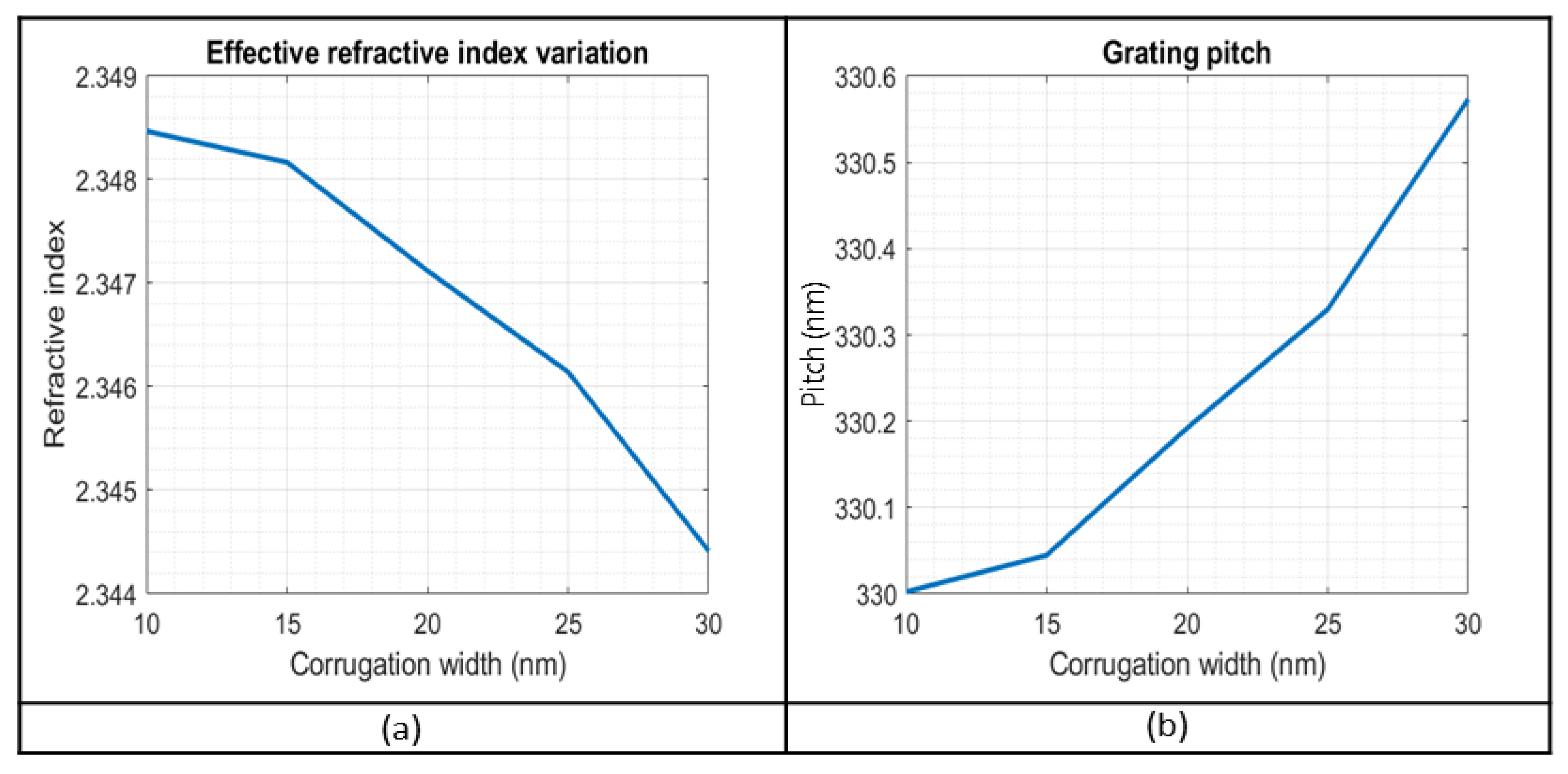
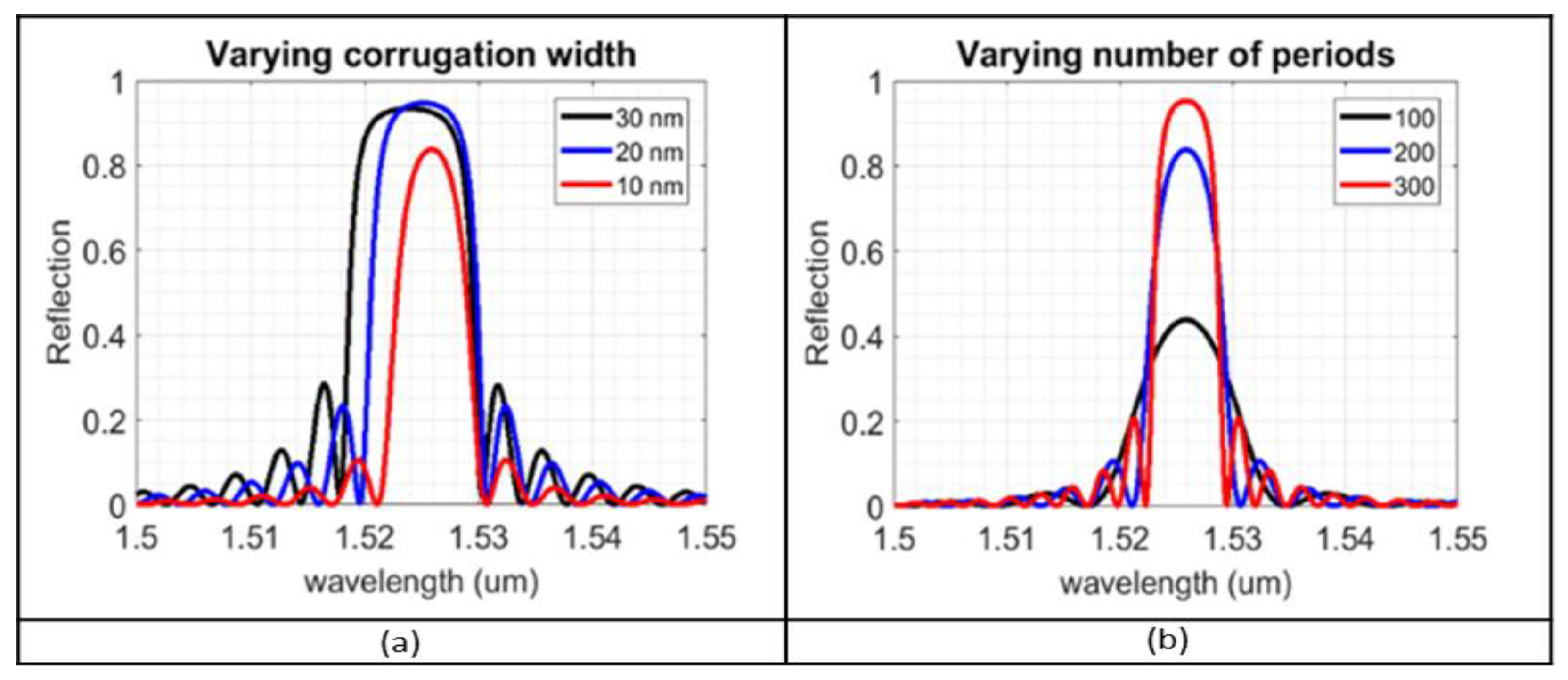
4.1. Design of the Bragg Grating
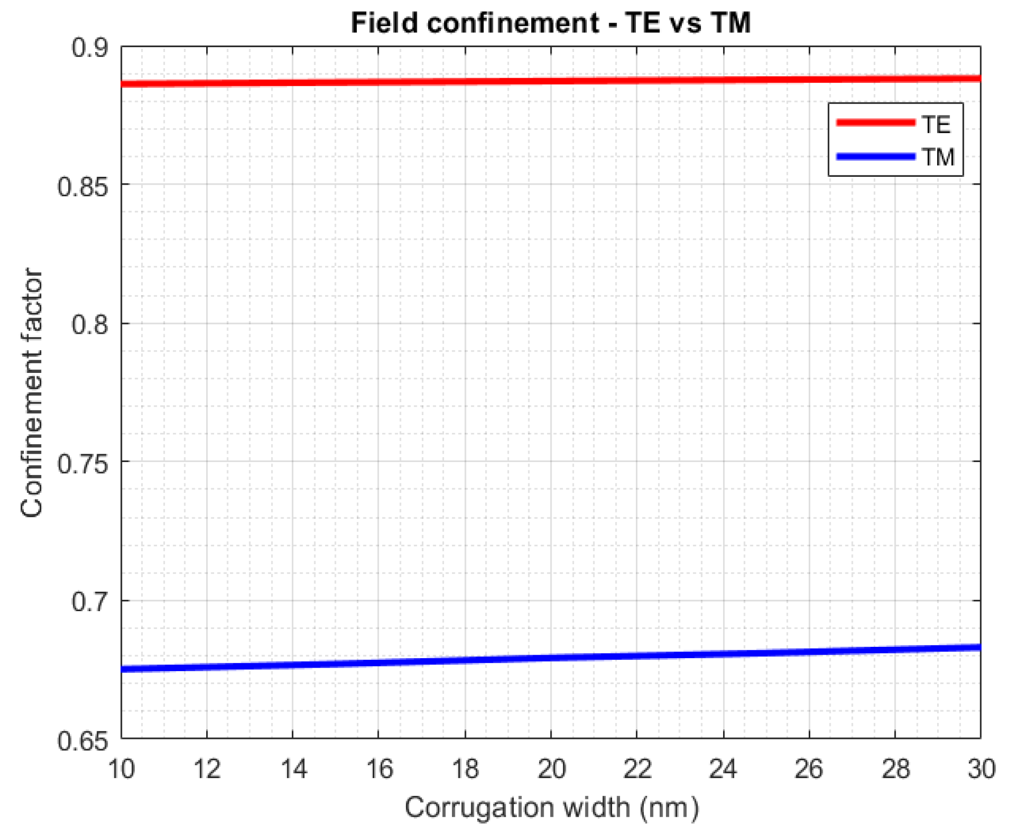
4.1.1. Waveguide Mode Calculation
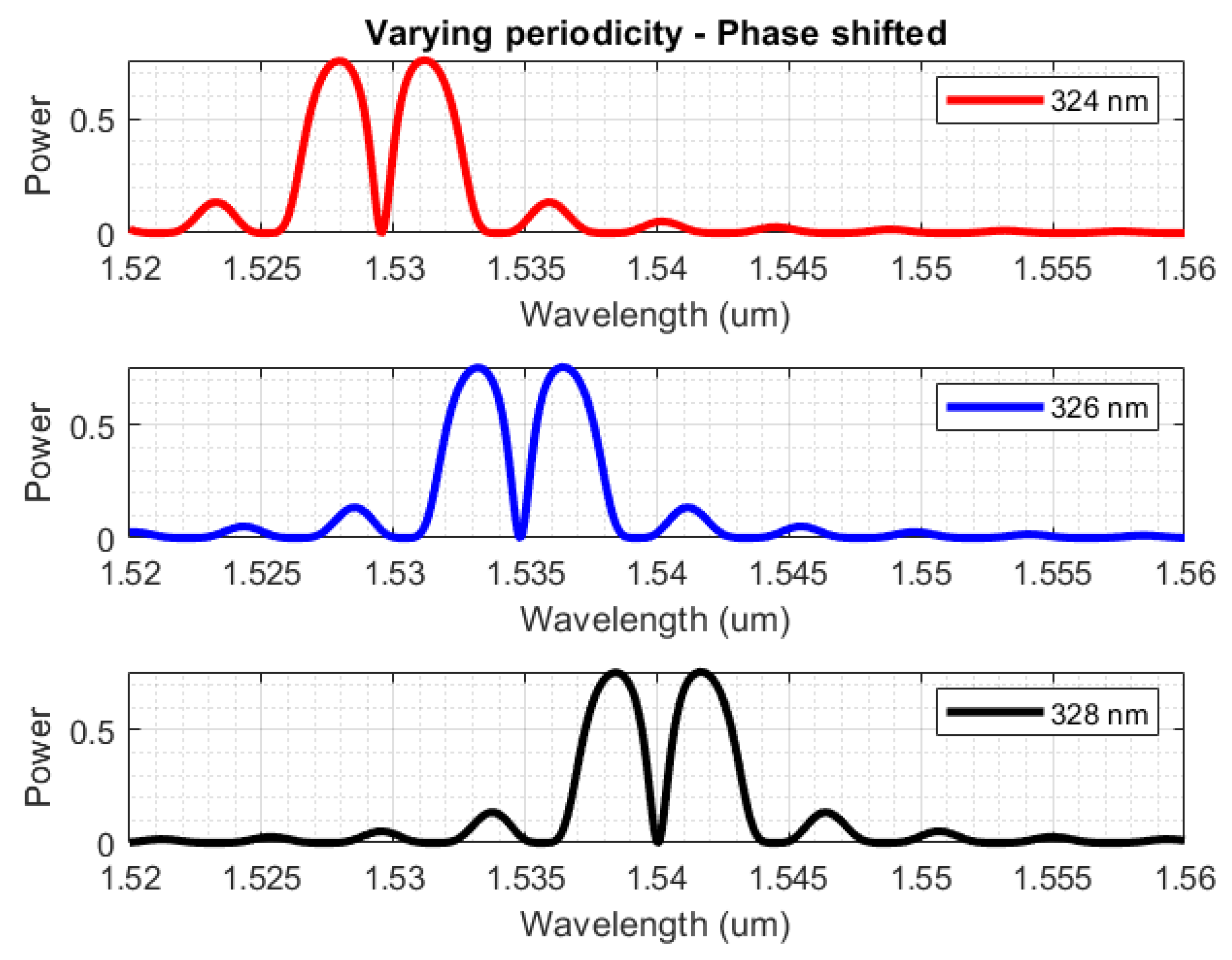
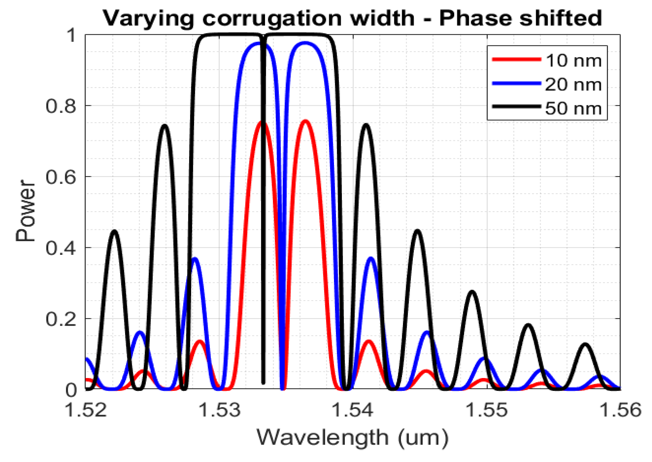
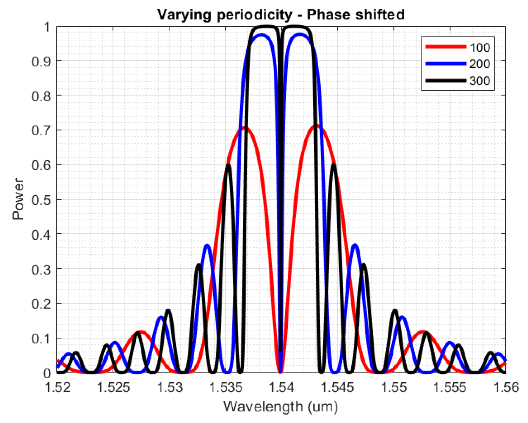
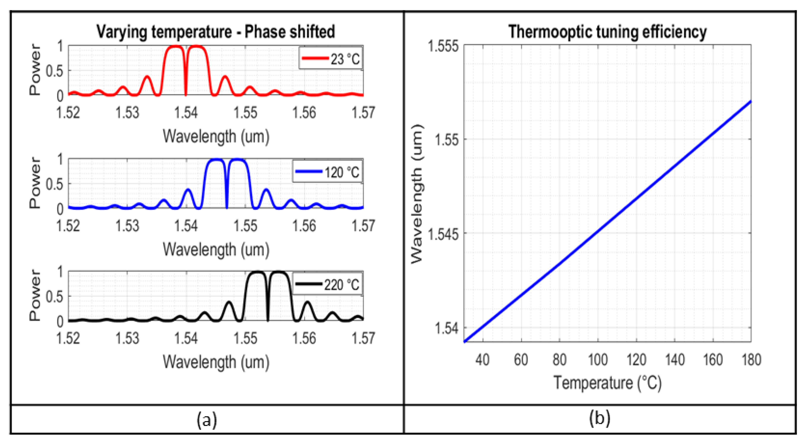
4.1.2. Propagation Simulation Study
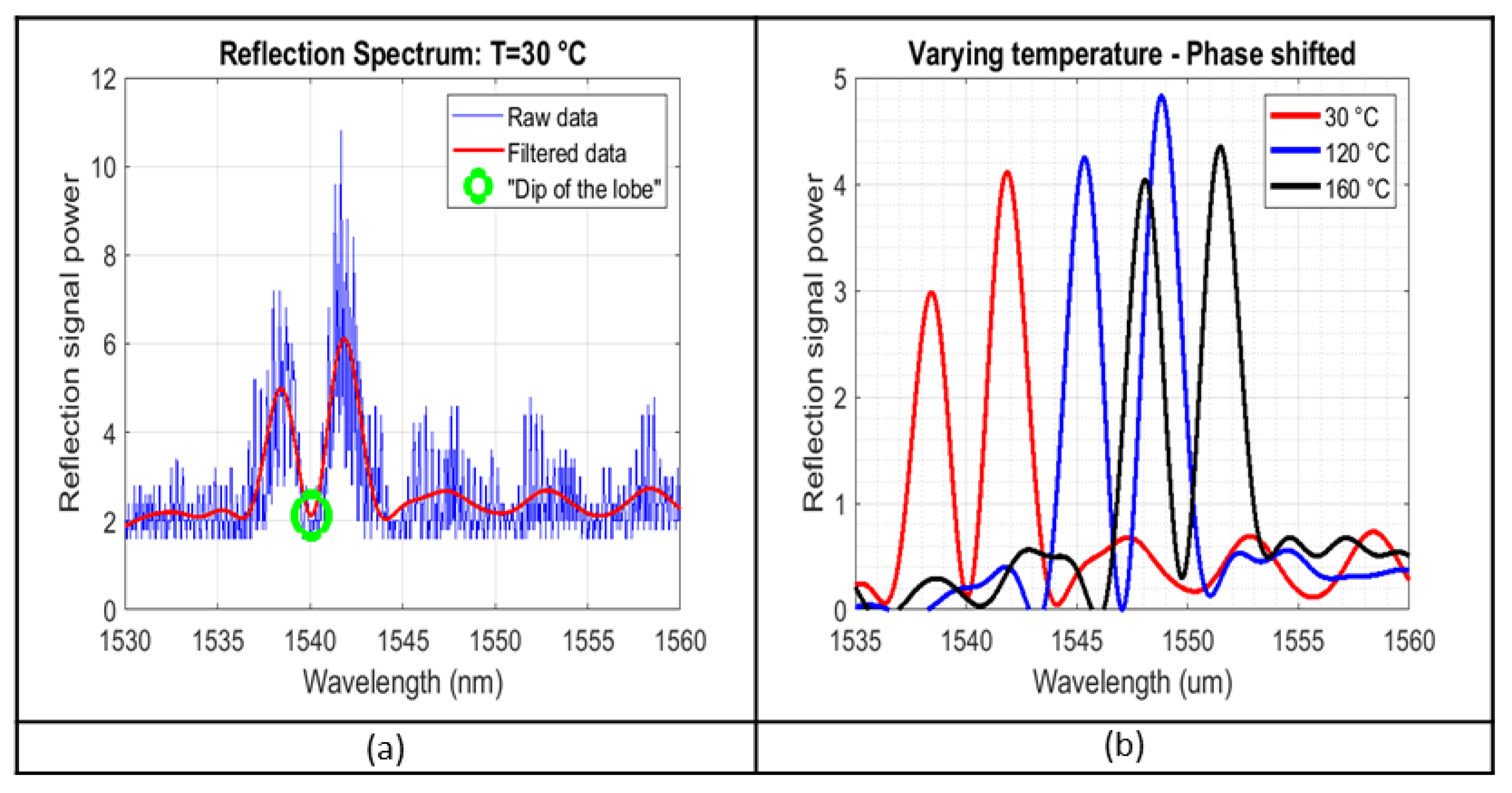
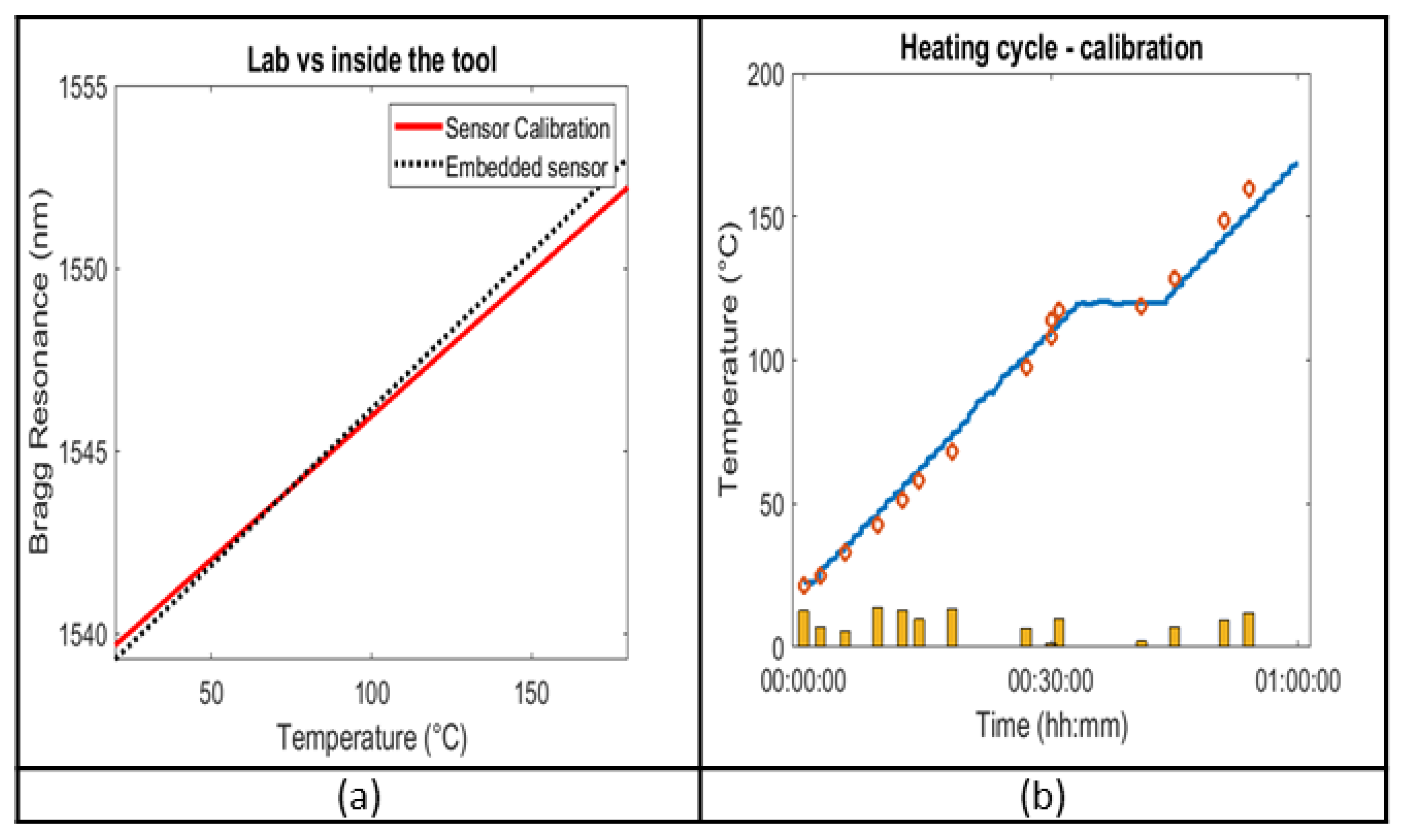
4.2. Experimental Results
5. Conclusions
Author Contributions
Funding
Institutional Review Board Statement
Informed Consent Statement
Data Availability Statement
Conflicts of Interest
References
- Parveez, B.; Kittur, M.I.; Badruddin, I.A.; Kamangar, S.; Hussien, M.; Umarfarooq, M.A. Scientific Advancements in Composite Materials for Aircraft Applications: A Review. Polymers 2022, 14, 5007. [Google Scholar] [CrossRef]
- Chen, Y.; Zhang, J.; Li, Z.; Zhang, H.; Chen, J.; Yang, W.; Yu, T.; Liu, W.; Li, Y. Manufacturing Technology of Lightweight Fiber-Reinforced Composite Structures in Aerospace: Current Situation and toward Intellectualization. Aerospace 2023, 10, 206. [Google Scholar] [CrossRef]
- Ekuase, O.A.; Anjum, N.; Eze, V.O.; Okoli, O.I. A Review on the Out-of-Autoclave Process for Composite Manufacturing. J. Compos. Sci. 2022, 6, 172. [Google Scholar] [CrossRef]
- Bao, Y.; Huang, Y.; Hoehler, M.S.; Chen, G. Review of Fiber Optic Sensors for Structural Fire Engineering. Sensors 2019, 19, 877. [Google Scholar] [CrossRef] [PubMed]
- Wei, C.; Cao, T. A tunable ultrasensitive plasmonic biosensor based on α-MoO3/graphene hybrid architecture. J. Phys. D Appl. Phys. 2021, 54, 234005. [Google Scholar] [CrossRef]
- Wang, Z.; Liu, Y.; Gong, C.; Yuan, Z.; Shen, L.; Chang, P.; Liu, K.; Xu, T.; Jiang, J.; Chen, Y.-C.; et al. Liquid crystal-amplified optofluidic biosensor for ultra-highly sensitive and stable protein assay. PhotoniX 2021, 2, 18. [Google Scholar] [CrossRef] [PubMed]
- Sun, H.; Wang, S.; Hu, X.; Liu, H.; Zhou, X.; Huang, J.; Cheng, X.; Sun, F.; Liu, Y.; Liu, D. Detection of surface defects and subsurface defects of polished optics with multisensor image fusion. PhotoniX 2022, 3, 6. [Google Scholar] [CrossRef]
- Cao, T.; Wang, Z.; Mao, L. Reconfigurable label-free shape-sieving of submicron particles in paired chalcogenide waveguides. Nanoscale 2022, 14, 2465–2474. [Google Scholar] [CrossRef] [PubMed]
- Kinet, D.; Mégret, P.; Goossen, K.W.; Qiu, L.; Heider, D.; Caucheteur, C. Fiber Bragg Grating Sensors toward Structural Health Monitoring in Composite Materials: Challenges and Solutions. Sensors 2014, 14, 7394–7419. [Google Scholar] [CrossRef]
- Ferdinand, P.; Magne, S.; Dewynter-Marty, V.; Rougeault, S.; Maurin, L. Applications of Fiber Bragg Grating Sensors in the Composite Industry. MRS Bull. 2002, 27, 400–407. [Google Scholar] [CrossRef]
- Van Hoe, B.; Lee, G.; Bosman, E.; Missinne, J.; Kalathimekkad, S.; Maskery, O.; Webb, D.J.; Sugden, K.; Van Daele, P.; Van Steenberge, G. Ultra Small Integrated Optical Fiber Sensing System. Sensors 2012, 12, 12052–12069. [Google Scholar] [CrossRef]
- Kazanskiy, N.L.; Khonina, S.N.; Butt, M.A. Advancement in Silicon Integrated Photonics Technologies for Sensing Applications in Near-Infrared and Mid-Infrared Region: A Review. Photonics 2022, 9, 331. [Google Scholar] [CrossRef]
- Harmsma, P.J.; Engelmann, M.J.; Schmits, R.; Westerveld, W.J.; van den Berg, J.H.; Agovic, K.; van Vliet, R.E.; Yousefi, M. Photonic pressure sensor in silicon on insulator. In Proceedings of the CLEO/Europe—EQEC 2009—European Conference on Lasers and Electro-Optics and the European Quantum Electronics Conference, Munich, Germany, 14–19 June 2009; p. 1. [Google Scholar] [CrossRef]
- Xie, S. The Design Considerations and Challenges in MOS-Based Temperature Sensors: A Review. Electronics 2022, 11, 1019. [Google Scholar] [CrossRef]
- Poiana, D.A.; Posada-Roman, J.E.; Garcia-Souto, J.A. Compact Interrogation System of Fiber Bragg Grating Sensors Based on Multiheterodyne Dispersion Interferometry for Dynamic Strain Measurements. Sensors 2022, 22, 3561. [Google Scholar] [CrossRef]
- Poulopoulos, I.; Zervos, C.; Syriopoulos, G.; Missinne, J.; Szaj, M.; Avramopoulos, H. Silicon photonics temperature and refractive index sensor for curing process monitoring in composite material industry. In Optical Sensing and Detection VII; SPIE: Paris, France, 2022; pp. 76–88. [Google Scholar] [CrossRef]
- Syriopoulos, G.; Poulimenos, A.; Poulopoulos, G.; Poulimenou, M.; Missinne, J.; Szaj, M.; Zervos, C.; Van Steenberge, G.; Avramopoulos, H. Demonstration of photonic temperature sensor for RTM-6 composite manufacturing process (180°C) integrated with PMOC system. In Integrated Optics: Devices, Materials, and Technologies XXVII; SPIE: Paris, France, 2023. [Google Scholar] [CrossRef]
- Cheng, L.; Mao, S.; Li, Z.; Han, Y.; Fu, H.Y. Grating Couplers on Silicon Photonics: Design Principles, Emerging Trends and Practical Issues. Micromachines 2020, 11, 666. [Google Scholar] [CrossRef]
- Marchetti, R.; Lacava, C.; Khokhar, A.; Chen, X.; Cristiani, I.; Richardson, D.J.; Reed, G.T.; Petropoulos, P.; Minzioni, P. High-efficiency grating-couplers: Demonstration of a new design strategy. Sci. Rep. 2017, 7, 16670. [Google Scholar] [CrossRef] [PubMed]
- Mangal, N.; Missinne, J.; Van Campenhout, J.; Snyder, B.; Van Steenberge, G. Ball Lens Embedded Through-Package via to Enable Backside Coupling Between Silicon Photonics Interposer and Board-Level Interconnects. J. Light. Technol. 2020, 38, 2360–2369. [Google Scholar] [CrossRef]
- Missinne, J.; Geudens, V.; Van Put, S.; Poulopoulos, G.; Szaj, M.; Syriopoulos, G.; Zervos, C.; Avramopoulos, H.; Van Steenberge, G. A fully packaged silicon photonic Bragg grating temperature sensor with a compact back side interface based on a ball lens. In Silicon Photonics XVIII; SPIE: Paris, France, 2023; pp. 87–96. [Google Scholar] [CrossRef]
- Neale, G.; Skordos, A. Insertion of large diameter through-thickness metallic pins in composites. Mater. Des. 2022, 216, 110559. [Google Scholar] [CrossRef]
- Watanabe, H.; Yamada, N.; Okaji, M. Linear Thermal Expansion Coefficient of Silicon from 293 to 1000 K. Int. J. Thermophys. 2004, 25, 221–236. [Google Scholar] [CrossRef]
- Gallagher, D.F.G.; Felici, T.P. Eigenmode expansion methods for simulation of optical propagation in photonics: Pros and cons. In Integrated Optoelectronics Devices; Sidorin, Y.S., Tervonen, A., Eds.; SPIE: San Jose, CA, USA, 19 June 2003; pp. 69–82. [Google Scholar] [CrossRef]
- Wang, X. Design and Fabrication of Integrated Optical Waveguides and Sidewall Bragg Gratings. Ph.D. Thesis, Texas A & M University, College Station, TX, USA, December 2014. Available online: https://oaktrust.library.tamu.edu/handle/1969.1/153942 (accessed on 24 May 2023).
- Ibrahim, S.K.; Farnan, M.; Karabacak, D.M.; Singer, J.M. Enabling technologies for fiber optic sensing. In Proceedings of the SPIE Photonics Europe, Brussels, Belgium, 3–7 April 2016; Berghmans, F., Mignani, A.G., Eds.; p. 98990Z. [Google Scholar]
- Agrawal, G.P.; Radic, S. Phase-shifted fiber Bragg gratings and their application for wavelength demultiplexing. IEEE Photonics Technol. Lett. 1994, 6, 995–997. [Google Scholar] [CrossRef]
- Komma, J.; Schwarz, C.; Hofmann, G.; Heinert, D.; Nawrodt, R. Thermo-optic coefficient of silicon at 1550 nm and cryogenic temperatures. Appl. Phys. Lett. 2012, 101, 041905. [Google Scholar] [CrossRef]


| Material | Refractive Index |
|---|---|
| Silicon | 3.47 |
| Buried Oxide (BOx) | 1.45 |
| Top Oxide | 1.41 |
| Variable | Effect |
|---|---|
| Corrugation width | ) |
| Grating pitch | ) |
| Number of periods | Affects the peak reflectivity and 3 dB bandwidth [25] |
| a (pm/°C) | b (nm) | ||
|---|---|---|---|
| Calibration | 78.4 | 1538.1 | 0.948 |
| Embedded sensor | 85.8 | 1537.5 | 0.944 |
Disclaimer/Publisher’s Note: The statements, opinions and data contained in all publications are solely those of the individual author(s) and contributor(s) and not of MDPI and/or the editor(s). MDPI and/or the editor(s) disclaim responsibility for any injury to people or property resulting from any ideas, methods, instructions or products referred to in the content. |
© 2023 by the authors. Licensee MDPI, Basel, Switzerland. This article is an open access article distributed under the terms and conditions of the Creative Commons Attribution (CC BY) license (https://creativecommons.org/licenses/by/4.0/).
Share and Cite
Syriopoulos, G.; Poulopoulos, I.; Zervos, C.; Kyriazi, E.; Poulimenos, A.; Szaj, M.; Missinne, J.; van Steenberge, G.; Avramopoulos, H. Photonic Integrated Circuit Based Temperature Sensor for Out-of-Autoclave Composite Parts Production Monitoring. Sensors 2023, 23, 7765. https://doi.org/10.3390/s23187765
Syriopoulos G, Poulopoulos I, Zervos C, Kyriazi E, Poulimenos A, Szaj M, Missinne J, van Steenberge G, Avramopoulos H. Photonic Integrated Circuit Based Temperature Sensor for Out-of-Autoclave Composite Parts Production Monitoring. Sensors. 2023; 23(18):7765. https://doi.org/10.3390/s23187765
Chicago/Turabian StyleSyriopoulos, Georgios, Ioannis Poulopoulos, Charalampos Zervos, Evrydiki Kyriazi, Aggelos Poulimenos, Michal Szaj, Jeroen Missinne, Geert van Steenberge, and Hercules Avramopoulos. 2023. "Photonic Integrated Circuit Based Temperature Sensor for Out-of-Autoclave Composite Parts Production Monitoring" Sensors 23, no. 18: 7765. https://doi.org/10.3390/s23187765