Article

Preparation of Hybrid Films Based in Aluminum 8-Hydroxyquinoline as Organic Semiconductor for Photoconductor Applications

by
María Elena Sánchez Vergara
1,*,
Luis Alberto Cantera Cantera
1,
Citlalli Rios
2,
Roberto Salcedo
2,
Octavio Lozada Flores
3 and
Ateet Dutt
2
1
Facultad de Ingeniería, Universidad Anáhuac México, Avenida Universidad Anáhuac 46, Col. Lomas Anáhuac, Huixquilucan 52786, Estado de México, Mexico
2
Instituto de Investigaciones en Materiales, Universidad Nacional Autónoma de México, Circuito Exterior s/n. C.U., Mexico City 04510, Mexico
3
Facultad de Ingeniería, Universidad Panamericana, Augusto Rodin 498, Insurgentes Mixcoac, Mexico City 03920, Mexico
*
Author to whom correspondence should be addressed.
Sensors 2023, 23(18), 7708; https://doi.org/10.3390/s23187708
Submission received: 8 July 2023 / Revised: 24 August 2023 / Accepted: 1 September 2023 / Published: 6 September 2023

Abstract

:
In the present work, we have investigated an organic semiconductor based on tris(8-hydroxyquinoline) aluminum (AlQ3) doped with tetracyanoquinodimethane (TCNQ), which can be used as an organic photoconductor. DFT calculations were carried out to optimize the structure of semiconductor species and to obtain related constants in order to compare experimental and theoretical results. Subsequently, AlQ3-TCNQ films with polypyrrole (Ppy) matrix were fabricated, and they were morphologically and mechanically characterized by Scanning Electron Microscopy, X-ray diffraction and Atomic Force Microscopy techniques. The maximum stress for the film is 8.66 MPa, and the Knoop hardness is 0.0311. The optical behavior of the film was also analyzed, and the optical properties were found to exhibit two indirect transitions at 2.58 and 3.06 eV. Additionally, photoluminescence measurements were carried out and the film showed an intense visible emission in the visible region. Finally, a photoconductor was fabricated and electrically characterized. Applying a cubic spline approximation to fit cubic polynomials to the J-V curves, the ohmic to SCLC transition voltage V ON and the trap-filled-limit voltage V TFL for the device were obtained. Then, the free carrier density and trap density for the device were approximated to n 0 = 4.4586 × 10 19 1 m 3 and N t = 3.1333 × 10 31 1 m 3 , respectively.

Graphical Abstract

1. Introduction

The development of optoelectronic and photovoltaic devices based on organic semiconductors has drawn attention due to their promising applications [1,2,3]. Specifically, an organic optocoupler (OOC) consists of three main components: an organic photoemitter, an insulator and an organic photodetector [4]. Such an organic photodetector, also known as a photosensor, can be divided into organic photoresistors, organic photodiodes or organic phototransistors [4,5]. These organic semiconductor devices possess a photoconductive effect, which modifies their conductivity due to the incidence of light; i.e., when a voltage is applied, a current flows and the incident light on the device will cause an increase in this current [6,7]. The current flowing in a semiconductor in the absence of some kind of light is called dark current, whereas the flowing current produced by an incident light is called photon-induced current or photocurrent [7]. When an organic semiconductor exhibits the photoconductive effect, it may be classified as an organic photoconductor (OPC) [4,7].
Organic semiconductors require a conjugated structure to participate effectively in electric conductivity [1,2]. The surface of their π orbitals should stabilize the electronic charge by resonant effect and facilitate intermolecular interactions by overlapping orbitals. For this reason, the correct selection of the organic base structure is a determining aspect in the design of new organic semiconductors. Small π-conjugated molecules are excellent candidates for assembling different types of organic semiconductors due to their attractive features, such as well-defined chemical structure, easily modified structural layouts, fine-tuning of their energy levels and excellent reproducibility [8,9,10,11,12]. Small π-conjugated molecules can be processed in solution [11]; besides, due to their low molecular weight [8,13], they can also be deposited by vacuum thermal evaporation for assembling ordered layers that improve the performance of the final device. Vacuum thermal deposition allows to produce devices with controlled multilayers and stability ideal for commercialization. However, small π-conjugated molecules with sufficiently high thermal stability and better light harvesting capability are required [13]. For this reason, solution deposition methods are also used in processing small molecules either in solution or dispersion [14,15,16,17]. This latter feature provides several advantages, such as the possibility of preparing thin films with insoluble molecules showing high chemical stability, which, when forming part of photovoltaic and optoelectronic devices, will enhance their performance without degrading easily.
Metal quinolines (MQs) are small molecules that have been used in organic optoelectronic devices [18,19,20,21,22] due to their ability to form thin films in solution [18,23,24,25] and by evaporation [19,22,26,27] since they exhibit high chemical and thermal stability. MQs also offer easy color tunability with simple synthesis [28,29,30,31], magnetism properties [32] and electron transport behavior [23,28,33]. Moreover, the fluorescence of MQs has led to their classification as an important class of electro-luminescent/electron transport materials [23]. It is also known that changing the central metal ion affects the luminescence peak position of the MQs [18,20,21,22,23,34]. Above the MQs family, tris(8-hydroxyquinoline) aluminum (Alq3) is the most popular MQs semiconductor due to its strong luminesce, high electron mobility and, in addition, due to its low cost and simple technology of fabrication [26,35]. Alq3 is a small molecule with conjugated π-electron systems and has a non-centrosymmetric crystal structure [35] with ∝, β, γ, δ and ε crystalline phases [35,36,37,38,39]. Alq3 has become used to fabricate thin films by both the solution process and by using vacuum thermal deposition [26,39]; therefore, a considerable number of studies are focused on the nucleation and growth of Alq3 films [40], as well as on their surface topography [41], their optical properties and their energy band gap under indirect and direct conditions [26]. Additionally, it should be considered that many studies have investigated the applications of Alq3 films on organic light-emitting devices (OLEDs) [24,35,42], display devices and systems [43] and organic photovoltaic cells [44]. However, only a few studies have been devoted to understanding the current–voltage characteristics in order to manipulate doping and improve the performance of Alq3, the latest mainly focusing on electrical conduction mechanism analysis, such as transition from ohmic to space-charge-limited current (SCLC) regimes [45,46], as well as on the estimation of electrical parameters, such as trap factors, free carrier density, ohmic to SCLC transition voltage and trap-filled-limit voltage [47,48,49].
Although space-charge-limited current theory dates to the 1940s through the work of Mott and Gurney [50], the study of ohmic and space-charge-limited currents in semiconductors is the most widely used to explain the mechanisms of charge transport and carrier trapping. In the case of the SCLC regime, it takes place when the electrode injects more carriers than those the material can transport and is modeled by a quadratic equation. On the other hand, the ohmic regime exhibits a linear behavior that arises when the amount of injection is low compared to thermally generated carriers and impurities [45,46].
The present work aims to employ Alq3 as a small molecule to produce active layers of a photoconductor device showing a one-layer structure formed by Alq3 doped with tetracyanoquinodimethane (Alq3-TCNQ). TCNQ is an electronic acceptor capable of forming stable radicals, with valence electrons located above and below the median plane of the molecule in delocalized π orbitals [51,52]. TCNQ favors the formation of molecular anisotropic blocks, where conduction channels are generated. Subsequently, the Alq3-TCNQ-doped semiconductor was embedded in a polypyrrole (Ppy) polymeric matrix to fabricate a hybrid active layer with a dispersed heterojunction architecture. In this layer, there is high surface contact between Alq3-TCNQ and the Ppy matrix, which favors the dissociation of excitons. Furthermore, Ppy was chosen due to its conductive properties and moderate band gap caused by its heteroatoms and π-conjugated system [53]. Ppy possesses a unique combination of environmental stability and structural versatility that allows it to be used as a matrix in the fabrication of heterojunction hybrid films. The (Alq3-TCNQ):Ppy film was structurally and morphologically characterized, and its optical properties were also evaluated. With respect to the theoretical calculations, a DFT method was used to optimize the structure of Alq3-TCNQ semiconductor complexes; their IR spectra were calculated and compared to those experimentally obtained. Additionally, their frontier molecular orbitals were determined, and the corresponding bandgap values were calculated with these results. Finally, a simple device was fabricated with the hybrid film, and their electrical characteristics were investigated by current-voltage (I-V) measurements under different lighting conditions. The motivation to study the electrical behavior of (Alq3-TCNQ):Ppy hybrid films under different lighting conditions is related to determining whether their optical properties affect the amount of electric current transported through this film. The theoretical model can explain the conduction mechanisms in the device. Also, based on the current-voltage measurements of the device and its approximation by cubic splines, the ohmic to SCLC transition voltage V ON and the trap-filled-limit voltage V TFL were obtained.

2. Theoretical Calculations

The structural characterization of the parent molecules Alq3 and TCNQ and the Alq3-TCNQ semiconductor was carried out using the B3PW91 hybrid method contained in Gaussian 16 Package [54] and the 6-31G basis set. The method combines Becke’s gradient corrections [55] for exchange and Perdew–Wang’s for correlation [56]. Frequency calculations were carried out at the same level of theory in order to confirm that the optimized structures were at the minimum of the potential energy surface.

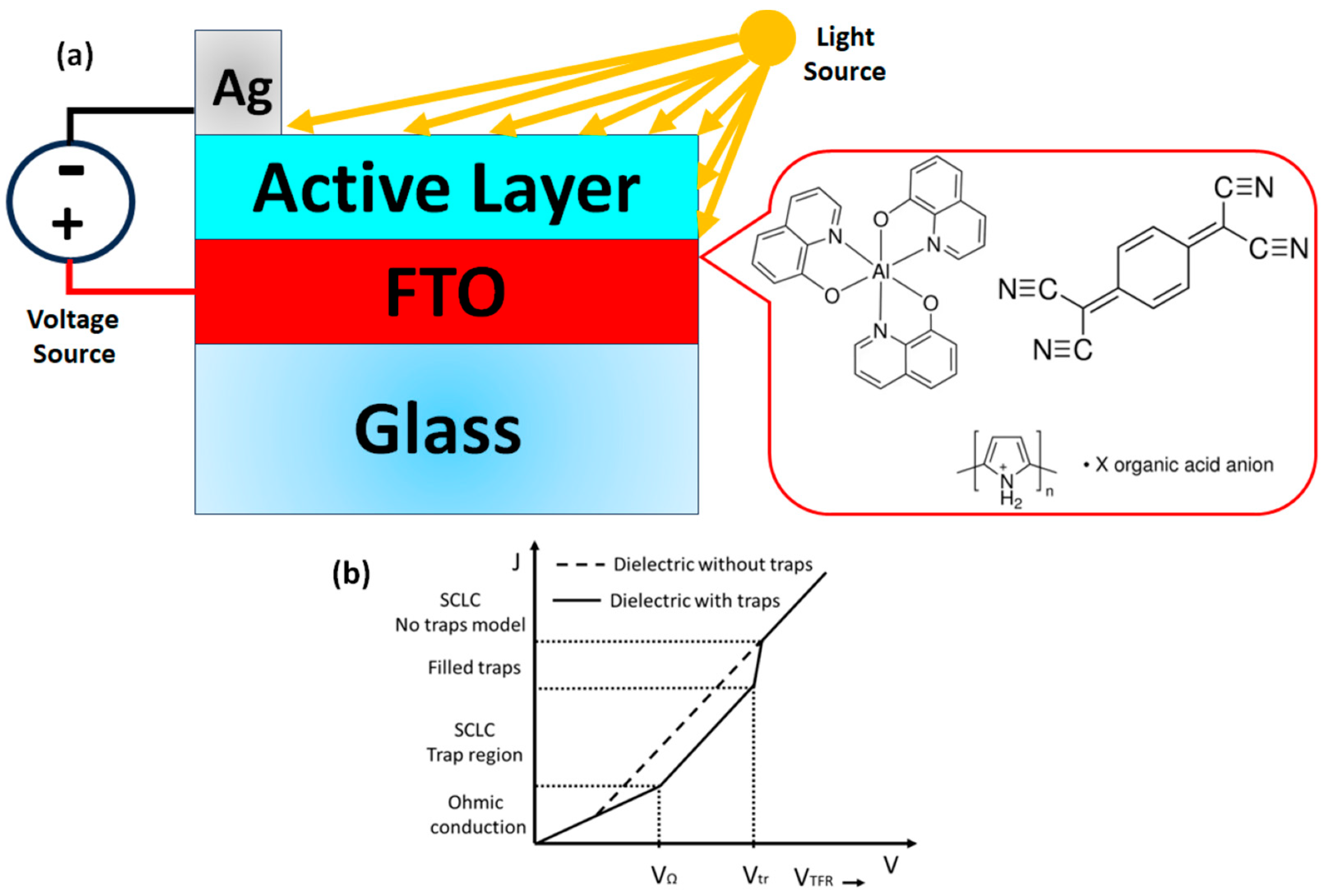
3. Materials and Methods

Tris-(8-hydroxyquinoline)aluminum (Alq3; C27H18AlN3O3), 7,7,8,8-tetracyanoquinodimethane (TCNQ; C12H4N4) and polypyrrole (Ppy) were obtained from Sigma Aldrich (Sigma-Aldrich, St. Louis, MO, USA) and required no further purification. Afterwards, an Alq3-TCNQ-doped semiconductor was obtained by the dissolution of 106 mg (0.3 mmol) of Alq3 and 102 mg (0.5 mmol) of TCNQ in 20 mL of ethanol. Doping was carried out for 30 min at 425 K in a heated reactor Monowave 50 (Anton Paar México, S.A. de C.V. Hidalgo, México) with a pressure sensor. The reactor is operated with a borosilicate glass vial and manually closed by a cover with an integrated pressure (0–20 bar) and temperature sensor. The system was cooled and brought to atmospheric pressure; the Alq3-TCNQ was filtered, washed with ethanol and dried in a vacuum. The Alq3-TCNQ semiconductor was subsequently deposited on Ppy to form a composite film onto different substrates: glass, high-resistivity monocrystalline n-type silicon wafers (c-Si) and coated glass slides with Fluorine-Tin-Oxide (FTO). The glass and FTO substrates were previously cut and washed consecutively in an ultrasonic bath with chloroform, ethanol and acetone solvents. The silicon substrates, however, were cut and later washed with “p” solution (10 mL HF, 15 mL HNO3 and 300 mL H2O). The film was fabricated from a simple dispersion with 5 mL of the Ppy and Alq3-TCNQ from a dilution of 10 wt% in p-cresol. The distribution Alq3-TCNQ with Ppy was dispersed using the G560 shaker of Scientific Industries Vortex-Genie (Bohemia, NY, USA). A syringe was used to apply 0.6 mL on the substrate surface to obtain the films and then spread the dispersion. Subsequently, the films were brought to 55 °C for 5 min in the drying oven Briteg SC-92898 (Briteg Instrumentos Científicos, S.A de C.V. Mexico City, Mexico). The last accelerated the film fabrication and prevented the samples from swelling and cracking during drying. An FTIR spectroscopy analysis was performed to verify the main functional groups of the Alq3-TCNQ semiconductor using a Nicolet iS5-FT spectrometer (Thermo Fisher Scientific Inc., Waltham, MA, USA) . Morphological and topographical characteristics were, respectively, investigated with a ZEISS EVO LS 10 scanning electron microscope (SEM, Carl Zeiss AG. Jena, Germany) and with a Nano AFM atomic force microscope (AFM, Nanosurf AG, Liesta, Switzerland) using a Ntegra platform for the (Alq3-TCNQ):Ppy films deposited on both glass and silicon substrates. Additionally, the films on glass were examined by X-ray diffraction analysis (XRD) using the θ–2θ technique in a Rigaku Miniflex 600 diffractometer (Rigau Corporation, Tokyo, Japan) with Cu Kα (λ = 1.5406 Å) at 40 kV, 20 mA. Thickness measurements were carried out using the ZIGO-NEXVIEW profilometry technique. The UV-Vis spectra in glass films were obtained in the 200-1100 nm wavelength range using a UV-Vis 300 Unicam spectrophotometer (Thermo Fisher Scientific Inc., Waltham, MA, USA). Photoluminescence measurements were carried out using He-Cd 325 nm laser (Kimmon Koha Co., Ltd., Tokyo, Japan) at room temperature on an optical table. Finally, the electrical behavior was procured through current–voltage (I-V) measurements in a Keithley 4200-SCS-PK1 auto-ranging pico-ammeter (Tektronix Inc., Beaverton, OR, USA). The evaluation was performed on the FTO/(Alq3-TCNQ):Ppy/Ag device (Figure 1a); Ag was deposited on top of the layers to act as a cathode, and the FTO acted as anode. I-V curves were obtained under darkness, white, red, orange, yellow, green, blue and ultraviolet lights in a range of −1.2 to 1.2 V at room temperature. The principal studies of the current-voltage (I-V) characteristics in semiconductors are the ohmic and space-charge-limited currents (SCLC); therefore, several investigations, such as [45,46,57,58,59], have identified a typical current density-voltage curve, as shown in Figure 1b.
Two regimes can be identified in Figure 1b; the first one is the ohmic regime at low voltages that can be expressed by
J Ω = q n 0 μ n V d s ,
when the voltage is increased, the second regime is quadratic, called the space-charge-limited current (SCLC) regime, defined by
J SCLC = 9 8 μ n ε 0 ε r V 2 d s 3 ,
where J denotes the current density, q is the electronic charge, n 0 is the free carrier density, μ n is the electron mobility, V is the applied voltage, d s is the thickness of the sample, ε 0 is the vacuum permittivity and ε r is the dielectric constant. Generally, a SCLC regime also occurs at high voltages but with a higher growth rate than the quadratic regime. In addition to the ohmic and SCLC regimes, it has been identified the ohmic to SCLC transition voltage denoted by V ON , and the trap-filled-limit voltage denoted by V TFL determines the change from one quadratic regime to another. These transition voltages are defined by
V ON = 8 9 q n 0 ε 0 ε r d s 2 ,
V TFL = q N t 2 ε r d s 2 ,
where N t is the trap density. Notice that, when the transition voltages are determined from Equations (3) and (4), the free carrier density and the trap density can be calculated.

4. Results and Discussion

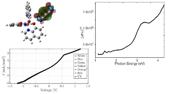
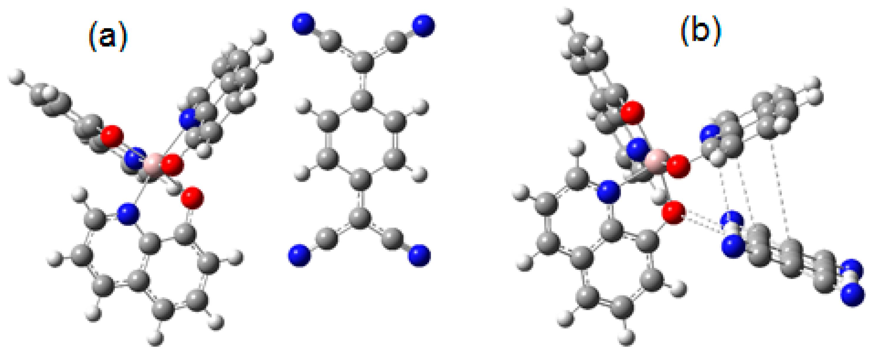
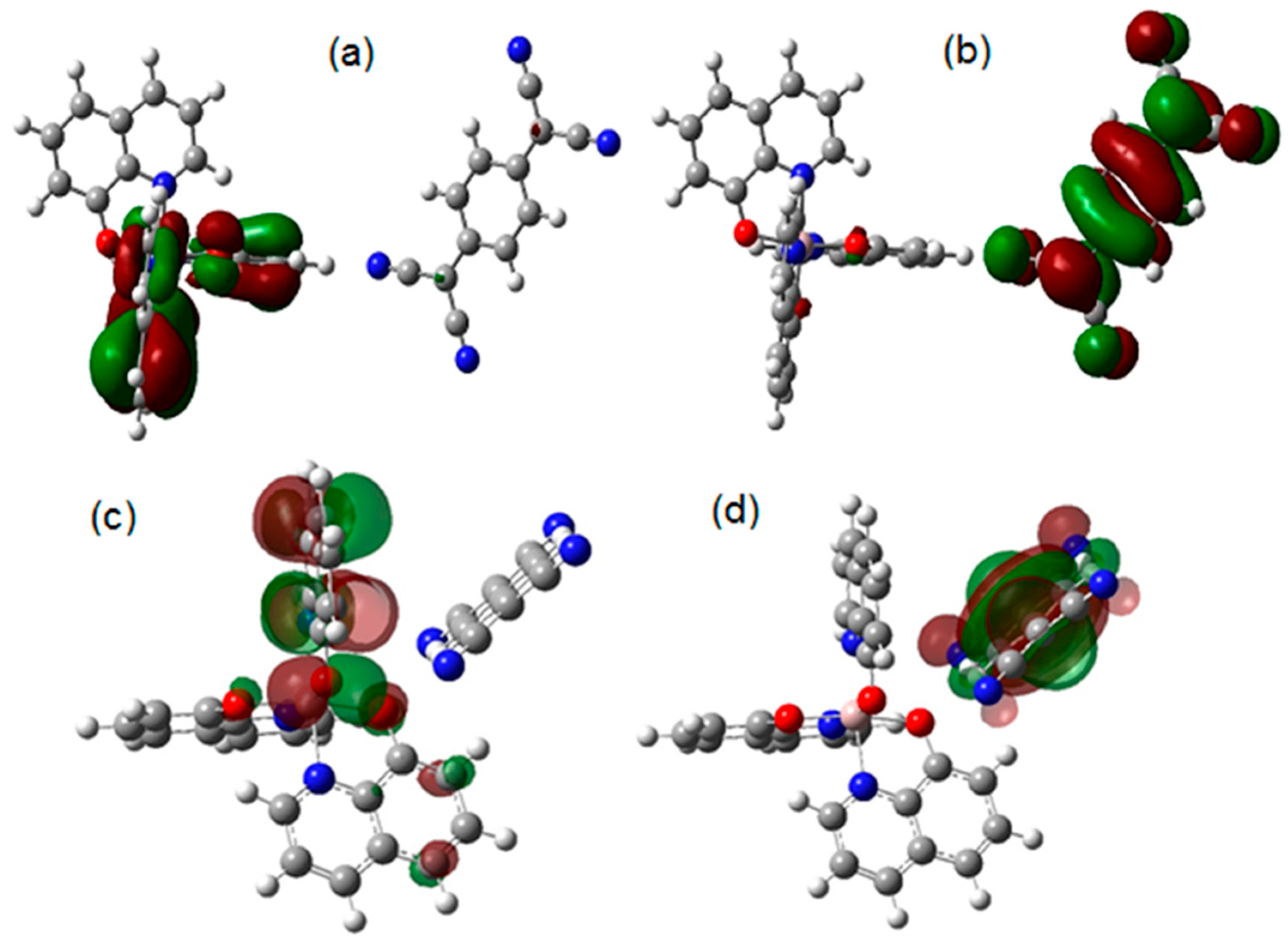
4.1. DFT Calculations

To determine the feasibility of doping the electronic donor Alq3 with the electronic acceptor TCNQ, the molecular geometry of both precursor compounds and the organic semiconductor was optimized by using the DFT method. The energy values of the molecular orbitals HOMO (highest occupied molecular orbital) and LUMO (lowest unoccupied molecular orbital) for hydroxyquinoline Alq3 are −5.1 and −1.95 eV, respectively, and the band gap value is 3.15 eV. These results are in the same order of magnitude as those calculated by Sevgili et al. [24] for aluminum 8-hydroxyquinoline microbelts and microdots. For the TCNQ, the calculated HOMO value is −7.45 eV, the LUMO has a value of −4.95 eV and the bandgap is 2.5 eV. It should be considered that the band gaps obtained for both precursor species are significant to be considered efficient organic semiconductors. The control of the HOMO–LUMO energy gap of organic semiconductors is fundamental for the effective transport of charges. To understand the interaction between hydroxyquinoline and TCNQ, two possibilities were studied. The first one considers the interaction between central oxygens of hydroxyquinoline and the aromatic ring of TCNQ (Hal-TCNQ1). In a second case, the interaction between the hydrogen atoms of one of the rings of hydroxyquinoline and the nitrogen atoms of TCNQ (Hal-TCNQ2) was studied. These two interactions are the unique stable possibilities of dispersion forces interactions and are hydrogen bonds. Figure 2 shows the optimized structures of the mentioned cases, and the mentioned hydrogen bonds are clearly demonstrated.
Figure 3a,b show the frontier molecular orbitals for Hal-TCNQ1; HOMO is located over hydroxyquinoline and LUMO over TCNQ; this result was expected because TCNQ is known for being an excellent electron acceptor [60]. The donor–acceptor behavior of the species is the source of the interaction between them; the HOMO and LUMO values are 5.14 and 4.87 eV, respectively, and the band gap value yields 0.271 eV. In order to measure the importance of the interaction between the molecules, the Wiberg index was calculated. Table 1 shows the distance between the interacting atoms and the Wiberg index values. The calculations showed that three hydrogen bonds were formed between hydrogen atoms of hydroxyquinoline and TCNQ. On the other hand, Figure 3c,d show the frontier molecular orbitals of Hal-TCNQ2; again, HOMO is located over hydroxyquinoline and LUMO over TCNQ. In this case, HOMO yields 5.44 eV and LUMO 4.47 eV, whereas the band gap value is 0.968 eV. Again, the Wiberg index was calculated to analyze the interaction between atoms. Three hydrogen bridges were localized; Table 1 shows the distance and the Wiberg index for the involved atoms. It is observed that, for the interaction O(51)-H(70), the Wiberg index is an order of magnitude higher and exhibits the smallest distance; thus, this is the main bond leading the interaction. Based on the information, it is possible to conclude that both molecules constitute an electronic complex by means of hydrogen bonds, its energy gap decreases and the semiconductor behavior is notably improved with the formation of this complex. An explanation for this behavior is that the intermolecular interaction (the hydrogen bond) directly arises from the HOMO of hydroxyquinoline and the LUMO of TCNQ, whose energy values are very close.
It is important to consider that the values of 0.271 and 0.968 eV for Hal-TCNQ1 and Hal-TCNQ2 correspond to low band gap semiconductors [61,62]. Apparently, the donor-acceptor approach introduced by Havinga et al. [62] is the cause of the significant decrease in the band gap value. The position of the HOMO and LUMO levels and the band gap of the resulting doped semiconductor are determined by the hybridization of the corresponding frontier orbitals of the Alq3 and TCNQ units (see Figure 3). Therefore, based on the DFT calculations, carrying out the experimental doping of Alq3 with TCNQ is convenient. Additionally, the IR spectra were theoretically obtained for both HAl-TCNQ1 and hAl-TCNQ2 (see Figure 4), and the results provide a hint of the feasibility of carrying out the experimental doping of the semiconductor Alq3-TCNQ.

4.2. Fabrication and Characterization of Hybrid Film

After the doping, the Alq3-TCNQ was characterized by IR spectroscopy in the KBr pellet. The results were compared to those theoretically obtained; both spectra are shown in Figure 4. Characteristic peaks of Alq3 bands at 400–650 cm−1 can be related to the stretching vibration of the metal ion with the attached ligand, while the peak at 1582 cm−1 is associated with the quinoline group of Alq3 [21,63,64,65,66]; additionally, aromatic stretching C=C (1607 cm−1) is observed in the spectrum. C-C (1469 cm−1) and C-C-H bending vibrations (1169 cm−1) are also present, while peaks at 781 and 646 cm−1 are associated with in-plane ring deformations [21,63]. On the side of the TCNQ dopant, the signal is observed at 2215 cm−1, referring to the CN-stretching mode of the cyano groups [67]. A more detailed analysis is presented in Table 2 to further understand the spectra. The good agreement between the experimental IR spectrum and that theoretically obtained indicates that the calculations yield an excellent approach to the experimental study. However, the hAl-TCNQ2 IR spectrum seems to be more similar to that experimentally obtained. The observed differences between experimental and theoretical spectra are mainly attributed to the conditions established for DFT calculations; indeed, only the interaction between a hydroxyquinoline molecule and a TCNQ molecule as isolated species is considered; i.e., there is no other kind of interaction either with similar molecules or with impurities; thus, this spectrum is very clean with respect to its experimental counterpart. The multiple interactions between Alq3 molecules and their dopant are reflected in the experimental spectrum; such interactions cause both bathochromic and hypsochromic shifts. An IR spectrum of (Alq3-TCNQ): Ppy film was carried out to verify that, after preparing the hybrid film, the doped semiconductor suffered no degradation. The results are shown in Table 2. As expected, no degradation was found.
SEM analysis was carried out to analyze the morphology of the (Alq3-TCNQ):Ppy film, and Figure 5a shows the 250× microphotography of the hybrid film. As can be seen, the film is made up of clusters of various sizes that are distributed along the entire surface. It is a heterogeneous film regarding the shape and size of the clusters formed. The XRD pattern of (Alq3-TCNQ):Ppy film is shown in Figure 5b and exhibits apparent broad diffused diffraction reflections at 2θ regions of 16–38°. No sharp Bragg peaks that could be related to a crystalline structure were presented. This indicates that the clusters assembled in the film and the film itself (see Figure 5a) are essentially amorphous. To complement the information, the (Alq3-TCNQ):Ppy film was studied by AFM, and, as observed in Figure 5c, an irregular topography integrated by crests and valleys of different sizes is presented. This topography is reflected in a root mean square (RMS) of 23.04 nm and an arithmetic mean roughness (Ra) of 15.03 nm. Moreover, considering a maximum applied force of 990 N, the mechanical properties of the hybrid film are (i) the unitary deformation (ε) = 0.744, (ii) the maximum stress (σmax) = 8.66 mPa and (iii) the Knoop microhardness (HK) = 0.0311. One of the most important features for applications in organic optoelectronic devices is high mechanical resistance, which, according to the obtained results, is exhibited by (Alq3-TCNQ):Ppy film.

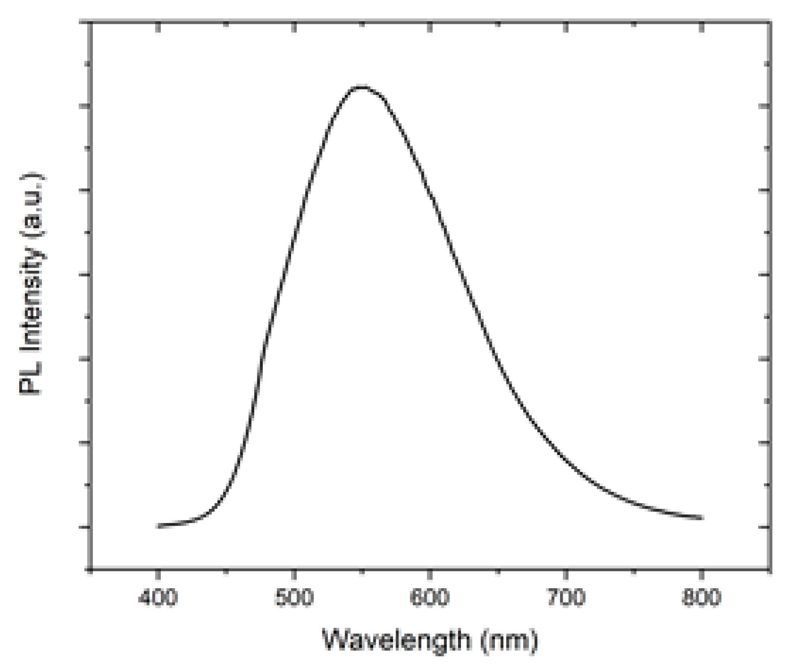
4.3. Optical Characterization of the Device

Aside from controlled band gap, active materials for electronic and photonic applications should demonstrate appropriate absorption and/or emission properties, highest occupied and lowest unoccupied molecular orbital energy levels and charge transport properties. The UV-Vis spectra of the semiconductor film are shown in Figure 6. When the purpose is to use the (Alq3-TCNQ):Ppy film in optoelectronic and photovoltaic devices, then a deep understanding of its optical behavior is required. Figure 6a,b show the absorbance and transmittance, respectively, for the films. In the absorbance spectrum of Alq3-TCNQ film, an absorption band of 375 nm is observed. It has been found that this energy absorption is due to the electron transition from the HOMO in the Alq3 to the LUMO in the TCNQ [22]. In another context, an observed small band at 860 nm is also due to charge transfer with TCNQ. Regarding transmittance, the bands in the film become more noticeable and appear in the 570 to 800 regions. Another feature to highlight in the spectrum of Figure 6b is the high transmittance at a larger wavelength of λ > 900 nm; the transparency of around 80% at high wavelengths coincides with that obtained for both the Alq3 precursor [24] and other hydroxyquinolines, such as zinc [22]. Apparently, despite being doped and embedded in a polymeric matrix, hydroxyquinoline does not lose its transparency at high wavelengths.
The optical band gap is the most relevant parameter to evaluate the potential of (Alq3-TCNQ):Ppy film for optoelectronic devices as active layers. In this work, the optical band gap (Egopt) was calculated through Tauc’s semi-empirical model [68]. Such a method is based on the relation [68,69] α h ν = B ( h ν E g o p t   ) n , where h is Planck’s constant, B is a parameter that depends on the probability of transition, E g o p t   is the optical band gap and n is a number that characterizes the transition process, where n = 2 for indirect allowed transitions. The absorption coefficient (α) and frequency ( ν ) are experimentally obtained from α = l n T / d and ν = c λ , respectively. In these expressions, T is the transmittance, d is the thickness of the film, c is the speed of light and λ is the wavelength. The thickness of 8500 Å was measured by profilometry. The dependence of ( α h ν ) n on h ν was plotted and Egopt was evaluated from the x-axis intercept at (αhν)1/2 = 0. The values of E g o p t   calculated for the films are shown in Figure 6c. The (Alq3-TCNQ):Ppy shows two transitions; the first one at 2.58 eV is the onset gap (Egonset) and the second one at 3.06 eV corresponds to the optical gap (Egopt) [70]. This first transition corresponds to a bound electron–hole pair’s optical absorption and formation (Frenkel exciton) [69,70,71]. The second transition is the energy gap between the valence band (π-band) and the conduction band (π*-band) [71]. The electronic transitions from π to π* explain Egonset and Egopt as a consequence of several factors, including defects, film morphology, structural disorder and traps. However, the obtained value of 2.58 eV is less than the band gaps from 2.66 to 2.84 eV for pristine Alq3 [22,24,26]; it is also less than 3.97 eV for ZnO-doped Alq3 [18] and 3.2 eV for Alq3 doped with sexithiophene [72]. The presence of TCNQ and Ppy decreases the optical gap and also generates the onset gap, which is an indication of a more efficient semiconductor behavior in the (Alq3-TCNQ):Ppy film with respect to other semiconductors derived from Alq3, such as the ones mentioned above.
On the other hand, the Urbach energy (EU) can be used to determine the defects in the band gap and can be determined according to the equation [73,74] α = A a e x p h v E U , where, in addition to the parameters defined above, Aa is a constant of the material that corresponds to the α at the energy gap. The exponential absorption edge can be interpreted as due to the exponential distribution of local states in the energy band gap [73]. Figure 6d displays the linear relation between ln(α) and hν for the hybrid films. The value of the EU was determined from the reciprocal of the slope from this linear relation, and, in this case, it is 0.717 eV. Considering that EU is zero in a perfect semiconductor, the obtained value is high due to the bulk heterojunction between hydroxyquinoline, its dopant and the polymer. However, the interconnections between these three components of the hybrid film can generate charge transport both at the edges of Alq3 and the TCNQ and at the interface of the (Alq3-TCNQ):Ppy film with the electrodes, where charges are less common and efficient when evaluating their electrical behavior. The number of satisfactorily dissociated charges depends on the magnitude of the internal field generated and is limited by the charge mobility of each material.
After studying the band gap, a photoluminescence (PL) analysis of the sample was carried out at room temperature (see Figure 7). It can be seen that, after exciting with a 325 nm laser (UV), the sample shows an intense visible emission in the visible region, with a maximum at around 550 nm. Other groups have observed similar tendencies for the fluorescence or PL of 8-Hydroxyquinoline and their derivatives [75]. A higher intensity of these samples has been attributed to longer alkyl chains, and the mechanism can be mainly attributed to excited state proton transfer (ESPT).

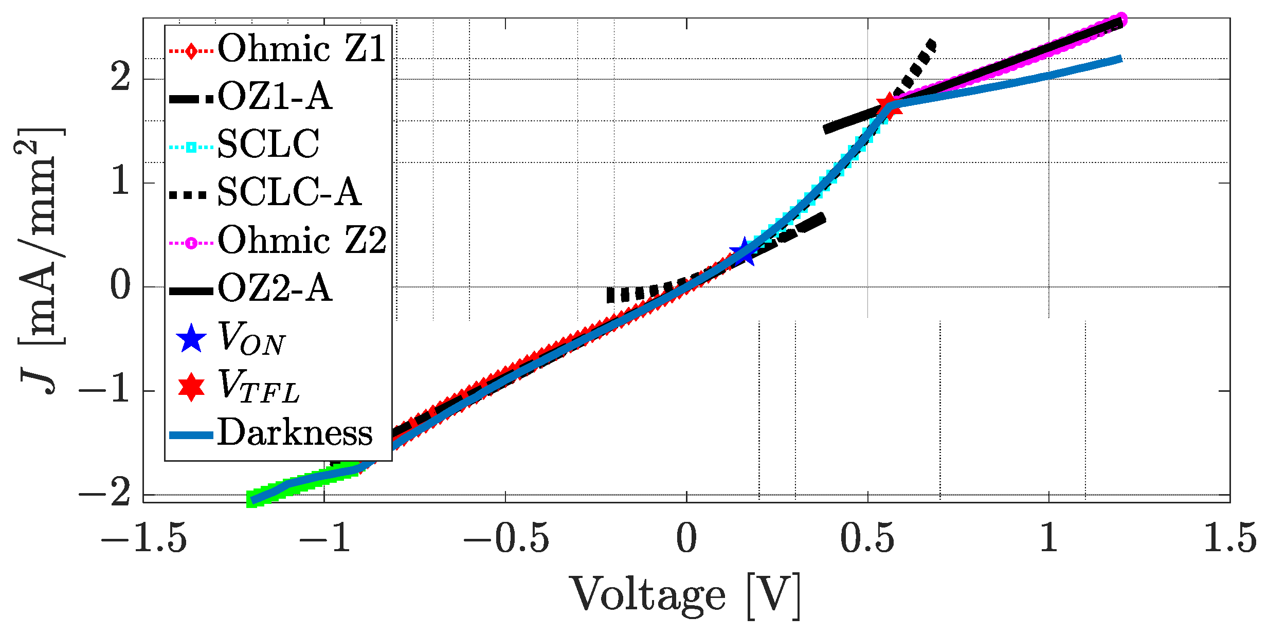
4.4. Fabrication and Electrical Characterization of the Device

In order to evaluate the electrical behavior in the (Alq3-TCNQ):Ppy film, Figure 8 shows the I-V curves for the FTO/(Alq3-TCNQ):Ppy/Ag device under the different types of used light. In Figure 8a, it can be seen that the behavior of the current is similar for all types of used light. In a visual fashion, an ohmic regime is appreciated from −1.2 V to −1 V, while the interval −1 V to 0 V shows another ohmic regime. An SCLC regime can be found from 0 V to 0.6 V, and, after 0.6 V, another ohmic regime is appreciated. Considering a cross-section area of 5.77   mm 2 , the current density–voltage (J-V) curves of the film are shown in Figure 8b; the same regimes can be seen in Figure 8a. As observed in Figure 8a,b, both the current and the current density are less in the dark condition, which means that it exhibits a photoconductive effect, and its conductivity increased due to the applied light. Since the continuous functions that describe the current densities of the device are unknown, it is not possible to determine the exact values of voltage where the regime transitions occur. The cubic spline method [76] has been applied to each J-V curve to approximate a tendency to the data from Figure 8b to fit cubic polynomials to the current density data. From cubic polynomials, it is easy to determine inflection points where changes in the concavity of the function take place and, therefore, in the current density. At some of these points, the ohmic to SCLC transition voltage V ON and the trap-filled-limit voltage V TFL are determined.
The cubic polynomials are defined by S J V = J i V = a 3 i V 3 + a 2 i V 2 + a 1 i V + a 0 i with i = 0 , , k 1 . Notice that the spline function is defined as S J V : a , b , where a = V 0 V 1 V k 1 V k = b and V = V 0 , V 1 , , V k is the data vector; furthermore, each polynomial J i V is defined as J i V : V i , V i + 1 . Moreover, a V i point is an inflection point if S J V i = 0 and S J V i > 0 . Applying the cubic spline approach and the conditions for determining inflection points, 491 inflection points were found; the histogram of the voltage values where an inflection point is localized is shown in Figure 9.
From Figure 9, the quartiles were set at 13, 56 and 70 percent of the data because the most significant concavity changes are presented in those datasets. Then, the voltage values where the most significant inflection points of the J-V curve were found are 0.88 V, 0.16 V and 0.54 V. Therefore, the voltage intervals that define the different behaviors of the J-V curve are I 1 1.2 , 0.9 , I 2 0.9 ,   0.16 and I 3 0.16 ,   0.56 . Based on these intervals, V ON = 0.16   V and V TFL = 0.56   V. The approximation curves of the ohmic and SCLC regimes as well as the transition voltages are shown in Figure 10. From Figure 10, the red curve represents the ohmic regime, which was estimated by a straight line; a cyan curve is the quadratic SCLC regime, and it can be seen that V ON joins both these regimes. On the other hand, V TFL delimits the end of the quadratic SCLC regime. Since after the V TFL an ohmic regime was observed (magenta curve), it was also approximated by a straight line.
Figure 10 also shows the J-V curve of the device under dark conditions (blue curve). The behavior of the J-V curves on the intervals can be observed. I 1 , I 2 and I 3 are similar when exposed to dark conditions and to different types of light. On the other hand, it can be seen that the slopes of the second ohmic zone, after the V TFL voltage, are different. When the applied voltage is greater than V TFL = 0.56 V in the dark condition, the current density flow is lower than that of the light condition. Conversely, the current density flow increases when the applied voltage is greater than V TFL = 0.56   V and the device is exposed to UV-Vis light. This means that the device conducts better when exposed to light. With the approximation of the ohmic to SCLC transition voltage V ON and the trap-filled-limit voltage V TFL and Equations (3) and (4), the free carrier density n 0 and the trap density N t can be determined as follows.
n 0 = 9 V ON ε 0 ε r 8 q d s 2
N t = 2 V TFL ε r q d s 2
Since V ON = 0.16 V, V TFL = 0.56 V, q = 1.6 × 10 19 C , ε 0 = 8.85418 × 10 12 C Vm   d s = 8.5 × 10 7 m and assuming a dimensionless dielectric constant ε r = 3.234 , an approximation of the free carrier density and trap density for the device are n 0 = 4.4586 × 10 19 1 m 3 and N t = 3.1333 × 10 31 1 m 3 , respectively.

5. Conclusions

In recent years, optimizing the organic semiconductor manufacturing process has been a topic of scientific interest. In these optimization processes, new organic semiconductors are used, and then it is necessary to have methodologies that allow to quickly obtain the electrical characteristics of these materials to determine if the device will have the best performance. In this sense, the hybrid film (Alq3-TCNQ):Ppy was fabricated by initially doping the hydroxyquinoline with the TCNQ and subsequently embedding the semiconductor in the polypyrrole polymer matrix. DFT calculations carried out on designed complexes of these species show that the nature of these complexes is determined by the formation of hydrogen bonds, which involve two possible cases: (i) the interaction among nitrogen terminal atoms of TCNQ moiety with peripheral hydrogen atoms from the Ppy and (ii) face to face interactions between TCNQ central hydrogen atoms and the heteroatoms from the organic rings of Ppy. The formation of these complexes rules the decrease in the HOMO-LUMO gap, as shown by the calculations. The experimental IR spectra indicate that the hybrid film did not suffer degradation during its deposit. The SEM and AFM images have confirmed that the film shows a heterogeneous morphology integrated by segregation of the Alq3-TCNQ semiconductor in the matrix, and the X-ray diffraction results confirmed that the clusters assembled in the film and that the film itself exhibits an amorphous structure. The UV-Vis spectrum of the (Alq3-TCNQ):Ppy film showed a characteristic band at 375 nm, attributed to the electron transition from the HOMO orbital in hydroxyquinoline to the LUMO orbital in the TCNQ. The optical properties of the (Alq3-TCNQ):Ppy film showed two indirect allowed transitions, with onset and optical gaps of 3.44 and 2.64 eV. Moreover, the photoluminescence measurements showed an intense visible emission in the visible region. By applying the cubic spline method to the J-V curves of the device, it was determined that the ohmic to SCLC transition voltage is V ON = 0.16 V and the trap-filled-limit voltage is V TFL = 0.56 V; then, considering that the dielectric constant is ε r = 3.234 , the free carrier density and trap density of the device were calculated, yielding n 0 = 4.4586 × 10 19 1 m 3 and N t = 3.1333 × 10 31 1 m 3 , respectively. Future work includes the determination of the charge carrier mobility of the device. From the J-V curves of the device, it was possible to verify that the current density is higher when the device is exposed to UV light, meaning the resistance to current flow decreased and, consequently, its conductivity increased. On the other hand, under dark conditions, the current density was lower, which means the device exhibits greater resistance to the passage of current, and therefore its conductivity decreased. The shape of the J-V curves demonstrates that the device has a photoconductive effect. These results indicate that the (Alq3-TCNQ):Ppy film can be used as a photoconductor in optoelectronic applications.

Author Contributions

Conceptualization, M.E.S.V. and R.S.; methodology, M.E.S.V., L.A.C.C., R.S., O.L.F., A.D. and C.R.; software, M.E.S.V., L.A.C.C. and R.S.; validation, M.E.S.V., L.A.C.C., R.S., O.L.F., A.D. and C.R.; formal analysis, M.E.S.V., C.R., A.D. and R.S.; investigation, L.A.C.C. and C.R.; resources, M.E.S.V. and R.S.; data curation, M.E.S.V., L.A.C.C., R.S., O.L.F., A.D. and C.R.; writing—original draft preparation, M.E.S.V., L.A.C.C., R.S. and C.R.; writing—review and editing, M.E.S.V., L.A.C.C., R.S., O.L.F., A.D. and C.R.; visualization, L.A.C.C. and C.R.; supervision, M.E.S.V. and R.S.; project administration, M.E.S.V.; funding acquisition, M.E.S.V. and R.S. All authors have read and agreed to the published version of the manuscript.

Funding

This research was funded by Anahuac México University, project number NNAIASEVM16070616. María Elena Sánchez Vergara gratefully acknowledges financial support from Consejo Mexiquense de Ciencia y Tecnología, Financiamiento para investigación de mujeres científicas: EDOMÉX-FICDTEM-2022-01, Project 64.

Institutional Review Board Statement

Not applicable.

Data Availability Statement

Data are contained within the article.

Acknowledgments

The authors are grateful for the technical support of Carlos Flores Morales, Fernando Gibran Mendoza López, Valeria López Valenzuela and Jimena Sánchez. Also, we want to thank Cain González, María Teresa Vázquez, Celic Martínez, Alejandro Pompa, Carlos Ramos and Oralia Jiménez for technical help.

Conflicts of Interest

The authors declare no conflict of interest.

References

  1. Newman, C.R.; Frisbie, C.D.; da Silva Filho, D.A.; Brédas, J.-L.; Ewbank, P.C.; Mann, K.R. Introduction to organic thin film transistors and design of n-channel organic semiconductors. Chem. Mater. 2004, 16, 4436–4451. [Google Scholar] [CrossRef]
  2. Dou, L.; Liu, Y.; Hong, Z.; Li, G.; Yang, Y. Low-bandgap near-IR conjugated polymers/molecules for organic electronics. Chem. Rev. 2015, 115, 12633–12665. [Google Scholar] [CrossRef] [PubMed]
  3. Murphy, A.R.; Frechet, J.M. Organic semiconducting oligomers for use in thin film transistors. Chem. Rev. 2007, 107, 1066–1096. [Google Scholar] [CrossRef] [PubMed]
  4. Sun, Q.; Dong, G.; Wang, L.; Qiu, Y. Organic optocouplers. Sci. China Chem. 2011, 54, 1017–1026. [Google Scholar] [CrossRef]
  5. Baeg, K.-J.; Binda, M.; Natali, D.; Caironi, M.; Noh, Y.-Y. Organic Light Detectors: Photodiodes and Phototransistors. Adv. Mater. 2013, 25, 4267–4295. [Google Scholar] [CrossRef] [PubMed]
  6. Seeds, A.J.; De Salles, A.A.A. Optical control of microwave semiconductor devices. IEEE Trans. Microw. Theory Tech. 1990, 38, 577–585. [Google Scholar] [CrossRef]
  7. Ross, D.A. Solid State Photodetectors—The Photoconductor. In Optoelectronic Devices and Optical Imaging Techniques; Palgrave: London, UK, 1979. [Google Scholar] [CrossRef]
  8. Piradi, V.; Yan, F.; Zhu, X.; Wong, W.-Y. A recent overview of porphyrin-based π-extended small molecules as donors and acceptors for high-performance organic solar cells. Mater. Chem. Front. 2021, 5, 7119–7133. [Google Scholar] [CrossRef]
  9. Henson, Z.B.; Müllen, K.; Bazan, G.C. Design strategies for organic semiconductors beyond the molecular formula. Nat. Chem. 2012, 4, 699–704. [Google Scholar] [CrossRef]
  10. Sun, Y.; Welch, G.C.; Leong, W.L.; Takacs, C.J.; Bazan, G.C.; Heeger, A.J. Solution-processed small-molecule solar cells with 6.7% efficiency. Nat. Mater. 2012, 11, 44–48. [Google Scholar] [CrossRef]
  11. Qin, Y.; Li, G.; Qi, T.; Huang, H. Aromatic imide/amide-based organic small-molecule emitters for organic light-emitting diodes. Mater. Chem. Front. 2020, 4, 1554–1568. [Google Scholar] [CrossRef]
  12. Yu, T.; Liu, L.; Xie, Z.; Ma, Y. Progress in small-molecule luminescent materials for organic light-emitting diodes. Sci. China Chem. 2015, 58, 907–915. [Google Scholar] [CrossRef]
  13. Venkateswararao, A.; Wong, K.-T. Small molecules for vacuum-processed organic photovoltaics: Past, current status, and prospect. Bull. Chem. Soc. Jpn. 2021, 94, 812–838. [Google Scholar] [CrossRef]
  14. Hains, A.W.; Liang, Z.; Woodhouse, M.A.; Gregg, B.A. Molecular semiconductors in organic photovoltaic cells. Chem. Rev. 2010, 110, 6689–6735. [Google Scholar] [CrossRef] [PubMed]
  15. Yamao, T.; Miki, T.; Akagami, H.; Nishimoto, Y.; Ota, S.; Hotta, S. Direct formation of thin single crystals of organic semiconductors onto a substrate. Chem. Mater. 2007, 19, 3748–3753. [Google Scholar] [CrossRef]
  16. Placencia, D.; Wang, W.; Shallcross, R.C.; Nebesny, K.W.; Brumbach, M.; Armstrong, N.R. Organic photovoltaic cells based on solvent-annealed, textured titanyl phthalocyanine/C60 heterojunctions. Adv. Funct. Mater. 2009, 19, 1913–1921. [Google Scholar] [CrossRef]
  17. Gregg, B.A.; Sprague, J.; Peterson, M.W. Long-range singlet energy transfer in perylene bis (phenethylimide) films. J. Phys. Chem. B 1997, 101, 5362–5369. [Google Scholar] [CrossRef]
  18. Babu, B.H.; Lyu, C.; Yu, C.; Wen, Z.; Li, F.; Hao, X.-T. Role of Central Metal Ions in 8-Hydroxyquinoline-Doped ZnO Interfacial Layers for Improving the Performance of Polymer Solar Cells. Adv. Mater. Interfaces 2018, 5, 1801172. [Google Scholar] [CrossRef]
  19. Onlaor, K.; Tunhoo, B.; Thiwawong, T.; Nukeaw, J. Electrical bistability of tris-(8-hydroxyquinoline) aluminum (Alq3)/ZnSe organic-inorganic bistable device. Curr. Appl. Phys. 2012, 12, 331–336. [Google Scholar] [CrossRef]
  20. Shahedi, Z.; Jafari, M.R.; Zolanvari, A.A. Synthesis of ZnQ2, CaQ2, and CdQ2 for application in OLED: Optical, thermal, and electrical characterizations. J. Mater. Sci. Mater. Electron. 2017, 28, 7313–7319. [Google Scholar] [CrossRef]
  21. Keshmiri, L.; Elahi, S.M.; Jafari, M.R.; Jafari, F.; Parhizgar, S.S. The blue-shift of photoluminescence spectra of zinc complexes of 8-hydroxyquinoline by addition of ZnO nanoparticles. J. Electron. Mater. 2018, 47, 1526–1532. [Google Scholar] [CrossRef]
  22. Haggag, S.M.; Farag, A.A.; Abdelrafea, M. Spectral, thermal and optical–electrical properties of the layer-by-layer deposited thin film of nano Zn(II)-8-hydroxy-5-nitrosoquinolate complex. Spectrochim. Acta A Mol. Biomol. Spectrosc. 2013, 110, 14–19. [Google Scholar] [CrossRef] [PubMed]
  23. Painuly, D.; Masram, D.T.; Rabanal, M.E.; Nagpure, I.M. The effect of ethanol on structural, morphological and optical properties of Li(I) 8–hydroxyquinoline phosphor. J. Lumin. 2017, 192, 1180–1190. [Google Scholar] [CrossRef]
  24. Sevgili, O.; Canlı, S.; Akman, F.; Orak, I.; Karabulut, A.; Yıldırım, N. Characterization of aluminum 8-hydroxyquinoline microbelts and microdots, and photodiode applications. J. Phys. Chem. Solids 2020, 136, 109128. [Google Scholar] [CrossRef]
  25. Demir, R.; Kaya, İ. Comparison of electrical characteristics of zinc oxide and cadmium sulfide films covered with 8-hydroxyquinoline for diode applications. J. Mater. Sci. Mater. Electron. 2019, 30, 7103–7109. [Google Scholar] [CrossRef]
  26. El-Nahass, M.M.; Farid, A.M.; Atta, A.A. Structural and optical properties of Tris(8-hydroxyquinoline) aluminum (III)(Alq3) thermal evaporated thin films. J. Alloys Compd. 2010, 507, 112–119. [Google Scholar] [CrossRef]
  27. Dai, C.; Shang, F.; Wei, Z.; Chen, Z.; Yan, X.; Ji, Z.; Pang, Z.; Han, S. Room temperature ferromagnetic and optical properties of rare earth Sm-doped tris(8-hydroxyquinoline) gallium thin films. Thin Solid Films 2018, 648, 113–119. [Google Scholar] [CrossRef]
  28. Bakhshipour, S.; Shahedi, Z.; Mirahmadi, F.; Fereidonnejad, R.; Hesani, M. Effect of different in situ temperatures on the crystallinity and optical properties of green synthesized 8-hydroxyquinoline zinc by saffron extract. Opt. Contin. 2022, 1, 1401–1412. [Google Scholar] [CrossRef]
  29. Dumur, F. Zinc complexes in OLEDs: An overview. Synth. Met. 2014, 195, 241–251. [Google Scholar] [CrossRef]
  30. Shahedi, Z.; Zare, H.; Sediqy, A. Manufacturing of nanoflowers crystal of ZnQ2 by a co-precipitation process and their morphology-dependent luminescence properties. J. Mater. Sci. Mater. Electron 2021, 32, 6843–6854. [Google Scholar] [CrossRef]
  31. Requena, F.; Crespo, M. Recent advances on phosphorescent cycloplatinated compounds containing tetradentate nitrogen ligands for OLED applications. Inorg. Chem. Res. 2022, 6, 39–47. [Google Scholar]
  32. Jiang, F.; Song, J.; Dong, M.; Wang, Y. Preparation and Characterization of Paramagnetic Bis (8-Hydroxyquinoline) Manganese Crystals. Materials 2020, 13, 2379. [Google Scholar] [CrossRef]
  33. Ghedini, M.; La Deda, M.; Aiello, I.; Grisolia, A. Synthesis and photophysical characterisation of soluble photoluminescent metal complexes with substituted 8-hydroxyquinolines. Synth. Met. 2003, 138, 189–192. [Google Scholar] [CrossRef]
  34. Mohana, J.; Ahila, G.; Bharathi, M.D.; Anbalagan, G. Growth, spectral, optical, thermal, and mechanical behaviour of an organic single crystal: Quinolinium 2-carboxy 6-nitrophthalate monohydrate. J. Cryst. Growth 2016, 450, 181–189. [Google Scholar] [CrossRef]
  35. Saeed, A.; Razvi, M.A.; Salah, N. Third-order nonlinear optical properties of the small-molecular organic semiconductor tris (8-Hydroxyquinoline) aluminum by CW Z-scan technique. Results Phys. 2021, 24, 104162. [Google Scholar] [CrossRef]
  36. Katakura, R.; Koide, Y. Configuration-specific synthesis of the facial and meridional isomers of tris(8-hydroxyquinolinate)aluminum (Alq3). Inorg. Chem. 2006, 45, 5730–5732. [Google Scholar] [CrossRef]
  37. Rajeswaran, M.; Blanton, T.N.; Young, R.H.; Brennessel, W. Modeling Disorder in the Crystal Structure of the α Polymorph of Alq3. J. Chem. Crystallogr. 2010, 40, 195–200. [Google Scholar] [CrossRef]
  38. Kaji, H.; Kusaka, Y.; Onoyama, G.; Horii, F. Relationships between light-emitting properties and different isomers in polymorphs of tris(8-hydroxyquinoline) aluminum (III)(Alq3) analyzed by solid-state 27Al NMR and density functional theory (DFT) calculations. Jpn. J. App. Phys. 2005, 44, 3706. [Google Scholar] [CrossRef]
  39. Saeed, A.; Al-Buriahi, M.S.; Razvi, M.A.; Salah, N.; Al-Hazmi, F.E. Electrical and dielectric properties of meridional and facial Alq3 nanorods powders. J. Mater. Sci. Mater. Electron 2021, 32, 2075–2087. [Google Scholar] [CrossRef]
  40. McElvain, J.; Antoniadis, H.; Hueschen, M.R.; Miller, J.N.; Roitman, D.M.; Sheats, J.R.; Moon, R.L. Formation and growth of black spots in organic light-emitting diodes. J. Appl. Phys. 1996, 80, 6002–6007. [Google Scholar] [CrossRef]
  41. Do, L.-M.; Oyamada, M.; Koike, A.; Han, E.-M.; Yamamoto, N.; Fujihira, M. Morphological change in the degradation of Al electrode surfaces of electroluminescent devices by fluorescence microscopy and AFM. Thin Solid Films 1996, 273, 209–213. [Google Scholar] [CrossRef]
  42. Tang, C.W.; VanSlyke, S.A. Organic electroluminescent diodes. Appl. Phys. Lett. 1987, 51, 913–915. [Google Scholar] [CrossRef]
  43. Lam, T.-N.; Huang, Y.-L.; Weng, K.-C.; Lai, Y.-L.; Lin, M.-W.; Chu, Y.-H.; Lin, H.-J.; Kaun, C.-C.; Wei, D.-H.; Tseng, Y.-C.; et al. Spin filtering of a termination-controlled LSMO/Alq3 heterojunction for an organic spin valve. J. Mater. Chem. C 2017, 5, 9128–9137. [Google Scholar] [CrossRef]
  44. Kao, P.-C.; Chu, S.-Y.; Huang, H.-H.; Tseng, Z.-L.; Chen, Y.-C. Improved efficiency of organic photovoltaic cells using tris (8-hydroxy-quinoline) aluminum as a doping material. Thin Solid Films 2009, 517, 5301–5304. [Google Scholar] [CrossRef]
  45. Varo, P.L.; Tejada, J.J.; Villanueva, J.L.; Carceller, J.E.; Deen, M.J. Modeling the transition from ohmic to space charge limited current in organic semiconductors. Org. Electron. 2012, 13, 1700–1709. [Google Scholar] [CrossRef]
  46. Abdel-Malik, T.G.; Cox, G.A. Charge transport in nickel phthalocyanine crystals. I. Ohmic and space-charge-limited currents in vacuum ambient. J. Phys. C Solid State Phys. 1977, 10, 63. [Google Scholar] [CrossRef]
  47. Moiz, S.A.; Ahmed, M.M.; Karimov, K.S. Estimation of Electrical Parameters of OD Organic Semiconductor Diode from Measured I-V Characteristics. ETRI J. 2005, 27, 319–325. [Google Scholar] [CrossRef]
  48. Kim, K.M.; Choi, B.J.; Lee, M.H.; Kim, G.H.; Song, S.J.; Seok, J.Y.; Hwang, C.S. A detailed understanding of the electronic bipolar resistance switching behavior in Pt/TiO2/Pt structure. Nanotechnology 2011, 22, 254010. [Google Scholar] [CrossRef]
  49. Kim, K.M.; Choi, B.J.; Shin, Y.C.; Choi, S.; Hwang, C.S. Anode-interface localized filamentary mechanism in resistive switching of TiO2 thin films. App. Phys. Lett. 2007, 91, 012907. [Google Scholar] [CrossRef]
  50. Mott, N.F.; Gurney, R.W. Electronic Processes in Ionic Crystals, 2nd ed.; Dover Publications: Oxford, UK, 1946. [Google Scholar]
  51. Gucciardi, P.G.; Trusso, S.; Vasi, C.; Patane, S.; Allegrini, M. Nano-Raman imaging of Cu–TCNQ clusters in TCNQ thin films by scanning near-field optical microscopy. Phys. Chem. Chem. Phys. 2002, 4, 2747–2753. [Google Scholar] [CrossRef]
  52. Bendikov, M.; Wudl, F.; Perepichka, D.F. Tetrathiafulvalenes, oligoacenenes, and their buckminsterfullerene derivatives: The brick and mortar of organic electronics. Chem. Rev. 2004, 104, 4891–4946. [Google Scholar] [CrossRef]
  53. Roncali, J. Molecular engineering of the band gap of π-conjugated systems: Facing technological applications. Macromol. Rapid Commun. 2007, 28, 1761–1775. [Google Scholar] [CrossRef]
  54. Frisch, M.J.; Trucks, G.W.; Schlegel, H.B.; Scuseria, G.E.; Robb, M.; Cheeseman, J.R.; Scalmani, G.; Barone VP, G.A.; Petersson, G.A.; Nakatsuji, H.J.R.A. Gaussian 16, Revision A. 03; Gaussian Inc.: Wallingford, CT, USA, 2016. [Google Scholar]
  55. Becke, A.D. Density-functional exchange-energy approximation with correct asymptotic behavior. Phys. Rev. A 1988, 38, 3098. [Google Scholar] [CrossRef] [PubMed]
  56. Perdew, J.P.; Wang, Y. Accurate and simple analytic representation of the electron-gas correlation energy. Phys. Rev. B 1992, 45, 13244. [Google Scholar] [CrossRef] [PubMed]
  57. Min, D.; Cho, M.; Khan, A.R.; Li, S. Charge transport properties of dielectrics revealed by isothermal surface potential decay. IEEE Trans. Dielectr. Electr. Insul. 2012, 19, 1465–1473. [Google Scholar] [CrossRef]
  58. Varo, P.L.; Tejada, J.J.; Villanueva, J.L.; Deen, M.J. Space-charge and injection limited current in organic diodes: A unified model. Org. Electron. 2014, 15, 2526–2535. [Google Scholar] [CrossRef]
  59. Bhutta, M.S.; Akram, S.; Meng, P.; Castellon, J.; Agnel, S.; Li, H.; Guo, Y.; Rasool, G.; Hussain, S.; Nazir, M.T. Steady-state conduction current performance for multilayer polyimide/SiO2 films. Polymers 2021, 13, 640. [Google Scholar] [CrossRef]
  60. Zhu, G.-Z.; Wang, L.-S. Communication: Vibrationally resolved photoelectron spectroscopy of the tetracyanoquinodimethane (TCNQ) anion and accurate determination of the electron affinity of TCNQ. J. Chem. Phys. 2015, 143, 221102. [Google Scholar] [CrossRef] [PubMed]
  61. Scharber, M.C.; Sariciftci, N.S. Low band gap conjugated semiconducting polymers. Adv. Mater. Technol. 2021, 6, 2000857. [Google Scholar] [CrossRef]
  62. Havinga, E.E.; Ten Hoeve, W.; Wynberg, H.J. A new class of small band gap organic polymer conductors. Polym. Bull. 1992, 29, 119–126. [Google Scholar] [CrossRef]
  63. Phillips, J.P.; Deye, J.F. Infrared spectra of oxine chelates. Anal. Chim. Acta 1957, 17, 231–233. [Google Scholar] [CrossRef]
  64. Gavrilko, T.; Fedorovich, R.; Dovbeshko, G.; Marchenko, A.; Naumovets, A.; Nechytaylo, V.; Puchkovska, G.; Viduta, L.; Baran, J. Ratajczak HFTIR spectroscopic STM studies of vacuum deposited aluminium (III) 8-hydroxyquinoline thin films. J. Mol. Struct. 2004, 704, 163–168. [Google Scholar] [CrossRef]
  65. Tackett, J.E.; Sawyer, D.T. Properties and infrared spectra in the potassium bromide region of 8-quinolinol and its metal chelates. Inorg. Chem. 1964, 3, 692–696. [Google Scholar] [CrossRef]
  66. Engelter, C.; Jackson, G.E.; Knight, C.L.; Thornton, D.A. Spectra-structure correlations from the infrared spectra of some transition metal complexes of 8-hydroxyquinoline. J. Mol. Struct. 1989, 213, 133–144. [Google Scholar] [CrossRef]
  67. Bredas, J.L.; Silbey, R.; Boudreaux, D.S.; Chance, R.R. Chain-length dependence of electronic and electrochemical properties of conjugated systems: Polyacetylene, polyphenylene, polythiophene, and polypyrrole. J. Am. Chem. Soc. 1983, 105, 6555–6559. [Google Scholar] [CrossRef]
  68. Tauc, J. Optical properties and electronic structure of amorphous Ge and Si. Mater. Res. Bull. 1968, 3, 37–46. [Google Scholar] [CrossRef]
  69. Urbach, F. The long-wavelength edge of photographic sensitivity and of the electronic absorption of solids. Phys. Rev. 1953, 92, 1324. [Google Scholar] [CrossRef]
  70. Alosabi, A.Q.; Al-Muntaser, A.A.; El-Nahass, M.M.; Oraby, A.H. Structural, optical and DFT studies of disodium phthalocyanine thin films for optoelectronic devices applications. Opt. Laser Technol. 2022, 155, 108372. [Google Scholar] [CrossRef]
  71. Dongol, M.; El-Nahass, M.M.; El-Denglawey, A.; Elhady, A.F.; Abuelwafa, A.A. Optical properties of nano 5, 10, 15, 20-tetraphenyl-21H,23H-prophyrin nickel (II) thin films. Curr. Appl. Phys. 2012, 12, 1178–1184. [Google Scholar] [CrossRef]
  72. Hill, I.G.; Kahn, A.; Soos, Z.G.; Pascal, R.A., Jr. Charge-separation energy in films of π-conjugated organic molecules. Chem. Phys. Lett. 2000, 327, 181–188. [Google Scholar] [CrossRef]
  73. Hamdalla, T.; Darwish, A.A.A.; Al-Ghamdi, S.A.; Alzahrani, A.O.M.; El-Zaidia, E.F.M.; Alamrani, N.A.; Elblbesy, M.A.; Yahia, I.S. Preparation, Raman spectroscopy, surface morphology and optical properties of TiPcCl2 nanostructured films: Thickness effect. Opt. Quantum Electron. 2021, 53, 514. [Google Scholar] [CrossRef]
  74. Ghanem, M.G.; Badr, Y.; Hameed, T.A.; El Marssi, M.; Lahmar, A.; Wahab, H.A.; Battisha, I.K. Synthesis and characterization of undoped and Er-doped ZnO nano-structure thin films deposited by sol-gel spin coating technique. Mater. Res. Express 2019, 6, 085916. [Google Scholar] [CrossRef]
  75. Farruggia, G.; Iotti, S.; Prodi, L.; Montalti, M.; Zaccheroni, N.; Savage, P.B.; Trapani, V.; Sale, P. Wolf FI 8-Hydroxyquinoline Derivatives as Fluorescent Sensors for Magnesium in Living Cells. J. Am. Chem. Soc. 2006, 128, 344–350. [Google Scholar] [CrossRef]
  76. De Boor, C. A Practical Guide to Splines; Springer: New York, NY, USA, 1978. [Google Scholar]
Figure 1. (a) Diagram of the photoconductor device for electrical characterization. (b) Current density-voltage characteristic [59].
Sensors 23 07708 g001
Figure 2. Optimized structures of (a) Hal-TCNQ1 and (b) Hal-TCNQ2. (Code color: carbon, grey; oxygen, red; nitrogen, blue and pink aluminium).
Sensors 23 07708 g002
Figure 3. Frontier molecular orbitals for hAl-TCNQ1: (a) HOMO, (b) LUMO and hAl-TCNQ2, (c) HOMO and (d) LUMO. (The green and red colors represent the positive and negative phases of the molecular orbitals respectively).
Sensors 23 07708 g003
Figure 4. Calculated IR spectrum for (a) hAl-TCNQ1, (b) hAl-TCNQ2 and (c) experimental IR spectrum for Alq3-TCNQ in KBr pellet.
Sensors 23 07708 g004
Figure 5. (a) SEM, (b) DRX pattern and (c) AFM measurements of the (Alq3-TCNQ):Ppy film.
Sensors 23 07708 g005
Figure 6. (a) Absorbance spectra, (b) % transmittance, (c) Tauc plot and (d) variation in ln(α) with hν for (Alq3-TCNQ):Ppy film. The slope for the Urbach energy was calculated on the red line.
Sensors 23 07708 g006
Figure 7. Photoluminescence spectra of the (Alq3-TCNQ):Ppy film at room temperature with a UV laser.
Sensors 23 07708 g007
Figure 8. (a) Current–voltage curves and (b) current density–voltage curves of FTO/(Alq3-TCNQ):Ppy/Ag device.
Sensors 23 07708 g008
Figure 9. Inflection points histogram.
Sensors 23 07708 g009
Figure 10. Approximation of the J-V graphs.
Sensors 23 07708 g010
Table 1. Distance and Wiberg index of the interacting atoms in hAl-TCNQ1 and hAl-TCNQ2.
Distance (Å)Wiberg Index
Alq3TCNQhAl-TCNQ1
N (62)N (53)
H (22) 2.85 0.0018
H (23) 2.76 0.0024
H (49)2.49 0.0074
Alq3TCNQhAl-TCNQ2
N (53)H (69)H (70)
H (15)2.69 0.0036
O (32) 3.04 0.0023
O (51) 2.0790.0257
Table 2. Calculated and experimental IR frequencies and their assignment for Alq3-TCNQ.
hAl-TCNQ1
ν (cm−1)
Simulated
hAl-TCNQ2
ν (cm−1)
Simulated
Alq3-TCNQ
ν (cm−1)
KBr Pellet
(Alq3-TCNQ):Ppy
ν (cm−1)
Film
Assignment
1630163016071609C=C
1596160715821591C=N
1450146314691466C-C
1150115811691156C-C-H
774, 655770, 659781, 646772, 648in-plane ring deformations
2291229922152217CN-stretching mode
Disclaimer/Publisher’s Note: The statements, opinions and data contained in all publications are solely those of the individual author(s) and contributor(s) and not of MDPI and/or the editor(s). MDPI and/or the editor(s) disclaim responsibility for any injury to people or property resulting from any ideas, methods, instructions or products referred to in the content.

