
Design and Test of a New Dielectric-Loaded Resonator for the Accurate Characterization of Conductive and Dielectric Materials
 , ,
, ,  , and
, and
Abstract
:1. Introduction
2. Measurement Methods
2.1. Surface Resistance Measurement Method
2.2. Complex Permittivity Measurement Method
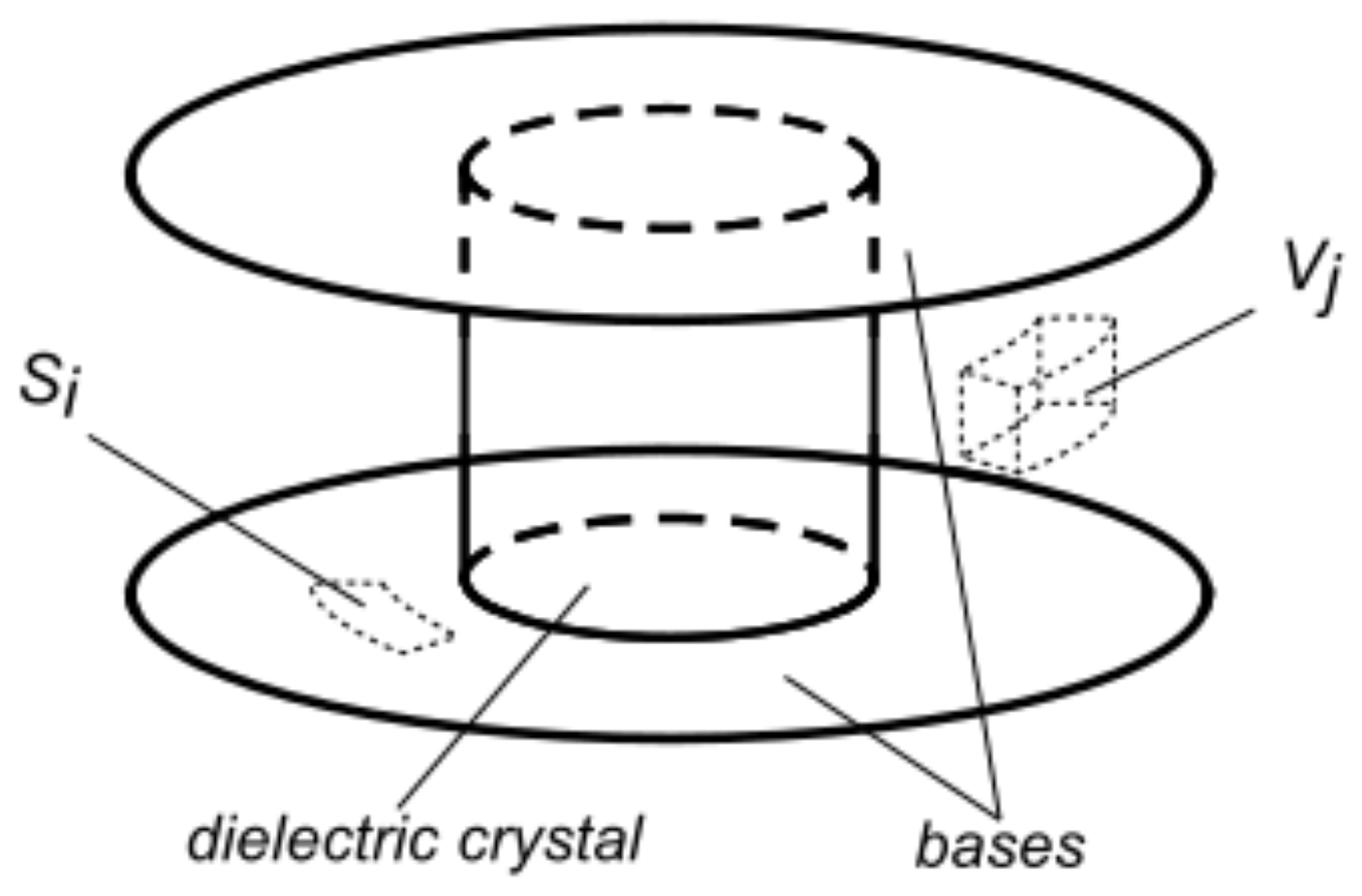
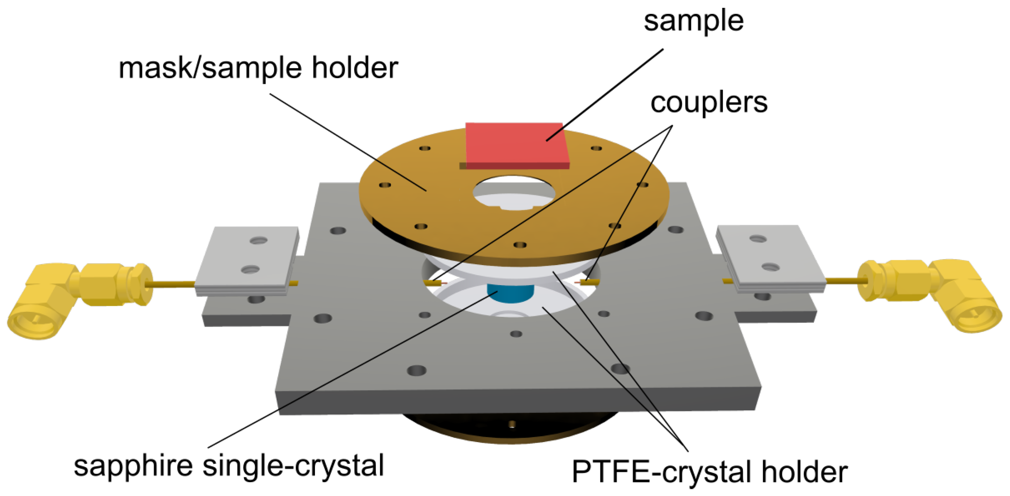
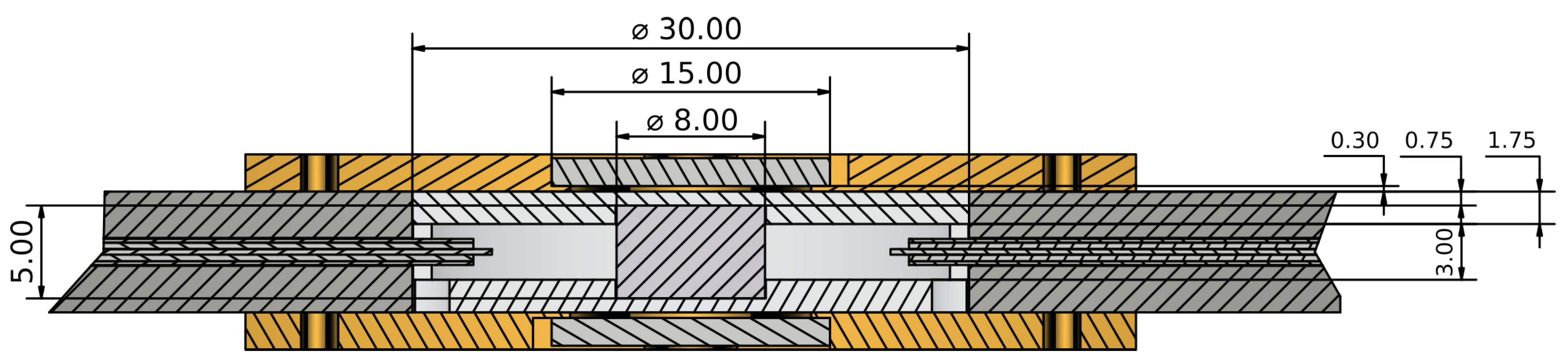
3. Design and Realization of the DR
- Improvement in the measurement repeatability: a closed configuration in which the sample can be loaded from the outside without the need of disassembling the whole DR for each measurement is preferred;
- Possibility of hosting two samples at the same time: this can be used to perform multiple-sample comparisons [41] or to increase the sensitivity when needed;
- Contactless measurements: the sample holder must be designed to support the samples without letting the probed area of the sample touch other surfaces. This is useful to avoid damaging delicate sample surfaces and/or coatings.
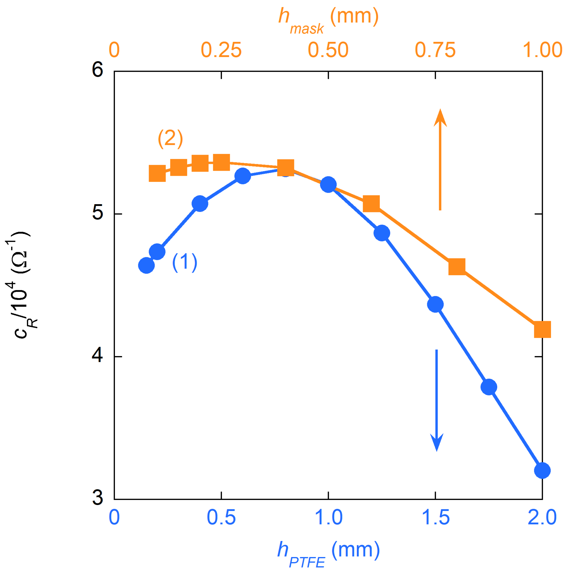
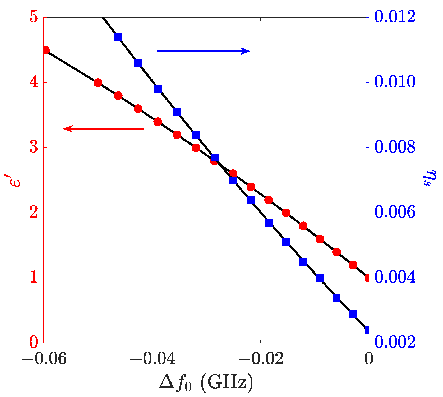
3.1. Dimensions Optimization— Measurements
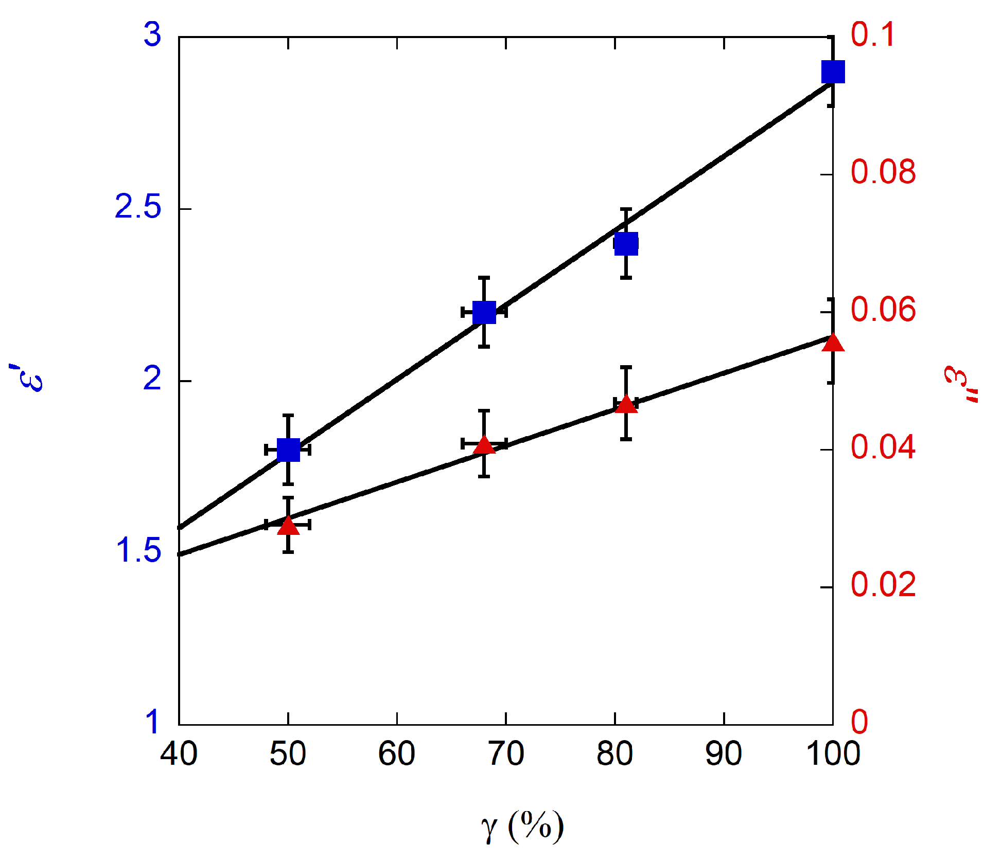
3.2. Dimensions Optimization— Measurements
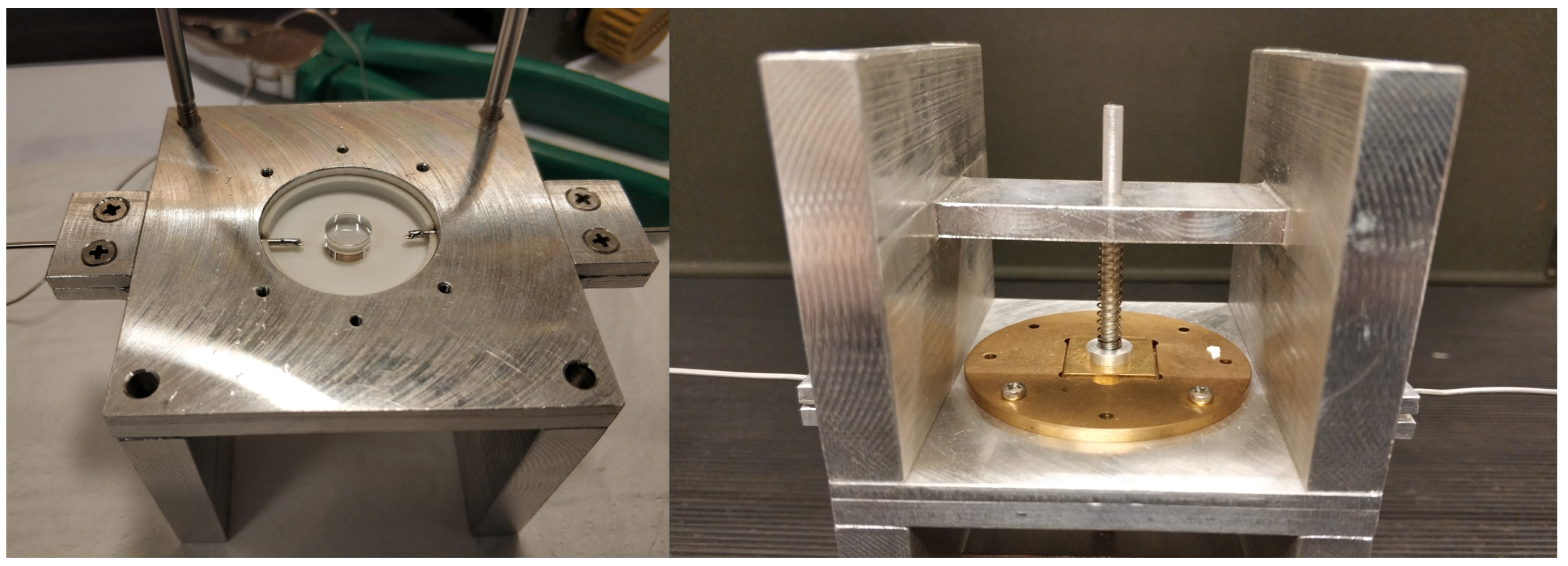
3.3. Realization of the DR
4. Experimental Tests and Performances Analysis
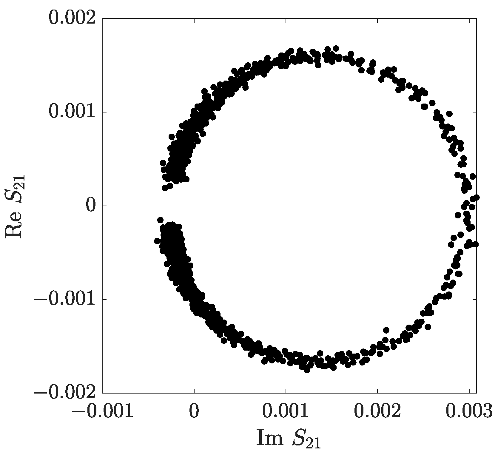
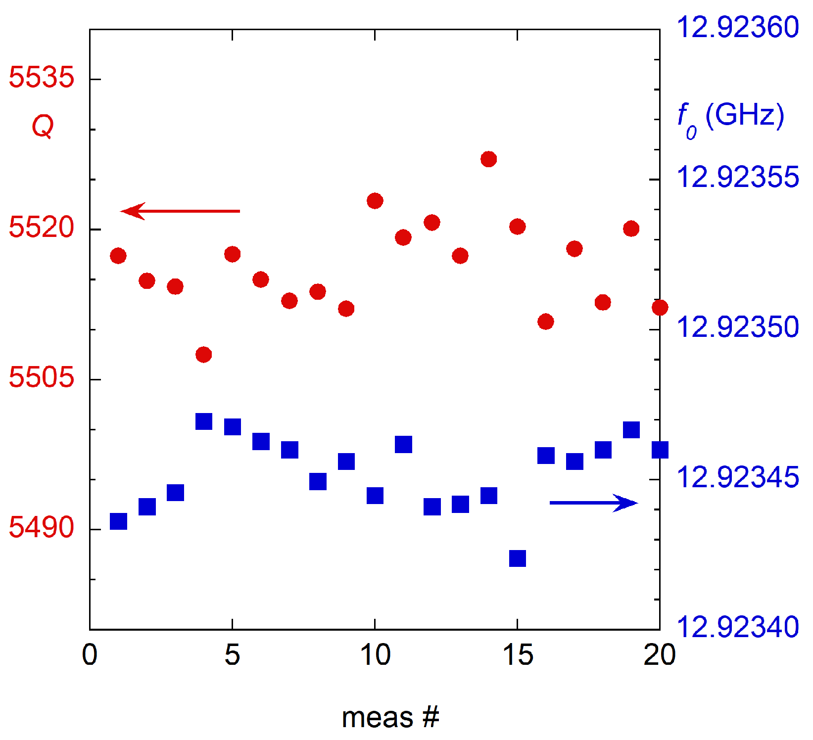
4.1. Measurement Repeatability
4.2. Measurements and Uncertainty Evaluation
4.2.1. Differential Measurement
4.2.2. Absolute Measurement
4.3. Measurements and Uncertainty Evaluation
5. Comparison with the State of the Art
6. Summary
Author Contributions
Funding
Institutional Review Board Statement
Informed Consent Statement
Data Availability Statement
Acknowledgments
Conflicts of Interest
References
- Kaatze, U. Techniques for measuring the microwave dielectric properties of materials. Metrologia 2010, 47, S91. [Google Scholar] [CrossRef]
- Chen, L.F.; Ong, C.; Neo, C.; Varadan, V.; Varadan, V.K. Microwave Electronics: Measurement and Materials Characterization; John Wiley & Sons: Hoboken, NJ, USA, 2004. [Google Scholar]
- Courtney, W.E. Analysis and evaluation of a method of measuring the complex permittivity and permeability microwave insulators. IEEE Trans. Microw. Theory Tech. 1970, 18, 476–485. [Google Scholar] [CrossRef]
- Krupka, J. Contactless methods of conductivity and sheet resistance measurement for semiconductors, conductors and superconductors. Meas. Sci. Technol. 2013, 24, 062001. [Google Scholar] [CrossRef]
- Adam, S.F. A new precision automatic microwave measurement system. IEEE Trans. Instrum. Meas. 1968, 17, 308–313. [Google Scholar] [CrossRef]
- Karbowiak, A. An instrument for the measurement of surface impedance at microwave frequencies. Proc. IEE-Part B Radio Electron. Eng. 1958, 105, 195–203. [Google Scholar] [CrossRef]
- Roussy, G.; Felden, M. A sensitive method for measuring complex permittivity with a microwave resonator. IEEE Trans. Microw. Theory Tech. 1966, 14, 171–175. [Google Scholar] [CrossRef]
- Harris, F.E.; O’Konski, C.T. Measurement of High Permittivity Dielectrics at Microwave Frequencies. Rev. Sci. Instrum. 1955, 26, 482–485. [Google Scholar] [CrossRef]
- Krupka, J. An accurate method for permittivity and loss tangent measurements of low loss dielectric using TE/sub 01 delta/dielectric resonators. In Proceedings of the 1988 Fifth International Conference on Dielectric Materials, Measurements and Applications, Canterbury, UK, 27–30 June 1988; pp. 322–325. [Google Scholar]
- Afsar, M.N.; Birch, J.R.; Clarke, R.; Chantry, G. The measurement of the properties of materials. Proc. IEEE 1986, 74, 183–199. [Google Scholar] [CrossRef]
- Leong, K.; Mazierska, J. Precise measurements of the Q factor of dielectric resonators in the transmission mode-accounting for noise, crosstalk, delay of uncalibrated lines, coupling loss, and coupling reactance. IEEE Trans. Microw. Theory Tech. 2002, 50, 2115–2127. [Google Scholar] [CrossRef]
- D’Alvia, L.; Pittella, E.; Rizzuto, E.; Piuzzi, E.; Del Prete, Z. A portable low-cost reflectometric setup for moisture measurement in cultural heritage masonry unit. Measurement 2022, 189, 110438. [Google Scholar] [CrossRef]
- Sene, B.; Reiter, D.; Knapp, H.; Pohl, N. Design of a cost-efficient monostatic radar sensor with antenna on chip and lens in package. IEEE Trans. Microw. Theory Tech. 2021, 70, 502–512. [Google Scholar] [CrossRef]
- Nassar, I.T.; Weller, T.M.; Tsang, H. 3-D printed antenna arrays for harmonic radar applications. In Proceedings of the WAMICON 2014, Tampa, FL, USA, 6 June 2014; pp. 1–4. [Google Scholar]
- Wirth, S.G.; Morrow, I.L. Near-field microwave sensor composed of 3D printed antennas and lenses. In Proceedings of the 2018 IEEE MTT-S International Conference on Numerical Electromagnetic and Multiphysics Modeling and Optimization (NEMO), Reykjavik, Iceland, 8–10 August 2018; pp. 1–4. [Google Scholar]
- Harter, M.; Hildebrandt, J.; Ziroff, A.; Zwick, T. Self-calibration of a 3-D-digital beamforming radar system for automotive applications with installation behind automotive covers. IEEE Trans. Microw. Theory Tech. 2016, 64, 2994–3000. [Google Scholar] [CrossRef]
- Zhang, B.; Zirath, H. Metallic 3-D printed rectangular waveguides for millimeter-wave applications. IEEE Trans. Compon. Packag. Manuf. Technol. 2016, 6, 796–804. [Google Scholar] [CrossRef]
- Patel, A.M.; Grbic, A. A printed leaky-wave antenna based on a sinusoidally-modulated reactance surface. IEEE Trans. Antennas Propag. 2011, 59, 2087–2096. [Google Scholar] [CrossRef]
- Castelli Gattinara Di Zubiena, F.; D’Alvia, L.; Del Prete, Z.; Palermo, E. A static characterization of stretchable 3D-printed strain sensor for restoring proprioception in amputees. In Proceedings of the 2022 IEEE International Conference on Flexible and Printable Sensors and Systems (FLEPS), Vienna, Austria, 10–13 July 2022; pp. 1–4. [Google Scholar]
- Jackson, J.D. Classical Electrodynamics; John Wiley & Sons: Hoboken, NJ, USA, 2007. [Google Scholar]
- Baker-Jarvis, J.; Geyer, R.G.; Grosvenor, J.; Janezic, M.D.; Jones, C.A.; Riddle, B.; Weil, C.M.; Krupka, J. Dielectric characterization of low-loss materials a comparison of techniques. IEEE Trans. Dielectr. Electr. Insul. 1998, 5, 571–577. [Google Scholar] [CrossRef]
- Krupka, J.; Klinger, M.; Kuhn, M.; Baryanyak, A.; Stiller, M.; Hinken, J.; Modelski, J. Surface resistance measurements of HTS films by means of sapphire dielectric resonators. IEEE Trans. Appl. Supercond. 1993, 3, 3043–3048. [Google Scholar] [CrossRef]
- Mazierska, J. Dielectric resonator as a possible standard for characterization of high temperature superconducting films for microwave applications. J. Supercond. 1997, 10, 73–84. [Google Scholar] [CrossRef]
- Romanov, A.; Krkotić, P.; Telles, G.; O’Callaghan, J.; Pont, M.; Perez, F.; Granados, X.; Calatroni, S.; Puig, T.; Gutierrez, J. High frequency response of thick REBCO coated conductors in the framework of the FCC study. Sci. Rep. 2020, 10, 1–12. [Google Scholar] [CrossRef]
- Mazierska, J.; Wilker, C. Accuracy issues in surface resistance measurements of high temperature superconductors using dielectric resonators (corrected). IEEE Trans. Appl. Supercond. 2001, 11, 4140–4147. [Google Scholar] [CrossRef]
- Lee, S.Y.; Soh, B.; Ahn, J.; Cho, J.; Park, B.; Jung, C.; Fedorov, V.; Denisov, A.; Kim, Y.; Hahn, T.; et al. Use of a dielectric-loaded cylindrical cavity in measurements of the microwave surface resistances of high-T/sub c/superconducting thin films. IEEE Trans. Appl. Supercond. 1997, 7, 2013–2017. [Google Scholar]
- Kobayashi, Y.; Kayano, H. An improved dielectric resonator method for surface impedance measurement of high-T/sub c/superconductors. In Proceedings of the 1992 IEEE MTT-S Microwave Symposium Digest, Albuquerque, NM, USA, 1–5 June 1992; pp. 1031–1034. [Google Scholar]
- Pompeo, N.; Torokhtii, K.; Alimenti, A.; Sylva, G.; Braccini, V.; Silva, E. Pinning properties of FeSeTe thin film through multifrequency measurements of the surface impedance. Supercond. Sci. Technol. 2020, 33, 114006. [Google Scholar] [CrossRef]
- Pompeo, N.; Alimenti, A.; Torokhtii, K.; Bartolomé, E.; Palau, A.; Puig, T.; Augieri, A.; Galluzzi, V.; Mancini, A.; Celentano, G.; et al. Intrinsic anisotropy and pinning anisotropy in nanostructured YBa2Cu3O7−δ from microwave measurements. Supercond. Sci. Technol. 2020, 33, 044017. [Google Scholar] [CrossRef]
- Pompeo, N.; Alimenti, A.; Torokhtii, K.; Sylva, G.; Braccini, V.; Silva, E. Microwave properties of Fe(Se,Te) thin films in a magnetic field: Pinning and flux flow. J. Phys. Conf. Ser. 2020, 1559, 012055. [Google Scholar] [CrossRef]
- Alimenti, A.; Pompeo, N.; Torokhtii, K.; Spina, T.; Flükiger, R.; Muzzi, L.; Silva, E. Microwave measurements of the high magnetic field vortex motion pinning parameters in Nb3Sn. Supercond. Sci. Technol. 2020, 34, 014003. [Google Scholar] [CrossRef]
- Pompeo, N.; Alimenti, A.; Torokhtii, K.; Silva, E. Physics of vortex motion by means of microwave surface impedance measurements. J. Low Temp. Phys. 2020, 46, 343–347. [Google Scholar] [CrossRef]
- Hagen, E.; Rubens, H. Über Beziehungen des Reflexions-und Emissionsvermögens der Metalle zu ihrem elektrischen Leitvermögen. Ann. Phys. 1903, 316, 873–901. [Google Scholar] [CrossRef] [Green Version]
- Tischer, F. Effect of surface roughness on surface resistance of plane copper surfaces at millimetre waves. In Proceedings of the Institution of Electrical Engineers; IET: London, UK, 1974; Volume 121, pp. 333–336. [Google Scholar]
- Morgan, S.P., Jr. Effect of surface roughness on eddy current losses at microwave frequencies. J. Appl. Phys. 1949, 20, 352–362. [Google Scholar] [CrossRef] [Green Version]
- Ansuinelli, P.; Schuchinsky, A.G.; Frezza, F.; Steer, M.B. Passive intermodulation due to conductor surface roughness. IEEE Trans. Microw. Theory Tech. 2018, 66, 688–699. [Google Scholar] [CrossRef]
- Garcia, C.; Rumpf, R.; Tsang, H.; Barton, J. Effects of extreme surface roughness on 3D printed horn antenna. Electron. Lett. 2013, 49, 734–736. [Google Scholar] [CrossRef]
- Saad, T.S. Microwave Engineers’ Handbook; Artech House Publishers: London, UK, 1971; Volume 2. [Google Scholar]
- Biot, M.A. Some new aspects of the reflection of electromagnetic waves on a rough surface. J. Appl. Phys. 1957, 28, 1455–1463. [Google Scholar] [CrossRef]
- Gu, X.; Tsang, L.; Braunisch, H. Modeling effects of random rough interface on power absorption between dielectric and conductive medium in 3-D problem. IEEE Trans. Microw. Theory Tech. 2007, 55, 511–517. [Google Scholar] [CrossRef]
- Alimenti, A.; Torokhtii, K.; Pompeo, N.; Silva, E. Sensitivity limits comparison of surface resistance measurements based on dielectric loaded resonators. J. Phys. Conf. Ser. 2018, 1065, 052029. [Google Scholar] [CrossRef]
- Rossiter, P.L. The Electrical Resistivity of Metals and Alloys; Cambridge University Press: Cambridge, UK, 1991. [Google Scholar]
- Torokhtii, K.; Pompeo, N.; Silva, E.; Alimenti, A. Optimization of Q-factor and resonance frequency measurements in partially calibrated resonant systems. Meas. Sens. 2021, 18, 100314. [Google Scholar] [CrossRef]
- Torokhtii, K.; Alimenti, A.; Pompeo, N.; Leccese, F.; Orsini, F.; Scorza, A.; Sciuto, S.A.; Silva, E. Q-factor of microwave resonators: Calibrated vs. uncalibrated measurements. J. Phys. Conf. Ser. 2018, 1065, 052027. [Google Scholar] [CrossRef] [Green Version]
- Torokhtii, K.; Alimenti, A.; Pompeo, N.; Silva, E. Frequency span optimization for asymmetric resonance curve fitting. In Proceedings of the 2021 IEEE International Instrumentation and Measurement Technology Conference (I2MTC), Glasgow, UK, 17–20 May 2021; pp. 1–5. [Google Scholar] [CrossRef]
- Petersan, P.J.; Anlage, S.M. Measurement of resonant frequency and quality factor of microwave resonators: Comparison of methods. J. Appl. Phys. 1998, 84, 3392–3402. [Google Scholar] [CrossRef] [Green Version]
- Kajfez, D. Q Factor Measurements Using MATLAB; Artech House: Norwood, MA, USA, 2011. [Google Scholar]
- Alimenti, A.; Torokhtii, K.; Silva, E.; Pompeo, N. Challenging microwave resonant measurement techniques for conducting material characterization. Meas. Sci. Technol. 2019, 30, 065601. [Google Scholar] [CrossRef]
- Leong, K.T.M. Precise Measurements od Surface Resistance of High Temperature Superconducting Thin Films Using a Novel Method of Q-Factor Computations for Sapphire Dielectric Resonators in the Transmission Mode. Ph.D. Thesis, Electrical and Computer Engineering, School of Engineering, James Cook University, Townsville, Australia, 2000. [Google Scholar]
- Maxwell, E. Conductivity of metallic surfaces at microwave frequencies. J. Appl. Phys. 1947, 18, 629–638. [Google Scholar] [CrossRef] [Green Version]
- Tischer, F.J. Measurement of the surface resistance of single-crystal copper in the millimeter-wave region at room temperature. Appl. Phys. 1974, 5, 285–286. [Google Scholar] [CrossRef]
- Hakki, B.W.; Coleman, P.D. A Dielectric Resonator Method of Measuring Inductive Capacities in the Millimeter Range. IEEE Trans. Microw. Theory Tech. 1960, 8, 402–410. [Google Scholar] [CrossRef]
- Krupka, J.; Derzakowski, K.; Tobar, M.; Hartnett, J.; Geyer, R.G. Complex permittivity of some ultralow loss dielectric crystals at cryogenic temperatures. Meas. Sci. Technol. 1999, 10, 387. [Google Scholar] [CrossRef]
- Hammerstad, E.O. Microstrip Handbook; Norvegian Istitute of Technology-Trondheim University: Trondheim, Norway, 1975; Volume 74169. [Google Scholar]
- Dang, Z.M.; Yuan, J.K.; Zha, J.W.; Zhou, T.; Li, S.T.; Hu, G.H. Fundamentals, processes and applications of high-permittivity polymer–matrix composites. Prog. Mater. Sci. 2012, 57, 660–723. [Google Scholar] [CrossRef]
- Isakov, D.; Lei, Q.; Castles, F.; Stevens, C.; Grovenor, C.; Grant, P. 3D printed anisotropic dielectric composite with meta-material features. Mater. Des. 2016, 93, 423–430. [Google Scholar] [CrossRef]
- Hu, H.; Sinha, S.; Meisel, N.; Bilén, S.G. Permittivity of 3d-printed nylon substrates with different infill patterns and densities for design of microwave components. Designs 2020, 4, 39. [Google Scholar] [CrossRef]
- Arroyave, G.R.; Quijano, J.A. Broadband characterization of 3D printed samples with graded permittivity. In Proceedings of the 2018 International Conference on Electromagnetics in Advanced Applications (ICEAA), Cartagena, Colombia, 10–14 September 2018; pp. 584–588. [Google Scholar]
- Goulas, A.; Zhang, S.; McGhee, J.R.; Cadman, D.A.; Whittow, W.G.; Vardaxoglou, J.C.; Engstrøm, D.S. Fused filament fabrication of functionally graded polymer composites with variable relative permittivity for microwave devices. Mater. Des. 2020, 193, 108871. [Google Scholar] [CrossRef]
- Castles, F.; Isakov, D.; Lui, A.; Lei, Q.; Dancer, C.; Wang, Y.; Janurudin, J.; Speller, S.; Grovenor, C.; Grant, P.S. Microwave dielectric characterisation of 3D-printed BaTiO3/ABS polymer composites. Sci. Rep. 2016, 6, 22714. [Google Scholar] [CrossRef] [Green Version]
- Deffenbaugh, P.I.; Rumpf, R.C.; Church, K.H. Broadband microwave frequency characterization of 3-D printed materials. IEEE Trans. Comp. Pack. Man. 2013, 3, 2147–2155. [Google Scholar] [CrossRef]
- Alimenti, A.; Torokhtii, K.; Pompeo, N.; Piuzzi, E.; Silva, E. Characterisation of dielectric 3D-printing materials at microwave frequencies. Acta IMEKO 2020, 9, 26–32. [Google Scholar] [CrossRef]
- Baker-Jarvis, J.; Vanzura, E.J.; Kissick, W.A. Improved technique for determining complex permittivity with the transmission/reflection method. IEEE Trans. Microw. Theory Tech. 1990, 38, 1096–1103. [Google Scholar] [CrossRef] [Green Version]
- Bagguley, D.M.S.; Owen, J. Microwave properties of solids. Rep. Prog. Phys. 1957, 20, 304. [Google Scholar] [CrossRef]
- Krishna, K.G. A method of determining the dipole moment and relaxation time from microwave measurements. Trans. Faraday Soc. 1957, 53, 767–770. [Google Scholar] [CrossRef]
- Dakin, T.; Works, C. Microwave dielectric measurements. J. Appl. Phys. 1947, 18, 789–796. [Google Scholar] [CrossRef]
- Anlage, S.M. Microwave superconductivity. IEEE J. Microw. 2021, 1, 389–402. [Google Scholar] [CrossRef]
- Krupka, J. Microwave Measurements of Electromagnetic Properties of Materials. Materials 2021, 14, 5097. [Google Scholar] [CrossRef] [PubMed]
- Krkotić, P.; Tagdulang, N.; Calatroni, S.; O’Callaghan, J.M.; Pont, M. Potential impedance reduction by REBCO coated conductors as beam screen coating for the future circular hadron collider. Europhys. Lett. 2022, 140, 64001. [Google Scholar] [CrossRef]
- Hempel, H.; Savenjie, T.J.; Stolterfoht, M.; Neu, J.; Failla, M.; Paingad, V.C.; Kužel, P.; Heilweil, E.J.; Spies, J.A.; Schleuning, M.; et al. Predicting solar cell performance from terahertz and microwave spectroscopy. Adv. Energy Mater. 2022, 12, 2102776. [Google Scholar] [CrossRef]
- Alimenti, A.; Torokhtii, K.; Di Gioacchino, D.; Gatti, C.; Silva, E.; Pompeo, N. Impact of Superconductors’ Properties on the Measurement Sensitivity of Resonant-Based Axion Detectors. Instruments 2021, 6, 1. [Google Scholar] [CrossRef]
- Braine, T.; Rybka, G.; Baker, A.; Brodsky, J.; Carosi, G.; Du, N.; Woollett, N.; Knirck, S.; Jones, M. Multi-mode Analysis of Surface Losses in a Superconducting Microwave Resonator in High Magnetic Fields. arXiv 2022, arXiv:2208.11799. [Google Scholar]
- Abdolrazzaghi, M.; Nayyeri, V.; Martin, F. Techniques to improve the performance of planar microwave sensors: A review and recent developments. Sensors 2022, 22, 6946. [Google Scholar] [CrossRef]
- Dargent, T.; Haddadi, K.; Lasri, T.; Clément, N.; Ducatteau, D.; Legrand, B.; Tanbakuchi, H.; Theron, D. An interferometric scanning microwave microscope and calibration method for sub-fF microwave measurements. Rev. Sci. Instrum. 2013, 84, 123705. [Google Scholar] [CrossRef] [Green Version]
- Happy, H.; Haddadi, K.; Theron, D.; Lasri, T.; Dambrine, G. Measurement techniques for RF nanoelectronic devices: New equipment to overcome the problems of impedance and scale mismatch. IEEE Microw. Mag. 2014, 15, 30–39. [Google Scholar] [CrossRef]
- Kharkovsky, S.; Zoughi, R. Microwave and millimeter wave nondestructive testing and evaluation-Overview and recent advances. IEEE Instrum. Meas. Mag. 2007, 10, 26–38. [Google Scholar] [CrossRef]
- Teppati, V.; Ferrero, A.; Sayed, M. Modern RF and Microwave Measurement Techniques; Cambridge University Press: Cambridge, UK, 2013. [Google Scholar]
- Rüfenacht, A.; Flowers-Jacobs, N.E.; Benz, S.P. Impact of the latest generation of Josephson voltage standards in ac and dc electric metrology. Metrologia 2018, 55, S152. [Google Scholar] [CrossRef]
- Gugliandolo, G.; Tabandeh, S.; Rosso, L.; Smorgon, D.; Fernicola, V. Whispering gallery mode resonators for precision temperature metrology applications. Sensors 2021, 21, 2844. [Google Scholar] [CrossRef] [PubMed]
- Krupka, J.; Nguyen, D.; Mazierska, J. Microwave and RF methods of contactless mapping of the sheet resistance and the complex permittivity of conductive materials and semiconductors. Meas. Sci. Technol. 2011, 22, 085703. [Google Scholar] [CrossRef]
- International Electrotechnical Commission (IEC). International Standard 61788—15 Superconductivity—Part 15: Electronic 308 Characteristic Measurements—Intrinsic Surface Impedance of Superconductor Films at Microwave Frequencies; Technical Report; IEC: Geneva, Switzerland, 2011. [Google Scholar]
- Alimenti, A.; Torokhtii, K.; Pompeo, N.; Silva, E. High precision and contactless dielectric loaded resonator for room temperature surface resistance measurements at microwave frequencies. In Proceedings of the 2022 IEEE International Instrumentation and Measurement Technology Conference (I2MTC), Ottawa, ON, Canada, 16–19 May 2022; pp. 1–6. [Google Scholar]
- Torokhtii, K.; Alimenti, A.; Vidal García, P.; Pompeo, N.; Silva, E. Proposal: Apparatus for Sensing the Effect of Surface Roughness on the Surface Resistance of Metals. Sensors 2023, 23, 139. [Google Scholar] [CrossRef]
- Riddle, B.; Baker-Jarvis, J.; Krupka, J. Complex permittivity measurements of common plastics over variable temperatures. IEEE Trans. Microw. Theory Tech. 2003, 51, 727–733. [Google Scholar] [CrossRef]


| Ref. | Material | Nominal R (m) |
|---|---|---|
| R0 | Brass | |
| R1 | Copper | 29 |
| R2 | Aluminum | 38 |
| R3 | Zinc | 55 |
| Sample | (m) | (m) |
|---|---|---|
| R0 | 35.4 | 1.1 |
| R1 | ref | - |
| R2 | 11.0 | 1.1 |
| R3 | 35.0 | 1.1 |
| Sample | (m) | (m) |
|---|---|---|
| R0 | 92 | 12 |
| R1 | 58 | 12 |
| R2 | 68 | 12 |
| R3 | 92 | 12 |
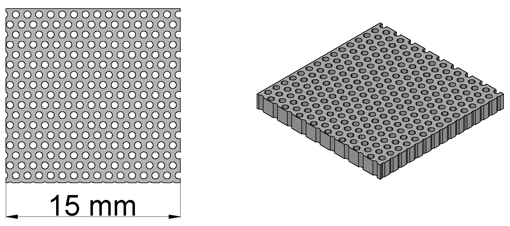
| Lattice Type | (mm) | (mm) | Filling % |
|---|---|---|---|
| - | - | - | 100 |
| square | 1.60 | 0.40 | 81 |
| hexagonal | 1.00 | 0.30 | 68 |
| hexagonal | 1.50 | 0.56 | 50 |
Disclaimer/Publisher’s Note: The statements, opinions and data contained in all publications are solely those of the individual author(s) and contributor(s) and not of MDPI and/or the editor(s). MDPI and/or the editor(s) disclaim responsibility for any injury to people or property resulting from any ideas, methods, instructions or products referred to in the content. |
© 2023 by the authors. Licensee MDPI, Basel, Switzerland. This article is an open access article distributed under the terms and conditions of the Creative Commons Attribution (CC BY) license (https://creativecommons.org/licenses/by/4.0/).
Share and Cite
Alimenti, A.; Torokhtii, K.; Vidal García, P.; Pompeo, N.; Silva, E. Design and Test of a New Dielectric-Loaded Resonator for the Accurate Characterization of Conductive and Dielectric Materials. Sensors 2023, 23, 518. https://doi.org/10.3390/s23010518
Alimenti A, Torokhtii K, Vidal García P, Pompeo N, Silva E. Design and Test of a New Dielectric-Loaded Resonator for the Accurate Characterization of Conductive and Dielectric Materials. Sensors. 2023; 23(1):518. https://doi.org/10.3390/s23010518
Chicago/Turabian StyleAlimenti, Andrea, Kostiantyn Torokhtii, Pablo Vidal García, Nicola Pompeo, and Enrico Silva. 2023. "Design and Test of a New Dielectric-Loaded Resonator for the Accurate Characterization of Conductive and Dielectric Materials" Sensors 23, no. 1: 518. https://doi.org/10.3390/s23010518