
Near-IR & Mid-IR Silicon Photonics Modulators

 , , , , and
Abstract
:1. Introduction
- Highlight state of the art results.
- Focus on new research trends associated with group IV modulators, such as the convergence of photonics and electronics in the C band, the implementation of advanced modulation techniques in the 2 m band and recent emergence of germanium as the platform of choice for mid-IR modulators.
- Discuss areas for further research and improvement.
- Insertion loss (IL)—measured in dB; the total optical loss increase by inserting the device into the optical path.
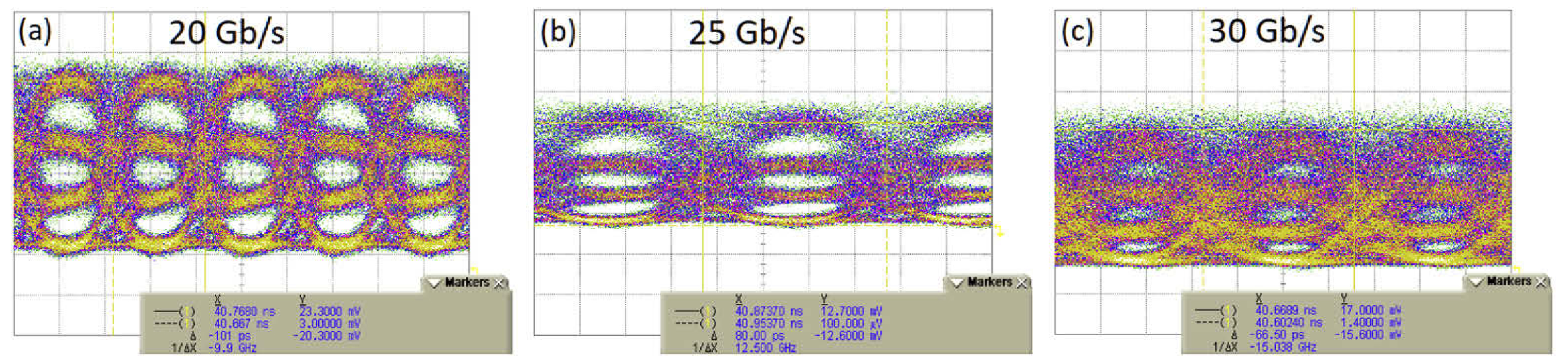
- Modulation speed—measured in Baud; the maximum symbol rate at which the modulator can transmit information.
- Extinction ratio (ER)—measured in dB; the optical intensity of the ‘1’ signal divided by the optical intensity of the ‘0’ signal, also known as modulation depth.
- Modulation efficiency ()—measured in V·cm; the voltage required for a phase shift in a given length.
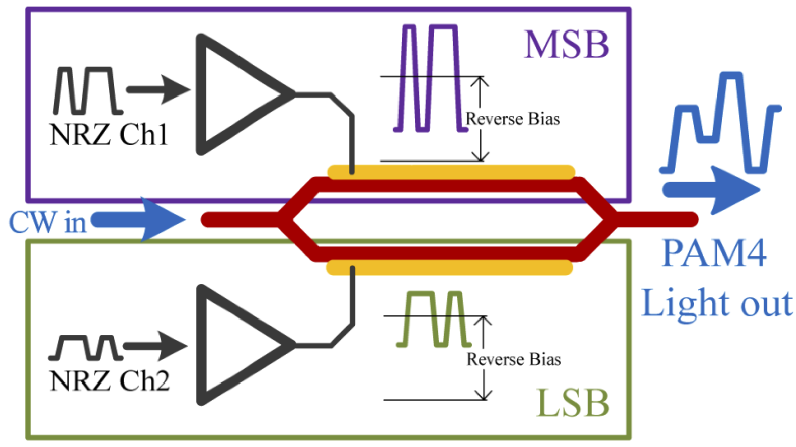
2. Near-IR Group-IV Modulators
3. Mid-IR Group-IV Modulators
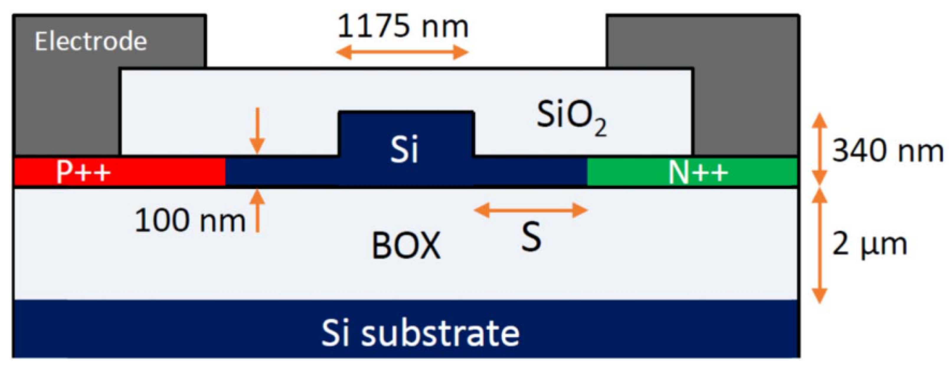
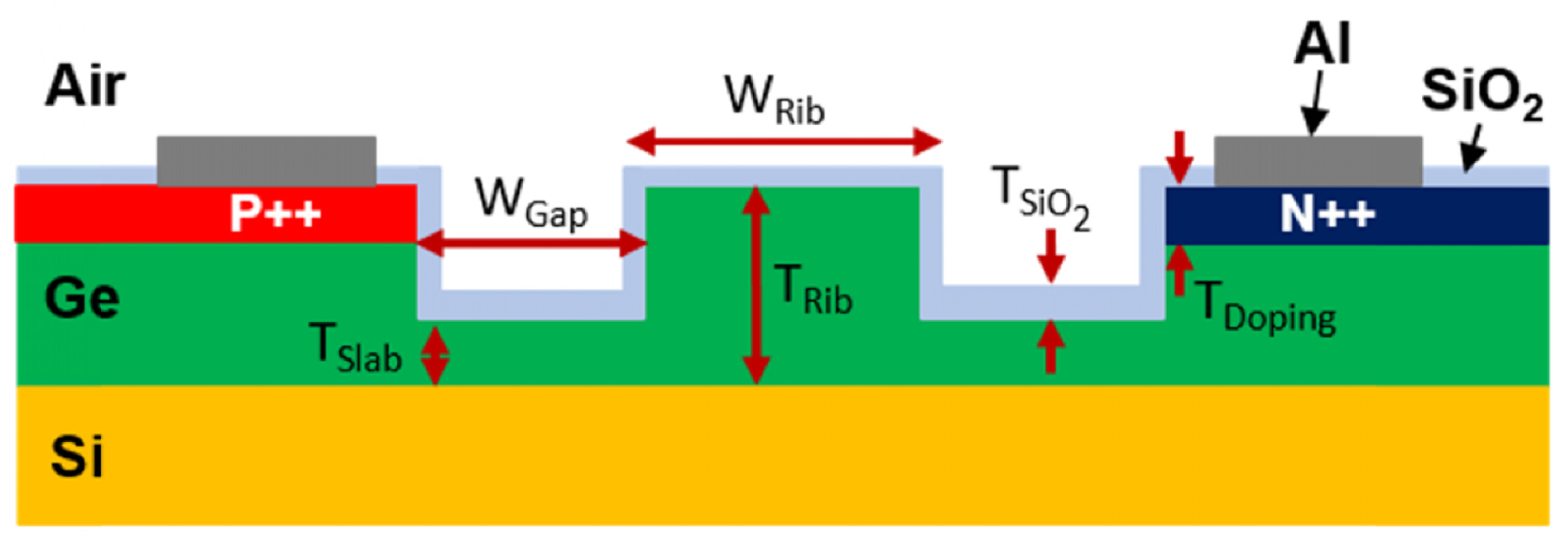
3.1. Modulation in Silicon Waveguides
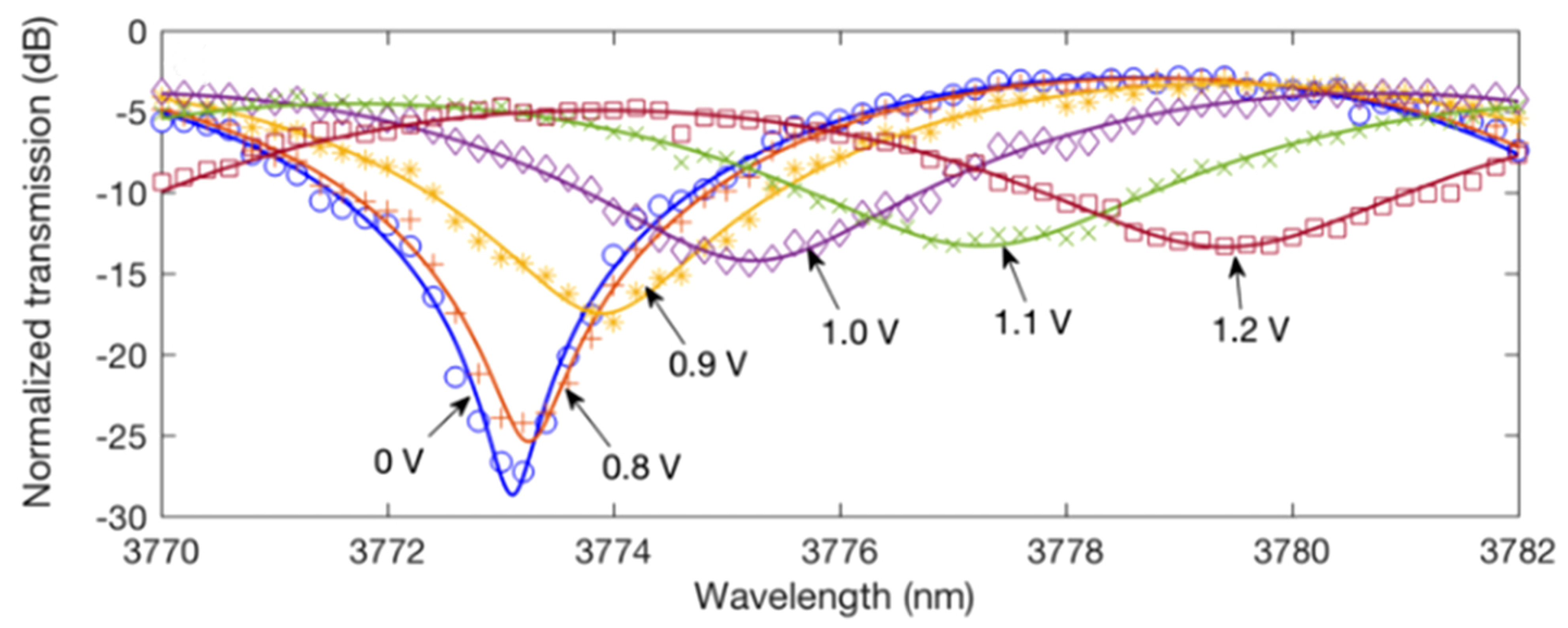
3.2. Modulation in Germanium Waveguides
4. Discussion
5. Conclusions
Author Contributions
Funding
Institutional Review Board Statement
Informed Consent Statement
Data Availability Statement
Conflicts of Interest
Abbreviations
| AC | Alternating current |
| BOX | Burried oxide |
| BP | Black phosphorus |
| BTO | Barium tritanate |
| CMOS | Complementary metal–oxide–semiconductor |
| DAC | Digital to analogue converter |
| DC | Direct current |
| DSP | Digital signal processing |
| EOM | Electro-optical modulator |
| ER | Extinction ratio |
| ERM | Electro-refraction modulator |
| FCA | Free carrier absorption |
| GOI | Germanium on insulator |
| Ge-on-SOI | Germanium on silicon on insulator |
| HC-PBGF | Hollow core photonic bandgap fibre |
| IL | Insertion loss |
| IMDD | Intensity-modulation, direct detection |
| LWIR | Long wave infrared |
| mid-IR | Mid-infrared |
| MIM | Michelson interferometer modulator |
| MOSCAP | Metal-oxide-semiconductor capacitor |
| NRZ | Non return to zero |
| MBE | Molecular beam epitaxy |
| MRM | Microring modulator |
| MZM | Mach-Zehnder modulator |
| near-IR | Near-infrared |
| OOK | On-off keying |
| PZT | Lead zirconate tritanate |
| PAM | Pulse amplitude modulation |
| QW | Quantum well |
| SISCAP | Silicon-insulator-silicon capacitor |
| SMF | Single mode fibre |
| SOI | Silicon on insulator |
| SWIR | Short wave infrared |
| TDFA | Thulium-doped fibre amplifier |
| TO | Thermo optic |
| TPA | Two photon absorption |
| VOA | Variable optical attenuator |
| WDM | Wavelength division multiplexing |
References
- Liu, A.; Jones, R.; Liao, L. A high-speed silicon optical modulator based on a metal-oxide-semiconductor capacitor. Nature 2004, 427, 615–618. [Google Scholar] [CrossRef] [PubMed]
- Reed, G.T.; Jason Png, C. Silicon optical modulators. Mater. Today 2005, 8, 40–50. [Google Scholar] [CrossRef]
- Witzens, J. High-speed silicon photonics modulators. Proc. IEEE 2018, 106, 2158–2182. [Google Scholar] [CrossRef]
- Li, K.; Thomson, D.; Liu, S. 112 GBaud sub pJ/bit integrated CMOS-silicon photonics transmitter. Res. Sq. 2022. [Google Scholar] [CrossRef]
- Zhang, Y.; Zhang, H.; Zhang, J. 240 Gb/s optical transmission based on an ultrafast silicon microring modulator. Photonics Res. 2022, 10, 1127. [Google Scholar] [CrossRef]
- Fathololoumi, S.; Hui, D.; Jadhav, S. 1.6 Tb/s silicon photonics integrated circuit and 800 Gb/s photonic engine for switch co-packaging demonstration. J. Light. Technol. 2021, 39, 1155–1161. [Google Scholar] [CrossRef]
- Rizzo, A.; Daudlin, S.; Novick, A. Petabit-scale silicon photonic interconnects with integrated Kerr frequency combs. IEEE J. Sel. Top. Quantum Electron. 2022, 29, 1–21. [Google Scholar] [CrossRef]
- Cao, W.; Liu, S.; Littlejohns, C.G. High-speed silicon Michelson interferometer modulator and streamlined IMDD PAM-4 transmission of Mach-Zehnder modulators for the 2 um wavelength band. Opt. Express 2021, 29, 14438–14451. [Google Scholar] [CrossRef]
- Wang, X.; Shen, W.; Li, W.; Liu, Y. High-speed silicon photonic Mach-Zehnder modulator at 2 um. Photon. Res. 2021, 9, 535–540. [Google Scholar] [CrossRef]
- Li, T.; Nedeljkovic, M.; Hattasan, N. Ge-on-Si modulators operating at mid-infrared wavelengths up to 8 um. Photon. Res. 2019, 7, 828–836. [Google Scholar] [CrossRef]
- Montesinos-Ballester, M.; Deniel, L.; Koompai, N. Mid-infrared Integrated Electro-optic Modulator Operating up to 225 MHz between 6.4 and 10.7 μm Wavelength. ACS Photonics 2022, 9, 249–255. [Google Scholar] [CrossRef]
- Wang, C.; Zhang, M.; Chen, X.; Bertrand, M. Integrated lithium niobate electro-optic modulators operating at CMOS-compatible voltages. Nature 2018, 562, 101–104. [Google Scholar] [CrossRef] [PubMed]
- He, M.; Xu, M.; Ren, Y. High-performance hybrid silicon and lithium niobate Mach–Zehnder modulators for 100 Gbit s -1 and beyond. Nat. Photonics 2019, 13, 359–364. [Google Scholar] [CrossRef] [Green Version]
- Abel, S.; Eltes, F.; Ortmann, J.E.; Messner, A. Large Pockels effect in micro- and nanostructured barium titanate integrated on silicon. Nat. Mater. 2019, 18, 42–47. [Google Scholar] [CrossRef] [PubMed]
- Alexander, K.; George, J.P.; Verbist, J. Nanophotonic Pockels modulators on a silicon nitride platform. Nat. Commun. 2018, 9, 4–9. [Google Scholar] [CrossRef] [PubMed] [Green Version]
- Kieninger, C.; Kutuvantavida, Y.; Elder, D.L. Ultra-high electro-optic activity demonstrated in a silicon-organic hybrid modulator. Optica 2018, 5, 739. [Google Scholar] [CrossRef] [Green Version]
- Lu, G.W.; Hong, J.; Qiu, F. High-temperature-resistant silicon-polymer hybrid modulator operating at up to 200 Gbit s-1 for energy-efficient datacentres and harsh-environment applications. Nat. Commun. 2020, 11, 1–9. [Google Scholar] [CrossRef]
- Sakib, M.; Liao, P.; Ma, C. A high-speed micro-ring modulator for next generation energy-efficient optical networks beyond 100 Gbaud. In CLEO: Science and Innovations; Optica Publishing Group: Washington, DC, USA, 2021; pp. 6–7. [Google Scholar]
- Posadas, A.B.; Park, H.; Reynaud, M. Thick BaTiO3 epitaxial films integrated on Si by RF sputtering for electro-optic modulators in Si photonics. ACS Appl. Mater. Interfaces 2021, 13, 51230–51244. [Google Scholar] [CrossRef]
- Eltes, F.; Villarreal-Garcia, G.E.; Caimi, D. An integrated optical modulator operating at cryogenic temperatures. Nat. Mater. 2020, 19, 1164–1168. [Google Scholar] [CrossRef]
- Kieninger, C.; Füllner, C.; Zwickel, H. Silicon-organic hybrid (SOH) Mach-Zehnder modulators for 100 GBd PAM4 signaling with sub-1 dB phase-shifter loss. Opt. Express 2020, 28, 24693. [Google Scholar] [CrossRef]
- Thomson, D.; Zilkie, A.; Bowers, J.E. Roadmap on silicon photonics. J. Opt. 2016, 18, 073003. [Google Scholar] [CrossRef]
- Han, J.; Boeuf, F.; Fujikata, J. Efficient low-loss InGaAsP/Si hybrid MOS optical modulator. Nat. Photonics 2017, 11, 486–490. [Google Scholar] [CrossRef] [Green Version]
- Li, Q.; Ho, C.P.; Fujikata, J. Low parasitic capacitance III-V/Si hybrid MOS optical modulator toward high-speed modulation. In Proceedings of the Optical Fiber Communication Conference (OFC) 2020, San Diego, CA, USA, 8–12 March 2020; Volume Part F174, p. 216. [Google Scholar] [CrossRef]
- Thiessen, T.; Grosse, P.; Fonseca, J.D. 30 GHz heterogeneously integrated capacitive InP-on-Si Mach–Zehnder modulators. Opt. Express 2019, 27, 102. [Google Scholar] [CrossRef] [PubMed]
- Webster, M.; Gothoskar, P.; Patel, V.; Piede, D. An efficient MOS-capacitor based silicon modulator and CMOS drivers for optical transmitters. In Proceedings of the IEEE International Conference on Group IV Photonics GFP, Paris, France, 27–29 August 2014; pp. 1–2. [Google Scholar] [CrossRef]
- Li, Q.; Ho, C.; Takagi, S. Optical phase modulators based on reverse-biased III-v/si hybrid metal-oxide-semiconductor capacitors. IEEE Photonics Technol. Lett. 2020, 32, 345–348. [Google Scholar] [CrossRef]
- Sorianello, V.; Midrio, M.; Contestabile, G. Graphene-silicon phase modulators with gigahertz bandwidth. Nat. Photonics 2018, 12, 40–44. [Google Scholar] [CrossRef] [Green Version]
- Talkhooncheh, A.H.; Zhang, W.; Wang, M. A 2.4pJ/b 100Gb/s 3D-integrated PAM-4 optical transmitter with segmented SiP MOSCAP modulators and a 2-channel 28 nm CMOS driver. In Proceedings of the 2022 IEEE International Solid- State Circuits Conference (ISSCC), San Francisco, CA, USA, 20–24 February 2022; pp. 284–286. [Google Scholar] [CrossRef]
- Zhang, W.; Ebert, M.; Li, K. Harnessing plasma absorption in silicon MOS modulators. Nature 2022. preprint. [Google Scholar] [CrossRef]
- Krückel, C.J.; Van Campenhout, J.; van Thourhout, D. Impact of Optical Free-Carrier Generation on the Performance of SOI Phase Shifters. In Proceedings of the 2020 Conference on Lasers and Electro-Optics (CLEO), San Jose, CA, USA, 10–15 May 2020; pp. 1–2. [Google Scholar]
- Li, H.; Balamurugan, G.; Kim, T.; Sakib, M.N.; Kumar, R.; Rong, H.; Jaussi, J.; Casper, B. A 3-D-Integrated Silicon Photonic Microring-Based 112-Gb/s PAM-4 Transmitter With Nonlinear Equalization and Thermal Control. IEEE J. Solid-State Circuits 2021, 56, 19–29. [Google Scholar] [CrossRef]
- Srinivasan, S.A.; Porret, C.; Balakrishnan, S.; Ban, Y. 60 Gb/s waveguide-coupled O-band GeSi quantum-confined Stark effect electro-absorption modulator. In Optical Fiber Communication Conference; Optical Society of America: Washington, DC, USA, 2021; p. 3. [Google Scholar]
- Mastronardi, L.; Banakar, M.; Khokhar, A. High-speed Si/GeSi hetero-structure Electro Absorption Modulator. Opt. Express 2018, 26, 6663. [Google Scholar] [CrossRef]
- Srinivasan, S.A.; Pantouvaki, M.; Gupta, S. 56 Gb/s germanium waveguide electro-absorption modulator. J. Light. Technol. 2016, 34, 419–424. [Google Scholar] [CrossRef] [Green Version]
- Littlejohns, C.G.; Dominguez Bucio, T.; Nedeljkovic, M. Towards a fully functional integrated photonic-electronic platform via a single SiGe growth step. Sci. Rep. 2016, 6, 6–11. [Google Scholar] [CrossRef] [Green Version]
- Srinivasan, S.A.; Porret, C.; Vissers, E.; Favia, P.; De Coster, J.; Bender, H.; Loo, R.; Van Thourhout, D.; Van Campenhout, J.; Pantouvaki, M. High absorption contrast quantum confined Stark effect in ultra-thin Ge/SiGe quantum well stacks grown on Si. IEEE J. Quantum Electron. 2020, 56, 1–7. [Google Scholar] [CrossRef]
- Chaisakul, P.; Marris-Morini, D.; Frigerio, J. Integrated germanium optical interconnects on silicon substrates. Nat. Photonics 2014, 8, 482–488. [Google Scholar] [CrossRef]
- Porret, C.; Srinivasan, S.A.; Balakrishnan, S. O-Band GeSi quantum-confined Stark effect electro-absorption modulator integrated in a 220 nm silicon photonics platform. In Proceedings of the 2020 IEEE Symposium on VLSI Technology, Hilton Hawaiian Village, HI, USA, 16–19 June 2020; pp. 1–2. [Google Scholar] [CrossRef]
- Timurdogan, E.; Sorace-Agaskar, C.; Sun, J. An ultralow power athermal silicon modulator. Nat. Commun. 2014, 5, 1–11. [Google Scholar] [CrossRef] [PubMed] [Green Version]
- Sun, J.; Kumar, R.; Sakib, M.; Driscoll, J. A 128 Gb/s PAM4 silicon microring modulator with integrated thermo-optic resonance tuning. J. Light. Technol. 2019, 37, 110–115. [Google Scholar] [CrossRef]
- Melikyan, A.; Kaneda, N.; Kim, K. Differential drive I/Q modulator based on silicon photonic electro-absorption modulators. J. Light. Technol. 2020, 38, 2872–2876. [Google Scholar] [CrossRef]
- Zhang, H.; Li, M.; Zhang, Y. 800 Gbit/s transmission over 1 km single-mode fiber using a four-channel silicon photonic transmitter. Photonics Res. 2020, 8, 1776–1782. [Google Scholar] [CrossRef]
- Breyne, L.; Ramon, H.; Gasse, K.V. 50 GBd PAM4 transmitter with a 55 nm SiGe BiCMOS driver and silicon photonic segmented MZM. Opt Express 2020, 28, 23950–23960. [Google Scholar] [CrossRef]
- Yong, Z.; Shopov, S.; Mikkelsen, J.C. Flip-chip integrated silicon Mach-Zehnder modulator with a 28 nm fully depleted silicon-on-insulator CMOS driver. Opt Express 2017, 25, 6112–6121. [Google Scholar] [CrossRef]
- Ahmed, A.; Moznine, A.; Lim, D. A dual-polarization silicon-photonic coherent transmitter supporting 552 Gb/s/ wavelength. IEEE J. Solid-State Circuits 2020, 55, 2597–2608. [Google Scholar] [CrossRef]
- Analui, B.; Guckenberger, D.; Kucharski, D. A fully integrated 20-Gb/s optoelectronic transceiver implemented in a standard 0.13-μm CMOS SOI technology. IEEE J. Solid-State Circuits 2006, 41, 2945–2955. [Google Scholar] [CrossRef]
- Sun, C.; Wade, M.T.; Lee, Y. Single-chip microprocessor that communicates directly using light. Nature 2015, 528, 534–538. [Google Scholar] [CrossRef] [PubMed] [Green Version]
- Rito, P.; García López, I.; Petousi, D. A monolithically integrated segmented linear driver and modulator in EPIC 0.25-μm SiGe:C BiCMOS platform. IEEE Transacions Microw. Theory Tech. 2016, 64, 4561–4572. [Google Scholar] [CrossRef]
- Zhou, J.; Wang, J.; Zhu, L. Silicon Photonics for 100 Gbaud. J. Light. Technol. 2021, 39, 857–867. [Google Scholar] [CrossRef]
- Jacques, M.; Xing, Z.; Samani, A. 240 Gb/s silicon photonic Mach-Zehnder modulator enabled by two 2.3-Vpp drivers. J. Light. Technol. 2020, 38, 1. [Google Scholar] [CrossRef]
- Alam, M.; Li, X.; Jacques, M. Net 300 Gbps/λ transmission over 2 km of SMF with a silicon photonic Mach-Zehnder modulator. IEEE Photonics Technol. LeGers 2021, 33, 1391–1394. [Google Scholar] [CrossRef]
- Li, K.; Liu, S.; Thomson, D.J. Electronic–photonic convergence for silicon photonics transmitters beyond 100 Gbps on–off keying. Optica 2020, 7, 1514–1516. [Google Scholar] [CrossRef]
- Sakib, M.; Kumar, R.; Ma, C. A 240 Gb/s PAM4 silicon micro-ring optical modulator. In Proceedings of the Optical Fiber Communication Conference 2022, San Diego, CA, USA, 6–10 March 2022; pp. 11–13. [Google Scholar] [CrossRef]
- Sobu, Y.; Huang, G.; Tanaka, S. High-speed optical digital-to-analog converter operation of compact two-segment all-silicon Mach-Zehnder modulator. J. Light. Technol. 2021, 39, 1148–1154. [Google Scholar] [CrossRef]
- Wang, Y.; Zheng, K.; Song, F.; Tittel, F.K.; Zheng, C. Mid-infrared absorption spectroscopy for gas sensing and application. In Proceedings of the 2020 IEEE 5th Optoelectronics Global Conference (OGC) 2020, Shenzhen, China, 7–11 September 2020; pp. 80–82. [Google Scholar] [CrossRef]
- Murugan, G.S.; Mourgelas, V.; Ahmed, W. Mid-IR spectroscopy: On-chip devices and biodiagnostic applications. In Proceedings of the IEEE 5th International Conference on Emerging Electronics, Vienna, Austria, 8–11 September 2020. [Google Scholar]
- Qi, Y.; Rowe, D.J.; Mittal, V. Integration of mid-infrared SOI photonics with microfluidics. In Silicon Photonics XIV; Reed, G.T., Knights, A.P., Eds.; SPIE: Bellingham, WA, USA, 2019; Volume 10923. [Google Scholar]
- Rowe, D.; Qi, Y.; Nedeljković, M. Microfluidic silicon photonics for aqueous mid-infrared sensing. In Proceedings of the NanoBioTech 2018, Montreux, Switzerland, 29–31 October 2018. [Google Scholar]
- Rowe, D.J.; al Malki, S.; Abduljabar, A.A. Improved split-ring resonator for microfluidic sensing. IEEE Trans. Microw. Theory Tech. 2014, 62, 689–699. [Google Scholar] [CrossRef]
- Essiambre, R.J.; Kramer, G.; Winzer, P.J. Capacity limits of optical fiber networks. J. Light. Technol. 2010, 28, 662–701. [Google Scholar] [CrossRef]
- Soref, R. Group IV photonics: Enabling 2 μm communications. Nat. Photonics 2015, 9, 358–359. [Google Scholar] [CrossRef]
- Roberts, P.J.; Couny, F.; Sabert, H. Ultimate low loss of hollow-core photonic crystal fibres. Opt. Express 2005, 13, 236–244. [Google Scholar] [CrossRef] [PubMed] [Green Version]
- Poletti, F.; Wheeler, N.V.; Petrovich, M.N. Towards high-capacity fibre-optic communications at the speed of light in vacuum. Nat. Photonics 2013, 7, 279–284. [Google Scholar] [CrossRef]
- Slavík, R.; Marra, G.; Fokoua, E.N. Ultralow thermal sensitivity of phase and propagation delay in hollow core optical fibres. Sci. Rep. 2015, 5, 15447. [Google Scholar] [CrossRef] [PubMed] [Green Version]
- Wang, J.; Liang, S.; Kang, Q. Broadband silica-based thulium doped fiber amplifier employing multi-wavelength pumping. Opt. Express 2016, 24, 23001–23008. [Google Scholar] [CrossRef] [PubMed]
- Bjorklund, G.C. Frequency-modulation spectroscopy: A new method for measuring weak absorptions and dispersions. Opt. Lett. 1980, 5, 15–17. [Google Scholar] [CrossRef]
- Soref, R. Mid-infrared photonics in silicon and germanium. Nat. Photonics 2010, 4, 495–497. [Google Scholar] [CrossRef]
- Frey, B.J.; Leviton, D.B.; Madison, T.J. Temperature-dependent refractive index of silicon and germanium. In Optomechanical Technologies for Astronomy; Atad-Ettedgui, E., Antebi, J., Lemke, D., Eds.; International Society for Optics and Photonics, SPIE: Bellingham, WA, USA, 2006; Volume 6273, p. 62732J. [Google Scholar] [CrossRef] [Green Version]
- Nedeljkovic, M.; Stanković, S.; Mitchell, C.J. Mid-infrared thermo-optic modulators in SOI. IEEE Photonics Technol. Lett. 2014, 26, 1352–1355. [Google Scholar] [CrossRef] [Green Version]
- Densmore, A.; Janz, S.; Ma, R. Compact and low power thermo-optic switch using folded silicon waveguides. Opt. Express 2009, 17, 10457–10465. [Google Scholar] [CrossRef]
- Soref, R.; Bennett, B. Electrooptical effects in silicon. IEEE J. Quantum Electron. 1987, 23, 123–129. [Google Scholar] [CrossRef] [Green Version]
- Nedeljkovic, M.; Soref, R.; Mashanovich, G.Z. Free-carrier electrorefraction and electroabsorption modulation predictions for silicon over the 1–14-μm infrared wavelength range. IEEE Photonics J. 2011, 3, 1171–1180. [Google Scholar] [CrossRef]
- Camp, M.A.V.; Assefa, S.; Gill, D.M. Demonstration of electrooptic modulation at 2165 nm using a silicon Mach-Zehnder interferometer. Opt. Express 2012, 20, 28009–28016. [Google Scholar] [CrossRef] [PubMed]
- Cao, W.; Hagan, D.; Thomson, D.J. High-speed silicon modulators for the 2 μm wavelength band. Optica 2018, 5, 1055–1062. [Google Scholar] [CrossRef]
- Wang, W.; Zhang, Z.; Guo, X. Mid-infrared (MIR) Mach-Zehnder silicon modulator at 2 µm wavelength based on interleaved PN junction. In Proceedings of the Conference on Lasers and Electro-Optics, San Jose, CA, USA, 13–18 May 2018; p. STh1B.1. [Google Scholar] [CrossRef]
- Hagan, D.E.; Ye, M.; Wang, P. High-speed performance of a TDFA-band micro-ring resonator modulator and detector. Opt. Express 2020, 28, 16845–16856. [Google Scholar] [CrossRef] [PubMed]
- Chakraborty, U.; Carolan, J.; Clark, G. Cryogenic operation of silicon photonic modulators based on the DC Kerr effect. Optica 2020, 7, 1385–1390. [Google Scholar] [CrossRef]
- Rosenfeld, L.M.; Sulway, D.A.; Sinclair, G.F. Mid-infrared quantum optics in silicon. Opt. Express 2020, 28, 37092–37102. [Google Scholar] [CrossRef]
- Sayers, B.; Rosenfeld, L.; Silverstone, J. Electro-optic Kerr modulation in wide silicon waveguides in the mid-IR. In Proceedings of the 2021 Conference on Lasers and Electro-Optics Europe & European Quantum Electronics Conference (CLEO/Europe-EQEC), Munich, Germany, 21–25 June 2021; p. 1. [Google Scholar] [CrossRef]
- Sepehrian, H.; Yekani, A.; Rusch, L.A. CMOS-photonics codesign of an integrated DAC-less PAM-4 silicon photonic transmitter. IEEE Trans. Circuits Syst. I Regul. Pap. 2016, 63, 2158–2168. [Google Scholar] [CrossRef]
- Nedeljkovic, M.; Littlejohns, C.G.; Khokhar, A.Z. Silicon-on-insulator free-carrier injection modulators for the mid-infrared. Opt. Lett. 2019, 44, 915–918. [Google Scholar] [CrossRef]
- Huang, L.; Dong, B.; Yu, Z. Mid-infrared modulators integrating silicon and black phosphorus photonics. Mater. Today Adv. 2021, 12, 100170. [Google Scholar] [CrossRef]
- Chiles, J.; Fathpour, S. Mid-infrared integrated waveguide modulators based on silicon-on-lithium-niobate photonics. Optica 2014, 1, 350–355. [Google Scholar] [CrossRef] [Green Version]
- Penades, J.S.; Sanchez-Postigo, A.; Nedeljkovic, M. Suspended germanium waveguide for infrared wavelengths. In Proceedings of the 2019 21st International Conference on Transparent Optical Networks (ICTON), Angers, France, 9–13 July 2019; pp. 1–3. [Google Scholar] [CrossRef]
- Gallacher, K.; Millar, R.; Griškevičiūte, U. Low loss Ge-on-Si waveguides operating in the 8–14 μm atmospheric transmission window. Opt. Express 2018, 26, 25667–25675. [Google Scholar] [CrossRef]
- Montesinos-Ballester, M.; Vakarin, V.; Liu, Q. Ge-rich graded SiGe waveguides and interferometers from 5 to 11 μm wavelength range. Opt. Express 2020, 28, 12771–12779. [Google Scholar] [CrossRef] [PubMed]
- Osman, A.; Nedeljkovic, M.; Penades, J.S. Suspended low-loss germanium waveguides for the longwave infrared. Opt. Lett. 2018, 43, 5997–6000. [Google Scholar] [CrossRef] [PubMed]
- Sánchez-Postigo, A.; nux, A.O.M.; Penadés, J.S. Suspended germanium waveguides with subwavelength-grating metamaterial cladding for the mid-infrared band. Opt. Express 2021, 29, 16867–16878. [Google Scholar] [CrossRef] [PubMed]
- Fujigaki, T.; Takagi, S.; Takenaka, M. High-efficiency Ge thermo-optic phase shifter on Ge-on-insulator platform. Opt. Express 2019, 27, 6451–6458. [Google Scholar] [CrossRef]
- Malik, A.; Dwivedi, S.; Landschoot, L.V. Ge-on-Si and Ge-on-SOI thermo-optic phase shifters for the mid-infrared. Opt. Express 2014, 22, 28479–28488. [Google Scholar] [CrossRef]
- Montesinos-Ballester, M.; Liu, Q.; Vakarin, V. On-chip Fourier-transform spectrometer based on spatial heterodyning tuned by thermo-optic effect. Sci. Rep. 2019, 9, 14633. [Google Scholar] [CrossRef] [Green Version]
- Nedeljkovic, M.; Soref, R.; Mashanovich, G.Z. Predictions of free-carrier electroabsorption and electrorefraction in germanium. IEEE Photonics J. 2015, 7, 1–14. [Google Scholar] [CrossRef]
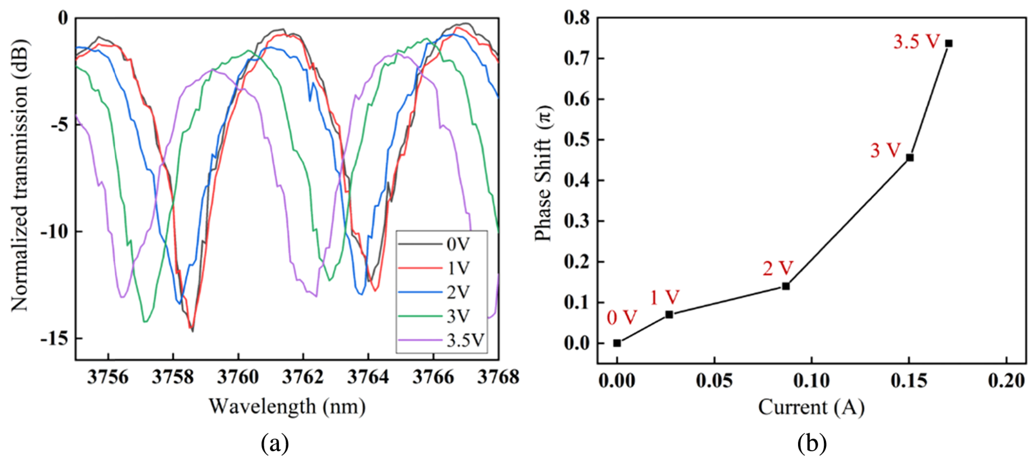
- Zhao, Z.; Ho, C.P.; Li, Q. Efficient mid-infrared germanium variable optical attenuator fabricated by spin-on-glass doping. J. Light. Technol. 2020, 38, 4808–4816. [Google Scholar] [CrossRef]
- Shen, W.; Zhou, G.; Du, J.; Zhou, L.; Xu, K.; He, Z. High-speed silicon microring modulator at the 2 um waveband with analysis and observation of optical bistability. Photon. Res. 2022, 10, A35–A42. [Google Scholar] [CrossRef]


| Work Ref. | Material Platform | Type | Modulation Method | Power Efficiency | Modulation Speed |
|---|---|---|---|---|---|
| [4] | SOI | MZM | Depletion | 0.54 pJ/bit | 112 GBaud 1 |
| [54] | SOI | MRM | Depletion | - | 120 GBaud 1 |
| [29] | SOI | MZM | Accumulation | 2.4 pJ/bit | 50 GBaud 1 |
| [30] | SOI | MRM | Accumulation | - | 100 GBaud 2 |
| [55] | SOI | MZM | Injection | 1.2 pJ/bit | 70 GBaud 1 |
| Work Ref. | Material Platform | Type | IL | ER | Efficiency | Modulation Speed | |
|---|---|---|---|---|---|---|---|
| [8] | SOI | MZM | 1.95 m | 4.96 dB | 6.25 dB | 2.89 V·cm | 25 GBaud 2 |
| [8] | SOI | MIM | 1.95 m | 4.1 dB | 1.97 dB | 1.36 V·cm | 20 GBaud 2 |
| [76] | SOI | MZM | 1.95 m | 3.2 dB | >25 dB 1 | - | 12.5 GBaud 2 |
| [77] | SOI | MRM | 1.97 m | 10–20 dB | 20.1 dB 1 | 2.2–2.6 V·cm | 12.5 GBaud 2 |
| [8] | SOI | MZM | 1.95 m | 4.96 dB | 20 dB 1 | 2.89 V·cm | 12.5 GBaud (PAM-4) 2 |
| [9] | SOI | MZM | 1.95 m | 15 dB | 2.1 dB (@15 GBaud) | 1.6 V·cm | 40 GBaud (PAM-4) 3 |
| [95] | SOI | MRM | 1.95 m | 8 dB | 1.92 dB (@35 GBaud) | 0.85 V·cm | 50 GBaud 3 |
| [82] | SOI | VOA | 3.8 m | 4.96 dB | 34 dB 1 | - | 60 MBaud |
| [82] | SOI | ERM | 3.8 m | 4.96 dB | 22.2 dB 1 | 0.52 V·cm | 125 MBaud |
| [83] | Integrated Si and BP | Waveguide EAM | 3.85 m | - | 5 dB | - | 30 kHz |
| [84] | Integrated Si and LiNbO | MZM | 3.39 m | 3.3 dB | Data | 26 V·cm | 23 kBaud |
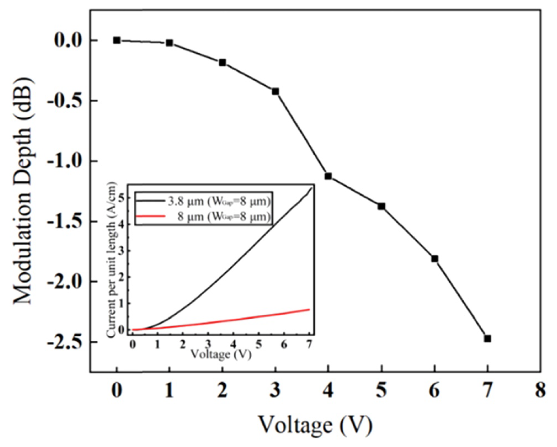
| [10] | Ge on Si | Waveguide EAM | 3.8 m | - | >35 dB 1 | - | 60 MBaud |
| [10] | Ge on Si | MZM | 3.8 m | - | 13 dB | 0.47 V·cm | 60 MBaud |
| [10] | Ge on Si | Waveguide EAM | 8 m | - | 2.5 dB | - | - |
| [11] | Graded SiGe | Waveguide EAM | 10.7 m | 15.6 dB | 1.3 dB | - | 225 MBaud |
| [94] | Ge on insulator | VOA | 1.95 m | - | 20 dB | 380–460 dB/A | - |
Publisher’s Note: MDPI stays neutral with regard to jurisdictional claims in published maps and institutional affiliations. |
© 2022 by the authors. Licensee MDPI, Basel, Switzerland. This article is an open access article distributed under the terms and conditions of the Creative Commons Attribution (CC BY) license (https://creativecommons.org/licenses/by/4.0/).
Share and Cite
Georgiev, G.V.; Cao, W.; Zhang, W.; Ke, L.; Thomson, D.J.; Reed, G.T.; Nedeljkovic, M.; Mashanovich, G.Z. Near-IR & Mid-IR Silicon Photonics Modulators. Sensors 2022, 22, 9620. https://doi.org/10.3390/s22249620
Georgiev GV, Cao W, Zhang W, Ke L, Thomson DJ, Reed GT, Nedeljkovic M, Mashanovich GZ. Near-IR & Mid-IR Silicon Photonics Modulators. Sensors. 2022; 22(24):9620. https://doi.org/10.3390/s22249620
Chicago/Turabian StyleGeorgiev, Georgi V., Wei Cao, Weiwei Zhang, Li Ke, David J. Thomson, Graham T. Reed, Milos Nedeljkovic, and Goran Z. Mashanovich. 2022. "Near-IR & Mid-IR Silicon Photonics Modulators" Sensors 22, no. 24: 9620. https://doi.org/10.3390/s22249620