1. Introduction
In the last decade, the accelerated development of photonic integrated circuits (PICs) based on silicon-compatible materials has been mainly driven by the need to develop devices that can fulfil the high demands of optical communications and data interconnects in the near-infrared (NIR) [
1,
2,
3]. However, as the integrated platforms have matured, the use of PICs have broadened to applications in which some of the intrinsic properties of silicon pose a challenge. As a result, there has been an increased interest in exploring different CMOS compatible materials that can complement the functionality of silicon, such as amorphous silicon, silicon oxynitride, silicon nitride, aluminium nitride (AlN) and alumina (Al
2O
3) [
4,
5,
6,
7,
8].
Amongst these materials, silicon nitride (SiN) is a mature CMOS compatible platform that has gained significant attention for the demonstration of linear, nonlinear and active integrated photonics devices [
9] due to its flexible optical properties that can be tailored for a wide range of integration schemes and applications. SiN is suitable for broadband applications since it has a wide optical bandgap (2.7–5 eV) that sets the lower limit of its transparency window to the ultraviolet (UV) regime extending it all the way to the mid-infrared ( 5
). The material also offers a compromise between level of integration and flexible dimension control as it has a modest refractive index that can be tuned between 1.7 and 3.1 to provide a good optical confinement in the near-infrared (NIR) with a high tolerance to both surface roughness and dimensional variations that enable one to attain ultralow propagation losses [
10,
11,
12]. Additionally, it has a low thermo-optic coefficient (
), which makes it attractive for the realisation of devices that are highly sensitive to temperature variations. Finally, it exhibits a third-order Kerr nonlinearity with negligible two-photon absorption (TPA) in the NIR which makes it suitable for nonlinear applications.
This review article presents the recent progress on the integration of the SiN platform in a variety of interesting research areas. This includes the demonstration of waveguides with sub-dB propagation losses in the C-band ( 1550 nm) for all-optical processing and the use of custom SiN films with a high silicon concentration to achieve large Kerr coefficients for nonlinear optics. Additionally, it covers the integration of SiN with a range of materials such as electro-optic polymers, lithium niobate (LN), barium titanate oxide (BTO), graphene, TMD semiconductors and transparent conducting oxides (TCOs) to demonstrate optical modulators. It further discusses the integration of SiN with phase change materials (PCMs) and a postfabrication device trimming technique as strategies to achieve nonvolatile photonic devices. Finally, it incorporates the integration of III-V materials and SiN waveguides as a means to achieve efficient lasers on a silicon substrate. The vast subject of sensing and in particular gas sensing and biological sensing, which is the subject of intense research for chemical functionalisation and sensing through evanescent field interaction, is not covered in this review as it has been covered extensively elsewhere [
13,
14].
2. Low-Loss Silicon Nitride Materials
SiN films are typically deposited using either high-temperature low-pressure chemical vapour deposition (LPCVD) or low-temperature plasma-enhanced chemical vapour deposition (PECVD). Both methods rely on chemical reactions in the gas form that result in hydrogenated amorphous films with a composition that tends to depart from the stoichiometric form of the material (Si3N4). Hence, these films are characterised by the presence of hydrogen bonds (Si-H and N-H), which act as absorption centres that can lead to undesirable losses in the NIR, particularly in the C-band centred at 1550 nm. The main difference between the two methods is that LPCVD layers are deposited at high temperatures (>800 °C), while PECVD films are deposited at much lower temperatures (<400 °C).
Although PECVD films enable the back-end-of-line integration with materials that are sensitive to temperature, layers deposited through LPCVD are by far preferred for the growth of SiN films for single-layer photonic integrated circuits since high quality layers with a high density and high uniformity can be achieved with a relatively low processing cost and high throughput. Moreover, high-temperature LPCVD processes have the energy required to break the hydrogen bonds that can increase the optical losses in the NIR, enabling the realisation of devices with losses <1 dB/cm.
In fact, LPCVD SiN waveguides with ultralow propagation losses <
dB/
at 1550 nm and a record low loss of
dB/
at 1580 nm have been demonstrated since 2011 [
15,
16,
17]. To achieve these results, the typical strip waveguide geometry that provides a moderate optical confinement with a thickness ranging between 200 and 400 nm needs to be replaced with a high aspect ratio geometry with a thickness below 100 nm. By using such a geometry, the optical confinement of the waveguide is reduced allowing more than 85% of the mode to travel in the SiO
2 cladding. Therefore, the large mode area reduces the scattering losses by minimising the mode interaction with the sidewall roughness of the waveguide, allowing a decrease of the propagation losses from values close to 1 dB/cm attained with the moderate confinement geometry to the sub-dB scale [
18,
19,
20].
Although the low-confinement approach drastically reduces the propagation losses of the waveguides, it increases the footprint of the fabricated devices since radii >5 mm are required to reduce the bending losses. As a result, waveguides with a small effective area and high confinement are necessary to enable tighter bends for large scale photonic integrated systems [
21,
22]. Furthermore, they are critical to achieve high optical intensity, dispersion engineering for nonlinear processes and a reduced birefringence to potentially allow for the fabrication of polarisation-independent devices [
18,
21,
22].
However, as the modes within such thick waveguides are highly localised in the core, both the intrinsic losses of the material and the scattering losses produced at the interfaces of the waveguide have a stronger impact than radiation losses on the minimum propagation losses that can be realised. Moreover, the growth of SiN layers with thickness >400 nm poses a fabrication challenge as they tend to crack due to the tensile stress of the material, especially if they are deposited with a high-temperature LPCVD process [
23].
Several approaches have been proposed to demonstrate thick SiN layers with low propagation losses. As previously discussed, the propagation losses are the result of the scattering losses that occur due to surface roughness, the absorption produced chemical impurities and defects within the material, and the radiation losses directly related to the confinement of the light. Most of the proposed methods focus on reducing the absorption losses of the material layer and the scattering losses through advanced fabrication techniques, since the radiation losses of the highly confined geometries tend to be negligible. In this section, we discuss some of the methods that have been used to achieve losses <1 dB/cm and <2 dB/cm using LPCVD and PECVD SiN layers.
2.1. Thermal Cycling
Since 2013, Lipson et al. have demonstrated a subtractive method based on thermal cycling and stress relieving mechanical trenches to produce stoichiometric Si
3N
4 layers with thickness up to 910 nm on 100 mm oxidised silicon wafers (
Figure 1). In this approach, the stress of the films is alleviated by mechanically scribing a series of trenches on the top SiO
2 surface around the edges of the wafer [
24]. These trenches prevent the formation of cracks that can propagate across the wafer, creating crack-free regions in which photonic devices can be fabricated.
The growth of the LPCVD layer is performed in a multistep process to minimise the internal stress of the layers. Firstly, a 350 nm film is deposited and then annealed at 1200 °C for 3
in an Ar atmosphere to reduce its hydrogen concentration in order to minimise its absorption losses. Afterwards, both steps are repeated to reach the required thickness [
22]. The top roughness of the surface layer can be further reduced by means of a chemical mechanical polishing step (CMP) before patterning the devices using electron beam lithography (EBL) and inductively coupled plasma reactive ion etching (ICP-RIE) using a CHF
3/O
2/N
2 chemistry [
22,
25]. Finally, to minimise the contribution of the cladding to the propagation loss of the devices, the wafer is cladded with a 250 nm layer of high-temperature oxide (HTO) followed by 2
of PECVD oxide. Using this fabrication method, the authors have not only demonstrated thick Si
3N
4 films with low-thickness nonuniformity <1%, but they have realised 1800 × 910 nm waveguides with propagation losses as low as
dB/cm at 1550 nm [
22,
24].
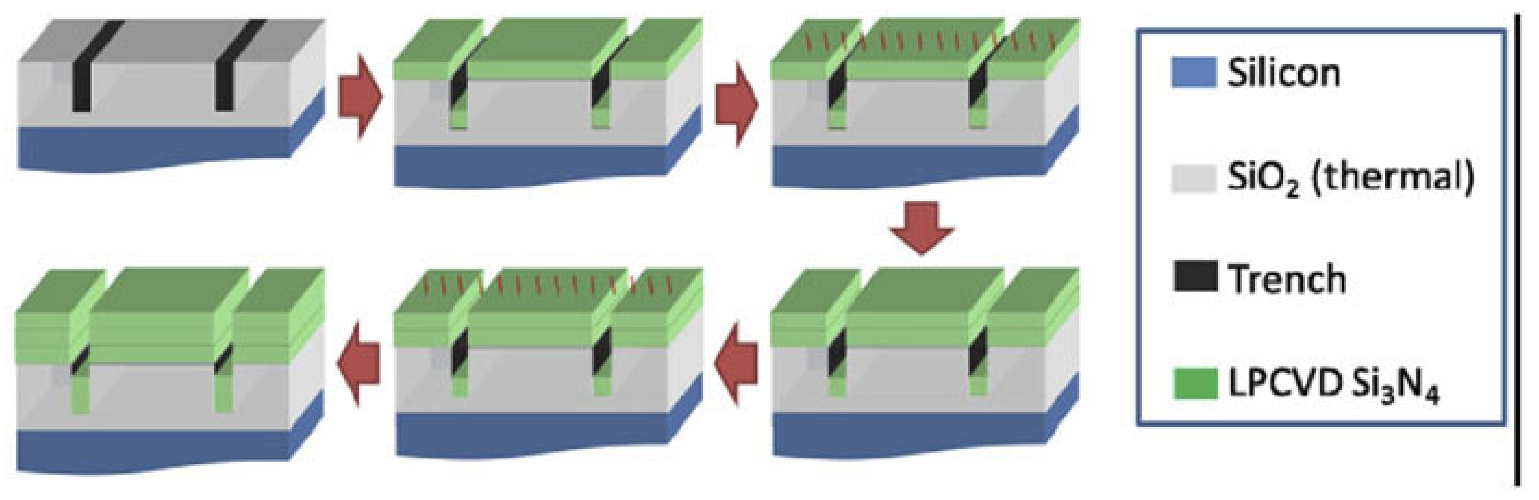
2.2. Photonic Damascene Reflow Process
In 2015, Epping et al. introduced an innovative additive fabrication process that can be used to fabricate waveguides with a thickness up to 900 nm by depositing a thick Si
3N
4 layer into trenches patterned on a 100 mm thermally oxidised wafer [
26]. After further optimisation, this method evolved into the photonic Damascene reflow process illustrated in
Figure 2 [
27,
28,
29,
30]. In this technique, waveguide trenches and a dense stress-release pattern are written onto a wafer by means of EBL and photolithography. The full pattern is then etched through reactive ion etching (RIE) using a thin amorphous silicon layer as a sacrificial hard mask which is then stripped. Before depositing the Si
3N
4 film, a reflow step of the oxide preform is performed by heating the substrate at 1250 °C to reduce the sidewall roughness, which can introduce additional scattering losses without deforming the waveguide. The LPCVD Si
3N
4 film with a thickness up to
is then deposited in order to fill completely the previously etched trenches. The device waveguides are then obtained by removing the excess Si
3N
4 by means of CMP to achieve a planar and polished surface. Once the waveguides are obtained, the wafer is annealed at 1150 °C to reduce the absorption losses of the material. Finally, the substrate is cladded with a layer of tetraethyl orthosilicate (TEOS) followed by a low-temperature oxide layer (LTO). This optimised method has allowed the demonstration of 2000 × 600 nm waveguides with propagation losses of
dB/cm at 1550 nm [
29]. Furthermore, this process has been further optimised to provide high-yield and full wafer-scale fabrication of low-loss devices on 100 mm substrates [
21]. To achieve this, EBL has been replaced by DUV stepper lithography, which enables the increase of the throughput and the reproducibility of the process. Additionally, an etch-back process based on dry etching and CMP has been introduced to decrease the wafer-scale thickness variation of the Si
3N
4 layer (<3%).
2.3. Multistep Annealing
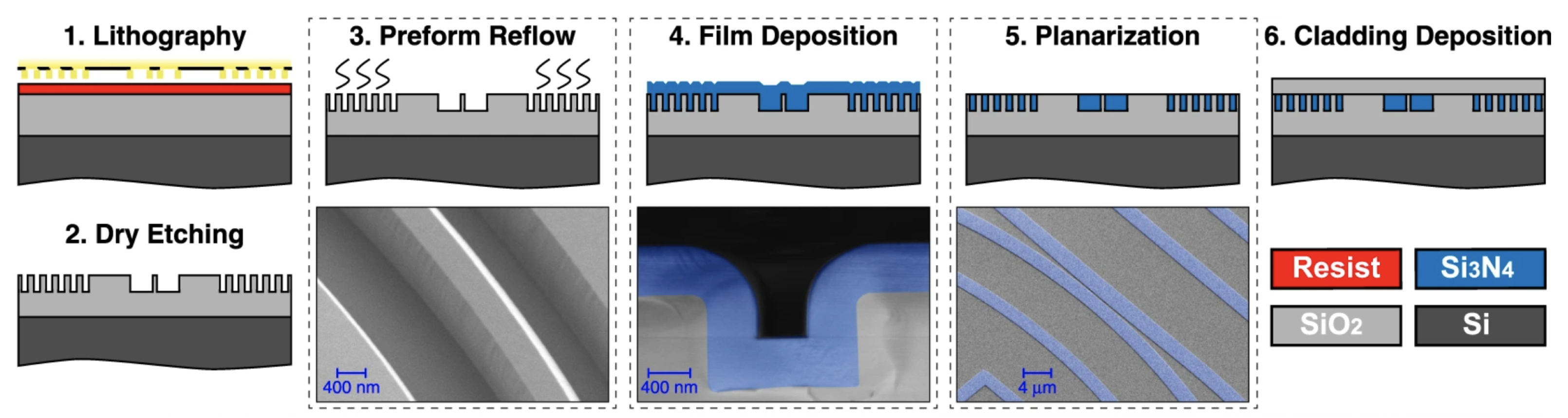
In 2018, Ye et al. proposed another subtractive fabrication method illustrated in
Figure 3, that relies on multiple annealing steps to achieve films with thicknesses >600 nm on 76 nm silicon wafers with a 3
thermal oxide [
31]. In this method, the stress-release trenches and the thermal cycling process described previously are adopted to reduce the crack formation. After transferring the stress-release pattern with direct laser writing, the Si
3N
4 layer is deposited in an LPCVD furnace in two steps, in between which the deposited film is annealed at 1100 °C for 3
in a N
2 ambient to minimise its hydrogen content. Later on, the devices are patterned on the layer by means of EBL and ICP-RIE with a CHF
3/O
2 chemistry. After etching, the wafer is annealed again at 1100 °C for 3
in N
2 to further reduce the hydrogen. The waveguides are then covered with a 500 nm layer of low-pressure TEOS deposited at 710 °C which is then annealed at 1100 °C in N
2 to increase its density. Finally, the devices are cladded with 2
of PECVD oxide. Following this method, the authors have realised 1800 × 645 nm waveguides with propagation losses of
dB/cm at 1550 nm [
31]. Furthermore, amongst the methods described previously, this technique has been the only one that has demonstrated Si-rich SiN waveguides of a cross-section of 1850 × 600 nm, exhibiting propagation losses of
dB/cm at 1550 nm [
32].
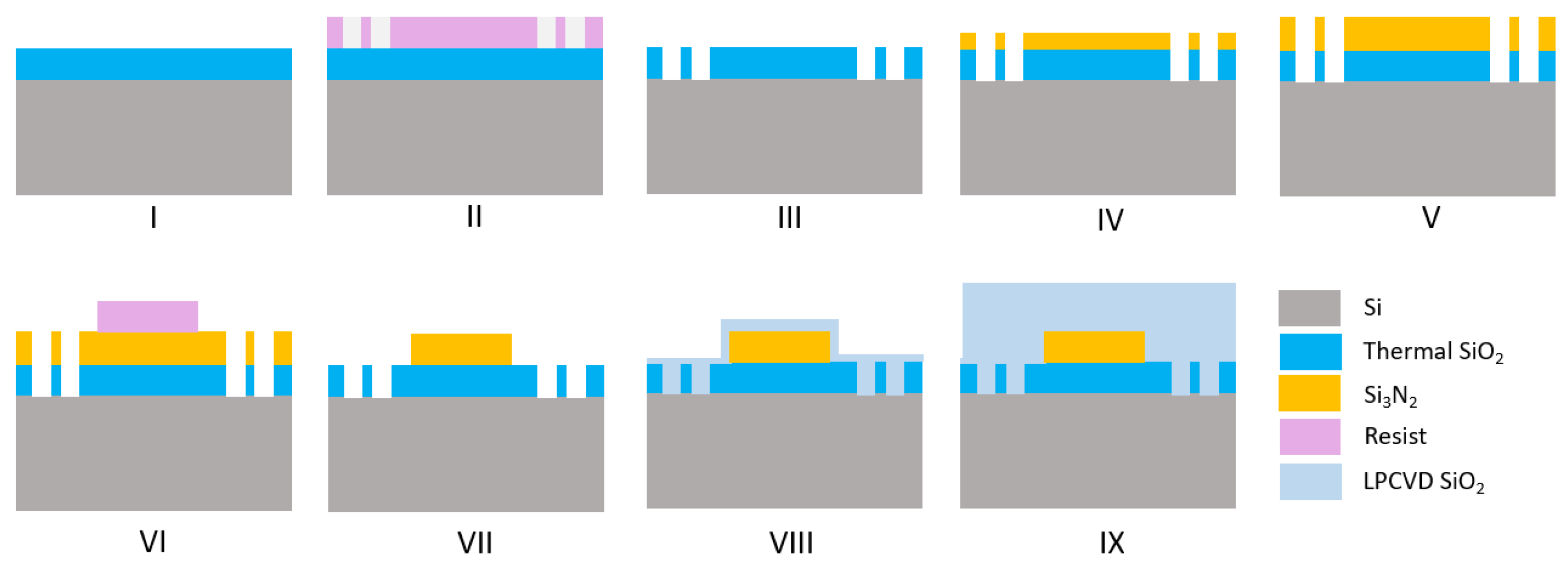
2.4. Twist-and-Grow
In 2018, El Dirani et al. developed a deposition technique known as twist-and-grow illustrated in
Figure 4, that has been used to produce thick Si
3N
4 layers (>1
) in a standard large-format fabrication line [
33]. The fabrication begins with a blanket 200 mm silicon substrate with a 3
thermal oxide layer, on which a 800 nm thick Si
3N
4 film is deposited in two steps using the twist-and-grow technique [
34,
35]. In this method, the layers are deposited by means of LPCVD at 780 °C with a deposition rate of <2 nm/min that enables the production of films with minimal hydrogen content. In between steps, the wafer is cooled down to 630 °C to eliminate stress-related cracks and rotated by 45° to redistribute the uniaxial stress that can significantly bow the wafer. The wafer then goes through a CMP step to reduce the surface roughness before patterning the waveguides using DUV lithography and inductively coupled plasma etching (ICP) with a tailored CF
4/CHF
3/Ar that minimises sidewall roughness. The resist and any etching residues are removed with an O
2 plasma and the surface is cleaned with a H
2SO
4 solution before selectively etching the Si
3N
4 on the backside of the wafer to alleviate the tensile stress that can appear after patterning to ensure that the wafer can continue its fabrication in the process line. In order to reduce the propagation losses, the patterned wafer is annealed at 1100 °C for a few minutes in H
2 to smoothen the sidewalls, at 1200 °C in O
2 to encapsulate the waveguides with a native oxidation to reduce scattering centres, and at 1200 °C for 3
in N
2 to drive out the hydrogen impurities that contribute to the absorption of the material in the NIR. As a last step, the waveguides are encapsulated with a TEOS and a LTO layer deposited by high-density plasma-enhanced chemical vapour deposition (HDP-ECVD). Using this fabrication process the authors have not only demonstrated 1600 × 800
waveguides with propagation losses of
dB/cm at 1560 nm [
33], but they have also demonstrated a largely scalable process with high reproducibility that has potential for applications that require thicker layers.
2.5. Summary
Table 1 summarises the main features of the processes that have been used to demonstrate SiN layers with losses in the sub-dB/cm regime. All these methods have achieved losses <
dB/cm by applying a combination of stress-release patterns, multistep deposition processes, multiple annealing steps and CMP planarisation. However, although they provide very low losses, none of these techniques are compatible with the CMOS back-end-of-line which is necessary to achieve the multilayer integration required for more complex photonic integrated circuits, as they all have steps with high-processing temperatures (>400 °C). Moreover, all the methods have mostly focused on optimising the Si
3N
4 stoichiometric composition (n = 2.0), except for the multistep annealing process that has also demonstrated low-loss Si-rich SiN films (n = 2.07). This narrow range of refractive indices poses limitations for nonlinear applications that require higher refractive indices to achieve stronger nonlinear effects [
11,
36] and for the demonstration of devices operating at shorter telecom wavelengths which often benefit from lower refractive indices to minimise propagation losses and phase errors [
37,
38].
3. Si-Rich Silicon Nitride for Nonlinear Photonics
Variation of the gas composition of the film-forming reactants during the silicon nitride (SiN) deposition process affects not only the linear part of the refractive index, but also the nonlinear part. This provides an additional degree of freedom in the design of all-optical signal processing devices based on third-order (Kerr) nonlinear effects [
39,
40,
41]. Si-rich SiN layers of a varying refractive index can be grown by increasing the amount of SiH
during the material deposition process. As reported in the literature [
39,
42], an increase in the silicon concentration allows a greater nonlinear Kerr coefficient to be realised, however, at the expense of typically higher absorption losses. Therefore, a proper material composition can be selected depending on the specific requirements of the target application. For example, low-loss (
dB/cm ) Si-rich SiN with a refractive index of 2.07 at 1550 nm (slightly greater than that of stoichiometric Si
3N
4) was used to fabricate microresonators with high quality factors (Q ∼
) in the C and L bands, allowing the generation of broadband coherent frequency combs in this platform [
32]. On the other hand, despite its higher propagation losses (3–10 dB/cm), ultra-silicon-rich nitride (USRN, refractive index equal to 3.1 at 1550 nm) emerged as a promising platform for the development of highly compact nonlinear devices operating at low optical power levels, thanks to its nonlinear refractive index being two orders of magnitude greater than that of stoichiometric Si
3N
4 [
36,
43,
44,
45,
46,
47].
Table 2 summarises the main features of several Si-rich SiN platforms, with different refractive indices, demonstrated in the literature. In the following subsections, we report the most recent developments in Si-rich SiN-based nonlinear optics, focusing our attention on some specific examples showcasing the flexibility of this material platform for the design of nonlinear devices, manifested by the tunability of its linear and nonlinear optical properties.
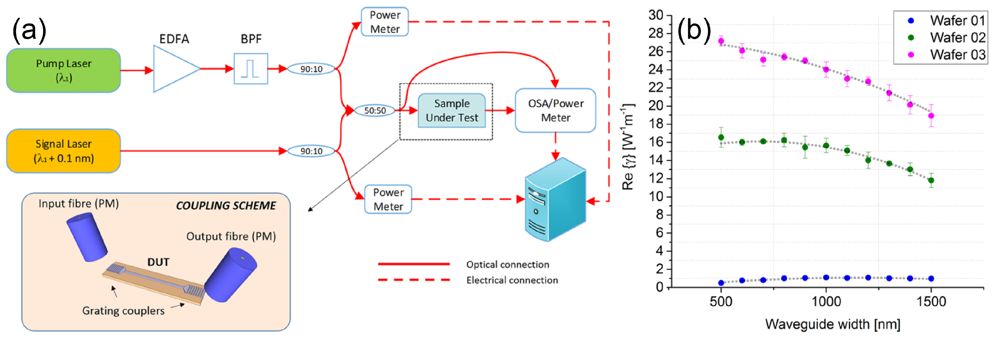
3.1. Tunable Nonlinear Optical Properties
We review here a comprehensive experimental study to show the dependence of the nonlinear optical properties on the Si-rich SiN material composition [
39]. Specifically, the nonlinear performance of three layers deposited on a thermal SiO
substrate with different refractive index was investigated, whose properties are summarised in
Table 3. Fully etched waveguides with different widths (in the range 0.5–1.5
m) were written onto the different layers and characterised in the measurement campaign. Light coupling with optical fibres was achieved by means of grating couplers (GCs) and tapered edge-couplers (ECs).
The third order nonlinear response of an optical waveguide can be generally expressed in terms of the nonlinear parameter
:
where
is the angular frequency,
is the nonlinear refractive index,
c is the speed of light,
is the effective area and
is the two-photon absorption (TPA) coefficient. The real part of Equation (
1) (also known as
) describes the Kerr response of the optical waveguide and introduces a nonlinear phase shift to the propagating light. The imaginary part of the Equation (also known as
) represents the TPA response, that accounts for the power-dependent nonlinear losses that the optical signal undergoes during propagation. The values of
for the different Si-rich SiN layers were experimentally measured by using a continuous-wave (CW) four-wave-mixing (FWM)-based scheme [
39], whose experimental setup is shown in
Figure 5a. A pump laser (wavelength
=
nm, optical power ranging from 20 mW to 2
at the waveguide input GC) was amplified by a polarisation-maintaining Erbium-doped fibre amplifier (PM-EDFA) and then was sent to an optical band pass filter (BPF) to filter out the EDFA-generated amplified spontaneous emission (ASE) noise. A 50:50 fibre coupler was employed to combine the pump with a weaker CW optical signal (the signal optical power was always kept at least 10 dB below the pump power level) generated by a tunable external cavity laser (ECL). GCs were used to couple the two optical waves into the waveguides under test. A FWM-induced idler at a new frequency was generated in the waveguide and the three signals were coupled back to a PM fibre by means of an output GC. By recording optical spectra for different pump power levels, the
coefficients of the fabricated waveguides were derived using the following equation:
where
and
are the idler and signal optical powers measured at the waveguide output, respectively,
is the pump power at the waveguide input,
is the nonlinear effective length and
accounts for the phase-mismatch resulting from chromatic dispersion [
49]. In the considered case, since the signal and pump waves were placed relatively close to each other in wavelength (
<
nm), the effect of dispersion can be neglected and it is therefore possible to consider
= 1.
The results of the nonlinear measurement campaign are reported in
Figure 5b. It can be seen that layers 02 and 03 show around an order of magnitude greater nonlinear Kerr response than layer 01. The reason for this enhancement can be found in the increased material nonlinearities resulting from the presence of additional Silicon in the material composition. Specifically, by increasing the silicon concentration, the linear refractive index of the material increases and this is accompanied by an increase in the nonlinear Kerr coefficient as well, in line with the empirical rule developed by Miller [
50].
The imaginary part of the nonlinear coefficient,
, was then measured by means of pulse-transmission experiments [
39,
51]. A fibre mode-locked laser centred at 1550 nm (pulse duration:
; repetition rate: 20 MHz) was employed as the light source. Unlike the previously described CW experiments, the light was coupled in and out of the integrated waveguides by using tapered ECs, in order not to impose any spectral distortion on the laser pulses. The TPA coefficients
of the various Si-rich SiN layers were estimated by measuring the average power at the waveguide output as a function of the input peak power. Under the assumption of a hyperbolic-secant pulse temporal profile (which is the nominal pulse shape of the optical source used in these experiments), the average output power
can be expressed as a function of the input peak power
through the following equations [
51]:
where
is the average input power,
is the propagation loss coefficient and
L is the waveguide physical length. TPA coefficients
(and hence
) for the three Si-rich SiN layers were derived using Equations (
3) and (
4) and the measured values for three different waveguide widths (500, 700 and 1000 nm) are reported in
Table 4.
The experimental results showed that both layers 01 and 02 were not significantly affected by TPA-related losses, even when relatively high optical power levels (>10 peak power) were employed. Conversely, when the silicon content in the material was further increased (as in the case of layer 03), TPA-related effects started to appear, suggesting that this Si-rich SiN composition was not suitable for high-power low-loss applications.
3.2. FWM-Based Frequency Conversion in Multimode Si-Rich Silicon Nitride Waveguides
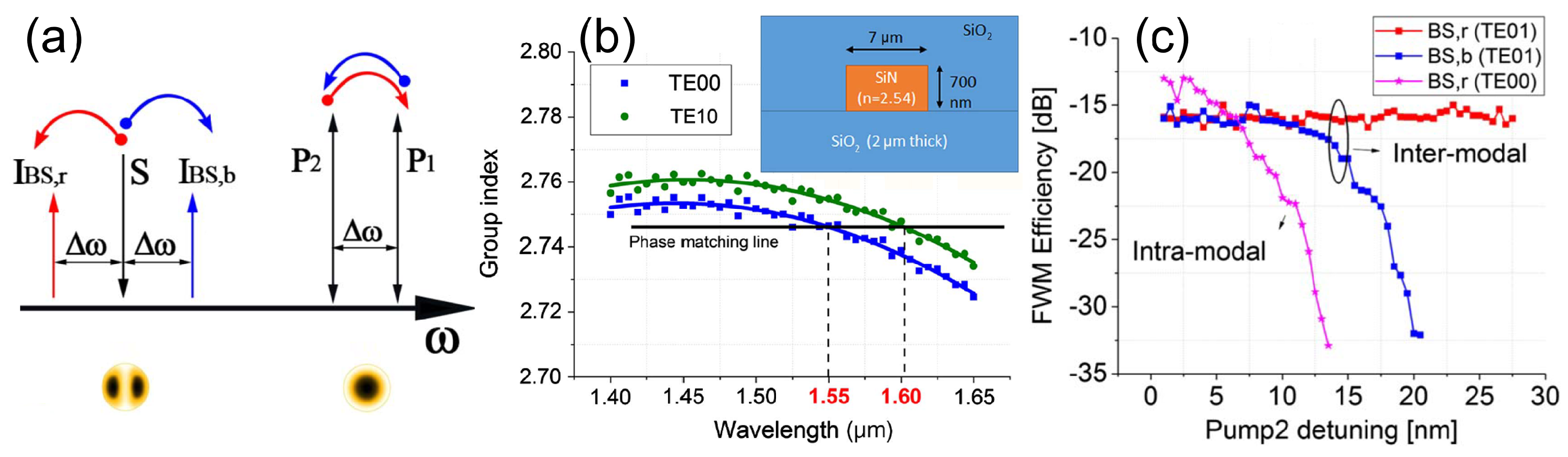
The discussion in the previous section has shown that Si-rich SiN layers can be properly engineered to obtain a high Kerr nonlinear response with no TPA-related losses. This allows waveguides to be operated at Watt-power levels, unlike silicon itself, which is strongly limited by TPA-related effects.
In this configuration, the two pumps were placed into the TE00 mode of the waveguide, while the signal and the generated idlers were in the TE10 mode. As in any FWM-based process, efficient nonlinear conversion takes place only when the phase-matching condition among the different waves is satisfied. In particular, efficient IM-BS-FMW can be achieved over a wide bandwidth whenever the inverse group velocity curve of one mode is a frequency-shifted replica of the other mode [
52]. The propagation properties of the two modes were engineered by acting on two parameters: the waveguide cross-section and the refractive index of the core Si-rich SiN material. As shown in
Figure 6b, the phase-matching condition between the TE00 and TE10 modes can be satisfied over a large bandwidth by considering
= 1550 nm and
= 1601 nm. Moreover, this waveguide design can be used to efficiently suppress one idler in order to have a unidirectional FWM process. In fact, one limitation of the BS-FWM mechanism is its bidirectionality, which can result in the generation of unwanted idlers at new frequencies [
53,
54]. Numerical simulations confirmed that by setting
at a fixed wavelength equal to 1550 nm and changing the pump-to-pump separation
by varying the position of
, it is possible to achieve a constant conversion efficiency for
for a large
detuning range (>50 nm). Conversely, the generation of
is hindered in this scenario, and it takes place only over a narrow
range [
40]. A measurement campaign was also carried out, whose results are shown in
Figure 6c. The wavelengths of the two pumps were initially set at
= 1550 nm and
= 1551 nm, while the signal wavelength was set at
=
nm. The IM-BS-FWM conversion efficiency was measured for
and
by gradually detuning
towards longer wavelengths. As predicted by numerical simulations, the conversion efficiency of
remained constant at a value of around
dB across a large
detuning range, while
was no longer detectable for a
detuning value equal to 20 nm.
3.3. Nonlinear Optics in Ultra-Silicon-Rich Nitride Platform
Ultra-Silicon-rich Nitride (USRN) is typically grown at a low temperature ( 250 °C) using inductively coupled chemical vapour deposition and is characterised by a high silicon content compared to nitrogen (Si
N
), with a refractive index equal to 3.1 at 1550 nm [
36,
43]. The nonlinear optical properties of this material were characterised by open and closed aperture z-scan measurements [
55]. A nonlinear refractive index
equal to
/
was measured at 1550 nm, which is 100× larger than the
value of stoichiometric Si
3N
4 [
56,
57] and more than 10× larger than the
value of all the other Si-rich SiN platforms reported in the literature (see
Table 2 for comparison). This allows the realisation of highly efficient and compact nonlinear devices, with a total waveguide length shorter than 1 cm, operating at low optical power levels. However, the high silicon concentration makes it particularly challenging to achieve low propagation losses compared to the case of Si-rich SiN compositions with lower refractive indices. Open aperture z-scan measurements showed that TPA is absent in the C-band, with three-photon absorption being the dominant contributor to nonlinear losses. The high linear and nonlinear refractive index of USRN allows one to achieve high values for the waveguide nonlinear parameter (
equal to 500
for a waveguide cross-section of 0.30 × 0.55
2 [
43]), making it possible to obtain large nonlinear conversion/amplification at relatively low pump power levels [
36]. For example, an optical parametric gain of
dB was demonstrated using a pulsed pump and a CW signal by degenerate-FWM in a high-optical-confinement USRN waveguide (
dB/cm propagation losses) operating in the anomalous dispersion regime in the 1550 nm wavelength region [
43]. Cascaded FWM with gain down to the third generated idler was also observed, with peak parametric gains measured for the first, second and third idlers equal to 36.2, 21.2 and
dB, respectively. A further enhancement of the material nonlinearity was achieved by exploiting the slow-light effect in USRN photonic crystal waveguides, with the demonstration of an optical parametric gain per unit length of 333 dB/cm [
58]. In this study, FWM experiments were carried out with a pulsed pump and a CW signal in a 97
long USRN photonic crystal waveguide (22 ± 2 dB/cm propagation losses in the slow light region) with a measured optical parametric signal gain and idler conversion efficiency of 3 dB and
dB, respectively. The nonlinear efficiency of the USRN material was also proven in the observation of temporal soliton dynamics, specifically in the soliton-effect temporal compression and fission of optical pulses [
48,
59]. High-order solitons are generated in optical media characterised by the simultaneous presence of anomalous dispersion and nonlinearity, and they evolve periodically during propagation, experiencing a temporal narrowing at the beginning of each soliton period. This property can be used to realise strong temporal compression of optical pulses, which allows the generation of ultrashort pulses and the increase of the pulses’ peak powers. Then, the high-order soliton compression process was exploited to achieve a 8.7× temporal compression of 2
optical pulses using a low pulse energy equal to ∼16
in a 7 mm long USRN waveguide (characterised by 3 dB/cm propagation losses) [
48]. To the best of our knowledge, this is the largest soliton-effect temporal compression demonstrated on an integrated photonic waveguide to date. Wideband nonlinear spectral broadening of input fs laser pulses based on self-phase modulation was also demonstrated in USRN add-drop ring resonators (broadening factor of two) and waveguides (broadening factor of around three per 1 mm length) [
46]. More recently, thermo-optically tunable nonlinear spectral broadening was reported using an USRN device consisting of a 3 mm long cladding-modulated Bragg grating and a 7 mm long channel waveguide. An increase in the bandwidth of the output pulse spectrum from 69 to 106 nm was measured by decreasing the temperature from 70 °C to 25 °C [
60]. Wide supercontinuum generation exceeding 0.6 of an octave at 1550 nm was also demonstrated in a 7 mm long USRN waveguide using 500 fs optical pulses [
61].
While several demonstrations of FWM-based nonlinear applications were reported in USRN waveguides using pulsed pumps, the propagation losses of this platform are still too high to allow efficient CW-FWM experiments in centimetre-long waveguides. Opportunities to further improve this material platform and reduce the propagation losses exist, such as the adoption of established protocols for low-loss Si
3N
4 waveguide fabrications such as high temperature annealing or the use of the photonic Damascene reflow process. In order to reduce Si-H and N-H bonds-related losses, recipes that make use of alternative gases other than silane could be investigated. For example, the use of dichlorosilane gas (SiH
Cl
) already showed promising results towards a further optimisation of this material platform [
62,
63]. The reduction of the propagation losses in combination with the large Kerr coefficient of the USRN platform could allow the demonstration of efficient CW-operated phase-sensitive parametric amplifiers and frequency combs with sub-
threshold power.
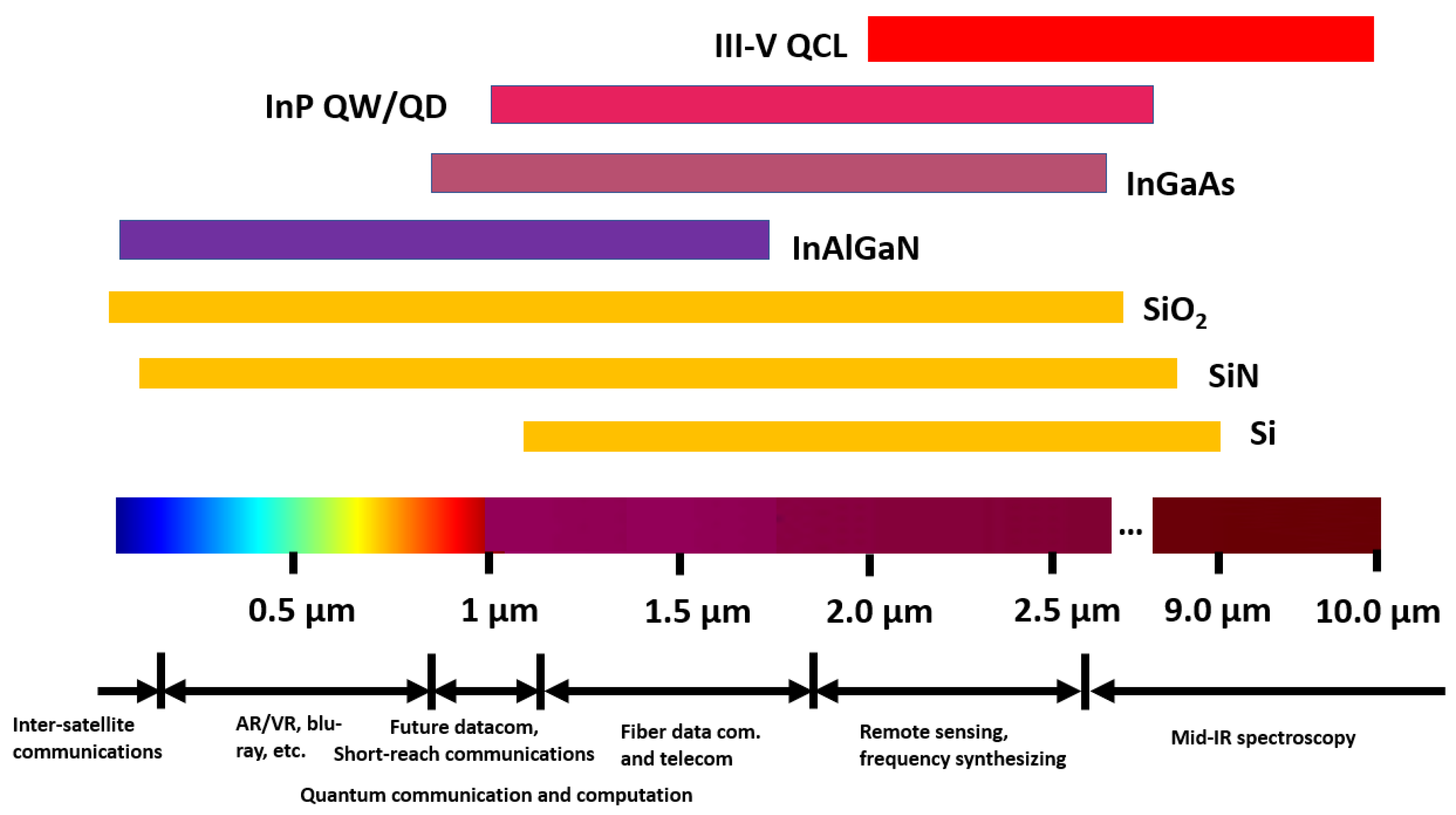
6. III-V/SiN Integration: Towards Efficient Monolithic Lasers on Silicon Substrate
The explosive growth of silicon-based photonic integrated circuits (PICs) along with their wide applications requires high-performance coherent light sources lasers. Current commercialised silicon PICs are mainly powered by external free-running semiconductor lasers, [
222,
223] substantially increasing the cost of the systems, the power requirements and limiting scalability. In order to satisfy a range of systems, the integration of lasers to CMOS PICs requires a number of specifications such as a high output power, low lasing threshold, high temperature stability, ultralow linewidth and low noise level. Because of the indirect bandgap of Si, the heterogeneous or monolithic integration of lasers based on direct-bandgap III-V materials is currently the preferred solution for silicon PICs [
224]. This is despite substantial progress related to the lasers based on group-IV SiGeSn materials which have been demonstrated at low temperatures and mid-infrared wavelengths [
225,
226,
227]. Currently, most III-V laser integration schemes are based on the silicon-on-insulator (SOI) platforms [
228,
229], focusing on wavelengths in the near- and mid-infrared (NIR and MIR) regions, owing to the transparency window of Si (
Figure 9). In contrast, silicon nitride (SiN) possesses a wider transparency window, extending from the MIR down to the UV, due to the large bandgap of the material. This matches the available bandgap of III-V semiconductor families (
Figure 9). As discussed previously, due to the SiN benefits from an extremely low thermo-optic coefficient [
230,
231], nonlinear coefficient [
232], tunable refractive index (by adjusting the Si/N ratio) [
10,
216] and CMOS-fabrication compatibility, ultralow-loss (<
dB/cm) SiN is quickly becoming an ideal candidate for a range of applications in silicon photonics [
8,
41]. In contrast, III-V lasers integrated with SiN waveguides (III-V/SiN lasers) have yet to be developed fully, to compete with the widely reported III-V/Si lasers [
228,
229]. In this section, we focus on the recent progress achieved in III-V lasers (represented by GaN, InP and GaAs) along with their major characteristics required for CMOS PICs.
As the most obvious material advantage compared with that of Si-, SiN-coupled lasers can extend working wavelengths down to the visible–NIR wavelength range below 1100 nm, where virtual reality (VR)/augmented reality (AR), high-density optical storage, short-reach communication, and quantum technologies play important roles (
Figure 9) [
233,
234,
235]. An example of the benefits offered by integration in SiN was demonstrated by Kumari and colleagues, who employed a SiN-based high-index-contrast subwavelength grating (HCG) to substitute one of the distributed Bragg reflectors (DBRs) of a GaAs VCSEL working at 850 nm, via adhesive die bonding [
236]. The grating structure not only worked as a cavity mirror, but it also guided light into the horizontal direction (perpendicular to the DBR stacks) out of the cavity. Following this, they fabricated an intracavity polarisation-insensitive HCG coupler followed by a SiN waveguide. By adjusting the parameters of the grating (duty cycle/period) and the oxide aperture size (4–6
m), the laser exhibited a low threshold of only
mA and maximum single mode suppression ratio (SMSR) of 55 dB at ~845 nm [
237,
238,
239]. At a shorter wavelength range, a violet-blue (405–435nm) RR with high quality factor (Q) up to
using low-loss (
dB/cm) SiN waveguides have been fabricated (
Figure 10a,b) [
240], and a conceptual blue III-Nitride/SiN PIC has been proposed by employing vertical grating couplers (with a maximum simulated coupling efficiency of 40%) and adiabatic optical tapers (with simulated coupling loss <4 dB), respectively, [
241]. In addition to the progress in the visible–NIR wavelength range, SiN also demonstrates its versatility in the MIR region, where photonic devices and integrated systems with performances comparable to their Si counterparts have been developed [
242]. Nevertheless, III-V/SiN lasers targeting the MIR region have not been reported so far, which is in contrast with progresses reported on the development of MIR III-V/Si lasers [
242,
243]. Besides a wider transparency window, III-V/SiN-coupled lasers also have a better thermal stability compared with III-V/Si lasers, which is crucial for the wavelength tuning stability in PICs. For example, Iadanza and colleagues demonstrated a single mode laser (with SMSR = 45 dB) with a III-V gain chip coupled to an external SiN DBR waveguide [
244]. The laser exhibited extreme thermal stability with mode-hop-free behaviour under an injection current range of 15–62mA from room temperature up to 80 °C. The authors attributed the improved lasing properties to the low thermal-optical coefficient of SiN [
230,
231]. The above-mentioned reports on III-V/SiN lasers with excellent photonic characteristics prove that they can bring added functionalities of CMOS PICs to III/Si lasers, by extending the working wavelength to a wider range.
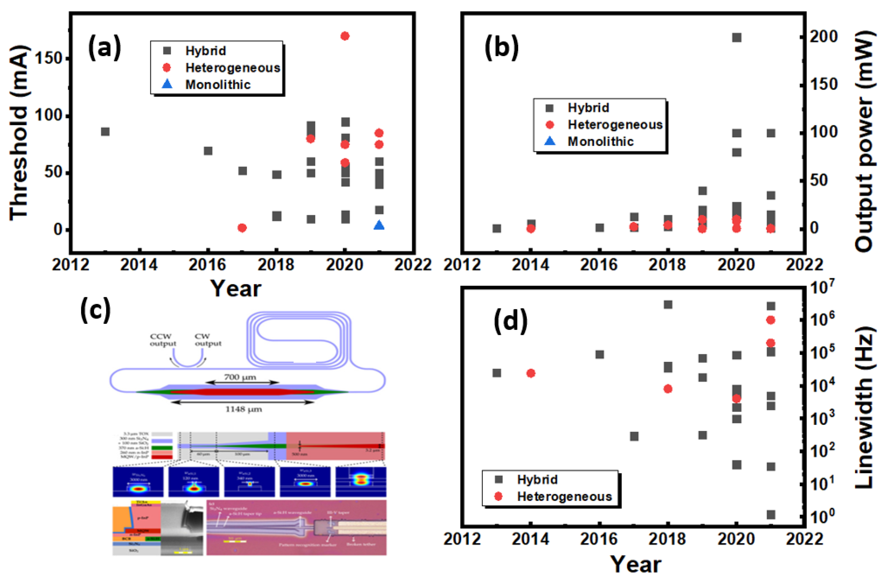
Figure 11a shows the recent progress related to the integration methods of on-chip lasers coupled with SiN waveguides [
239,
244,
245,
246,
247,
248,
249,
250,
251,
252,
253,
254,
255,
256,
257,
258,
259,
260,
261,
262,
263,
264,
265,
266,
267,
268,
269,
270,
271,
272,
273,
274,
275,
276,
277,
278,
279,
280]. Except for those labelled in
Figure 11a,b, almost all lasers are coupled to the SiN platform with mature or commercial InP gain structures (DFB, reflective semiconductor optical amplifier, FP, etc.) [
281] by hybrid or heterogeneous integration. In general, the hybrid integration, utilising easily controlled edge-/butt-coupled schemes to merge bulky SiN platforms and a separate III-V gain chip, gives a better threshold and output power (
Figure 11a,b), while the III-V gain is often homoepitaxially grown on a non-Si substrate. This method often leads to a large footprint not favoured by CMOS PICs. Both heterogeneous (wafer-/die-level gain area transfer) and monolithic (III-V grown directly on Si) integration are more promising, even though they are at an early stage of maturity. It is worth to mention that sophisticated optical couplers are often required for heterogeneous/monolithic III-V lasers owing to the large difference in the refractive index between SiN and III-Vs (>1.1 at 1550 nm).
Figure 11c shows an optical taper that consists of a III-V/Si intermediate layer/SiN layer used in a single-frequency laser, to couple light from the gain region into SiN ring waveguides, generating a threshold current of 59 mA and on-chip output power of
mW [
245]. Such couplers, developed since the first heterogeneous III-V/SiN laser [
265], are subject to coupling losses from sub-dB to several dB and can be further improved by structural design and material engineering. It is also noticeable that a majority of integrated lasers in recent years are based on InP (
Figure 11a,b) [
281], regardless of the fact that GaAs lasers have a higher quantum efficiency and a better thermal conductivity. Recent advances in telecom-wavelength lasing based on high-gain GaAs QDs heteroepitaxially grown on Si and SOI substrates with low thresholds and high temperature stability [
282], indicate that it is a promising gain material for III-V/SiN monolithic integration and there is a strong possibility that 100 mW level heterogeneous/monolithic III-V/SiN lasers are achievable in the near future.
The narrow linewidth of a laser that is often associated with low noise, is an important metric for the integration with the Si PICs towards practical applications in communications [
286], LIDAR [
287], spectroscopy [
288] and optical clocks [
289]. Traditional DBR or DFB lasers utilise intracavity feedback from the cavity mirrors, which normally realise a megahertz-level linewidth [
290,
291]. In contrast, a III-V/SiN-coupled laser is a natural external cavity configuration, whose lasing dynamics can be analysed by the same theory as that of an external cavity semiconductor laser [
292], where the linewidth reduction is one of the major advantages. The linewidth of an external cavity laser can be calculated from,
, where
is the cavity linewidth,
A and
B are parameters related to phase (increasing group delay and photon lifetime) and spectral feedback of the external cavity (related threshold gain and local carrier density) [
293]. Benefiting from the fast-developing SiN devices, especially resonators with Q up to >200 M [
294], a highly precise phase (factor A) and spectral (factor B) feedback [
295,
296] is achievable in addition to an extended cavity length (thereby reducing
), likely to generate ultranarrow linewidth.
Figure 11d displays the state-of-the-art linewidth of III-V/SiN-coupled lasers in terms of integration method [
244,
246,
248,
249,
252,
254,
256,
257,
258,
261,
262,
263,
264,
266,
267,
270,
272,
273,
274,
275,
276,
279,
280,
283,
284,
285]. It appears that significant progress has been made with hybrid integration when compared to heterogenous/monolithic integration, though the latter started its development at a later stage. The best results reported so far show that a hertz-level linewidth on a III-V/SiN laser is achievable with hybrid integration [
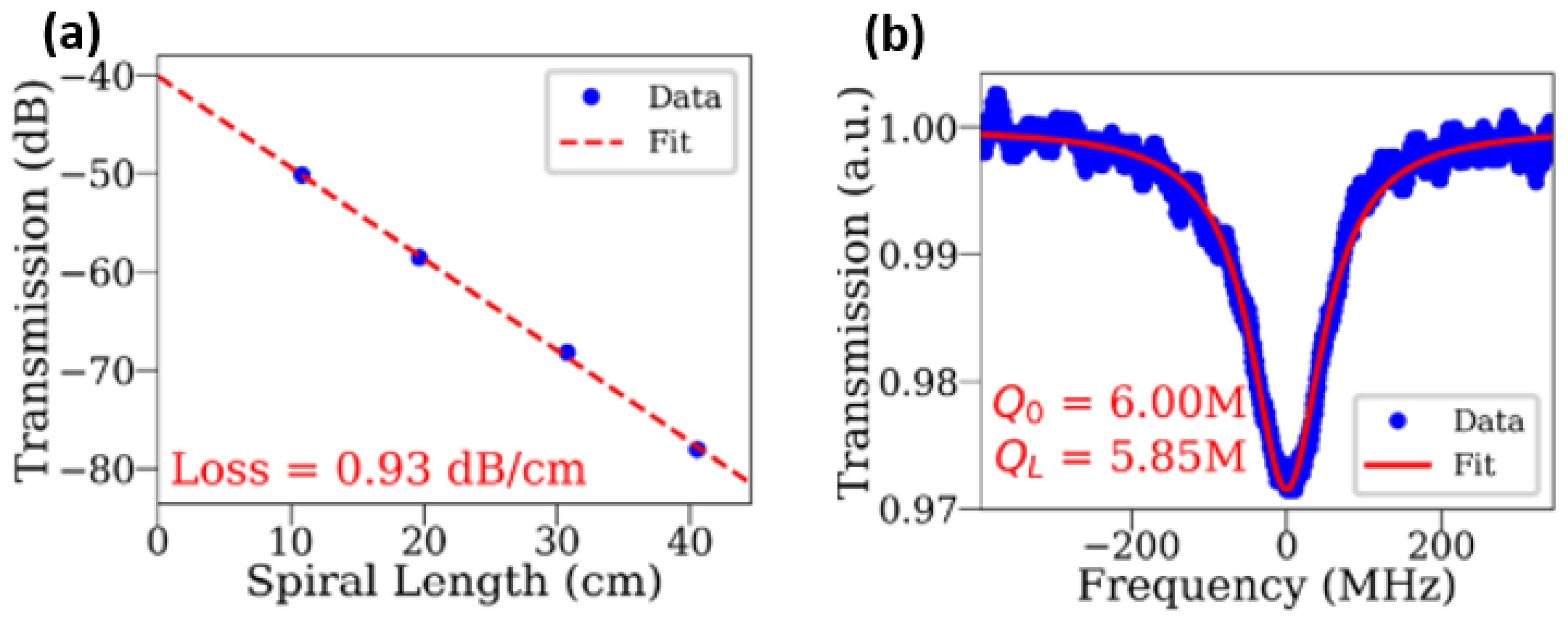
283], which is the record value regarding III-V and Si photonics integrated platforms. The authors utilised ultrahigh Q (170 M–270 M) microresonators externally coupled to a III-V DFB laser based on high-aspect-ratio SiN waveguides ( 100 nm in thickness and
–8
in width). By precisely controlling the feedback phase from the SiN resonator to the active region (to adjust the air gap between chips), self-injection-locking was achieved. They observed a record narrow linewidth of
Hz along with low frequency noise of
Hz
/Hz. Though this is an example of a hybrid integrated laser, ultralow linewidth with low noise could also be achievable using heterogenous/monolithic III-V/SiN-coupled lasers with a smaller footprint, given that the technical barriers only lie in the III-V crystal quality on Si and the III-V/SiN interface engineering.
In summary, we reviewed the progress of III-V/SiN lasers associated with their performance and fabrication methods. The III-V/SiN-coupled lasers have arisen as a strong competitor to III-V/Si lasers, due to their advantages in terms of their extended transparency window down to UV–visible range and their better thermal stability. Based on the above discussions, it is concluded that the state-of-the-art integration technologies of III-V/SiN lasers are at very different stages. To date, the III-V/SiN laser with high performance (e.g., low threshold, high output power, narrow linewidth) are mainly fabricated by hybrid or heterogeneous integration with a relatively large footprint and some back-end type CMOS compatibility. The more recent and still challenging monolithic integration is also gaining attention, [
259,
260,
297] and has a great potential for dramatically reducing the costs by fully leveraging the CMOS economy of scale and pushing further the limits of very large scale integrated photonics (VSLI-P) [
298].


 ,
, 


