Article

Metamaterial-Integrated High-Gain Rectenna for RF Sensing and Energy Harvesting Applications †

Department of Electrical and Computer Engineering, University of Florida, Gainesville, FL 32611, USA
*
Author to whom correspondence should be addressed.
This paper is an extended version of our abstract presented in a conference: Lee, W.; Kim, H.; Hwang, S.; Jeon, S.; Cho, H.; Yoon, Y.-K. 3D integrated high-gain rectenna in package with metamaterial superstrates for high efficiency wireless power transfer applications. In Proceedings of the 2021 IEEE 71st Electronic Components and Technology Conference (ECTC), Virtual Meeting, 1 June–4 July 2021; pp. 1317–1322.
Sensors 2021, 21(19), 6580; https://doi.org/10.3390/s21196580
Submission received: 31 August 2021 / Revised: 26 September 2021 / Accepted: 27 September 2021 / Published: 1 October 2021

Abstract

:
This paper presents a metamaterial (MTM)-integrated high-gain rectenna for RF sensing and energy harvesting applications that operates at 2.45 GHz, an industry, science, medicine (ISM) band. The novel MTM superstrate approach with a three-layered integration method is firstly introduced for rectenna applications. The integrated rectenna consists of three layers, where the first layer is an MTM superstrate consisting of four-by-four MTM unit cell arrays, the second layer a patch antenna, and the third layer a rectifier circuit. By integrating the MTM superstrate on top of the patch antenna, the gain of the antenna is enhanced, owing to its beam focusing capability of the MTM superstrate. This induces the increase of the captured RF power at the rectifier input, resulting in high-output DC power and high entire end-to-end efficiency. A parametric analysis is performed in order to optimize the near-zero property of the MTM unit cell. In addition, the effects of the number of MTM unit cells on the performance of the integrated rectenna are studied. A prototype MTM-integrated rectenna, which is designed on an RO5880 substrate, is fabricated and characterized. The measured gain of the MTM-integrated rectenna is 11.87 dB. It shows a gain improvement of 6.12 dB compared to a counterpart patch antenna without an MTM superstrate and a maximum RF–DC conversion efficiency of 78.9% at an input RF power of 9 dBm. This results in the improvement of the RF–DC efficiency from 39.2% to 78.9% and the increase of the output DC power from 0.7 mW to 6.27 mW (a factor of 8.96 improvements). The demonstrated MTM-integrated rectenna has shown outstanding performance compared to other previously reported work. We emphasize that the demonstrated MTM-integrated rectenna has a low design complexity compared with other work, as the MTM superstrate layer is integrated on top of the simple patch antenna and rectifier circuit. In addition, the number of MTM units can be determined depending on applications. It is highly envisioned that the demonstrated MTM-integrated rectenna will provide new possibilities for practical energy harvesting applications with improved antenna gain and efficiency in various IoT environments.

1. Introduction

With the development of wireless technologies, the ambient wireless power density is growing owing to the increasing number of electromagnetic (EM) power sources. Harvesting this radio frequency energy has gained a lot of attention in recent years. A rectenna (rectifier + antenna), which is the key component of the wireless RF energy harvesting, continues to be a highly expected solution to the power challenges related to ubiquitous sensor connectivity as envisioned in the Internet of Things (IoT). Rectennas with a high-gain antenna and a high-efficiency rectifier are highly required.
Recently, various rectenna designs have been proposed in the literature for RF energy harvesting, such as monopole rectennas [1,2], dipoles [3,4,5], circularly polarized (CP) antennas [6,7,8], dual-band rectennas [9,10], and a broadband rectenna [11]. In order to solve the limited power challenges, researchers have studied various techniques for improving the gain of the rectenna, such as reflecting surface [4,12], differential microstrip [13], differential feeding [14], antenna array [15,16], SIW cavity [17], air gap [9], and aperture coupling [9,18]. In [12], a 5.8 GHz high-gain dual-rhombic-loop rectenna was investigated to achieve an antenna gain of 10.7 dBi. By having a dual-rhombic-loop antenna structure with terminated gaps, left-hand circular polarization was achieved. The maximum RF–DC conversion efficiency was 80% at an input power of 20 dBm. This dual-rhombic-loop structure had an advantage of high gain and broadband properties, but the improved gain was still limited, and an integrated rectifier made the entire system large. In [13], a differential microstrip antenna with a gain of 8.5 dBi was introduced. The differential antenna was utilized in either center-grounded or differential configuration. The rectenna was designed to operate at the GSM900 band (890–960 MHz), with a peak RF–DC conversion efficiency of 65% at an input power of 2.19 dBm. However, a two-layered differential patch antenna with the additional ground layer made the design complexity very high. In [16], a monopole wideband fractal antenna array fed by a microstrip-to-slot-line transition feeding network was designed. As the feeding line was based on slot-line stubs and radial microstrip, the broadband microstrip-to-slot-line transitions were realized. An antenna gain of 8.5 dBi and RF–DC conversion efficiency of 76% at 5 dBm were obtained. This fractal antenna array had an advantage of broadband property (0.91 to 2.55 GHz), but the design process of the fractal antenna array increased the design complexity. In addition, the rectifier was connected to the antenna in a perpendicular direction, thereby increasing the overall dimension of the rectenna and limiting its practical applicability. In [17], a 24 GHz substrate integrated waveguide (SIW) cavity-backed antenna array was demonstrated for millimeter-Wave energy harvesting. By having the SIW cavity in the antenna, the gain was increased from 10.3 dBi to 12.6 dBi. The maximum RF–DC conversion efficiency was 42% at 12.55 dBm. Even though the gain of the demonstrated antenna was relatively high, the measured RF–DC conversion efficiency was too low, and the overall normalized device was comparably large (0.776 λ3). Moreover, the SIW cavity made the fabrication and design process more difficult. In [9], a microstrip patch antenna with a right-angle triangular aperture slot was exhibited. By having an air gap between the patch antenna and feed line, the improved antenna gain was realized. An antenna gain of 7.82 dBi and an RF–DC conversion efficiency of 32.5% at 10 dBm were obtained, but the rectifier circuit was not integrated to the antenna, thereby increasing overall system size, as the rectifier was connected to the same layer of antenna. Overall, the improved antenna gains of the previously reported work were still limited, and the methods to enhance the gain highly increased the device complexity. Therefore, a fully integrated rectenna with high gain, low design complexity, and high RF–DC conversion efficiency is needed.
In the meantime, some researchers have introduced metamaterials (MTMs) for the antenna gain improvement as a form of MTM superstrates [19,20,21,22], where MTM superstrates help increase the antenna gain by utilizing the near-zero refraction characteristic of the MTM. MTMs are artificially designed materials that have uncommon EM properties, such as evanescent wave amplification, negative refraction, and near-zero refraction, thereby improving the antenna gain [23,24]. Figure 1 shows the principle of a gain improvement property of an MTM superstrate. The MTM superstrate focuses and amplifies the EM field at the boundary, owing to its near-zero refractive index, improving the gain of the antenna. By simply employing the MTM superstrate layer on top of the antenna, the gain improvement of the patch antenna can be achieved.
To the best of our knowledge, these novel properties of the MTM superstrate have not been fully investigated in the field of RF energy harvesting. In this work, the novel MTM superstrate approach with a three-layered integration method is firstly introduced for rectenna applications. The MTM-integrated high-gain rectenna, which consists of a first layer of MTM superstrate, second layer of a patch antenna, and third layer of rectifier circuit, is demonstrated. The integrated MTM superstrate enhances the gain of the antenna, inducing the increase of the captured RF power at the rectifier input. It will lead to high-output DC power and high entire efficiency. In addition, the rectifier circuit is incorporated with the backside of the patch, which is isolated from the patch antenna ground plane. While the cross-coupling between the rectifier and the MTM superstrate is suppressed, the rectenna system footprint remains the same. The demonstrated MTM-integrated rectenna solves the power challenges of the rectenna systems owing to its high-gain property, and it also reduces the design complexity by simply stacking the MTM superstrate layer on top of the patch antenna. In order to verify the effectiveness of the MTM-integrated rectenna, a prototype MTM-integrated rectenna is designed, fabricated, and characterized. The optimized near-zero property of the MTM unit cell is obtained using a parametrical analysis. In addition, the effects of the number of MTM unit cells on the performance of the integrated rectenna are studied. The conventional patch antenna is compared with the patch antenna integrated with the MTM superstrate to verify the focusing property of the MTM superstrate. Finally, the rectenna properties of the MTM-integrated rectenna are characterized and compared with those of the previously reported studies.
This paper is an extended work of the preliminary study [25]. Compared with [25], more results and discussions are reported, including the following: (1) the MTM-integrated rectenna is newly designed and fabricated on an RO5880 substrate to improve its rectenna performance, (2) parametric analysis is performed on the design of the MTM superstrate, (3) the studies on the effects of the number of MTM unit cells on the performance of the integrated rectenna is carried out, and (4) the detailed comparison of the MTM-integrated rectenna with previously reported rectenna systems is provided.
This paper is organized as follows. Section 2 discusses the design and analysis of the MTM integrated high-gain rectenna, and Section 3 presents the fabrication of the MTM-integrated rectenna. The simulated and measured results are presented in Section 4. Section 5 is the conclusion of this work.

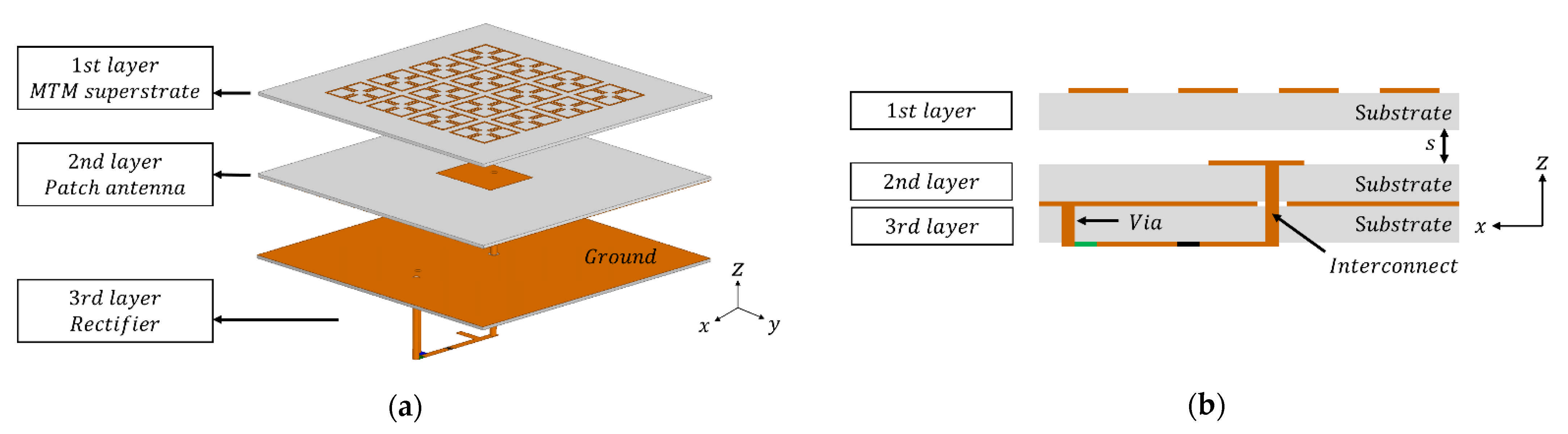
2. Design and Analysis of the MTM Integrated High-Gain Rectenna

The schematic of the MTM integrated high-gain rectenna is presented in Figure 2. As shown in Figure 2a, the MTM-integrated rectenna consists of 1st layer of the MTM superstrate, 2nd layer of the patch antenna, and 3rd layer of the rectifier circuit. The MTM superstrate is stacked on the patch antenna with the separation s. The rectifier circuit is connected to the coaxial feeding point of the patch antenna through the interconnect.

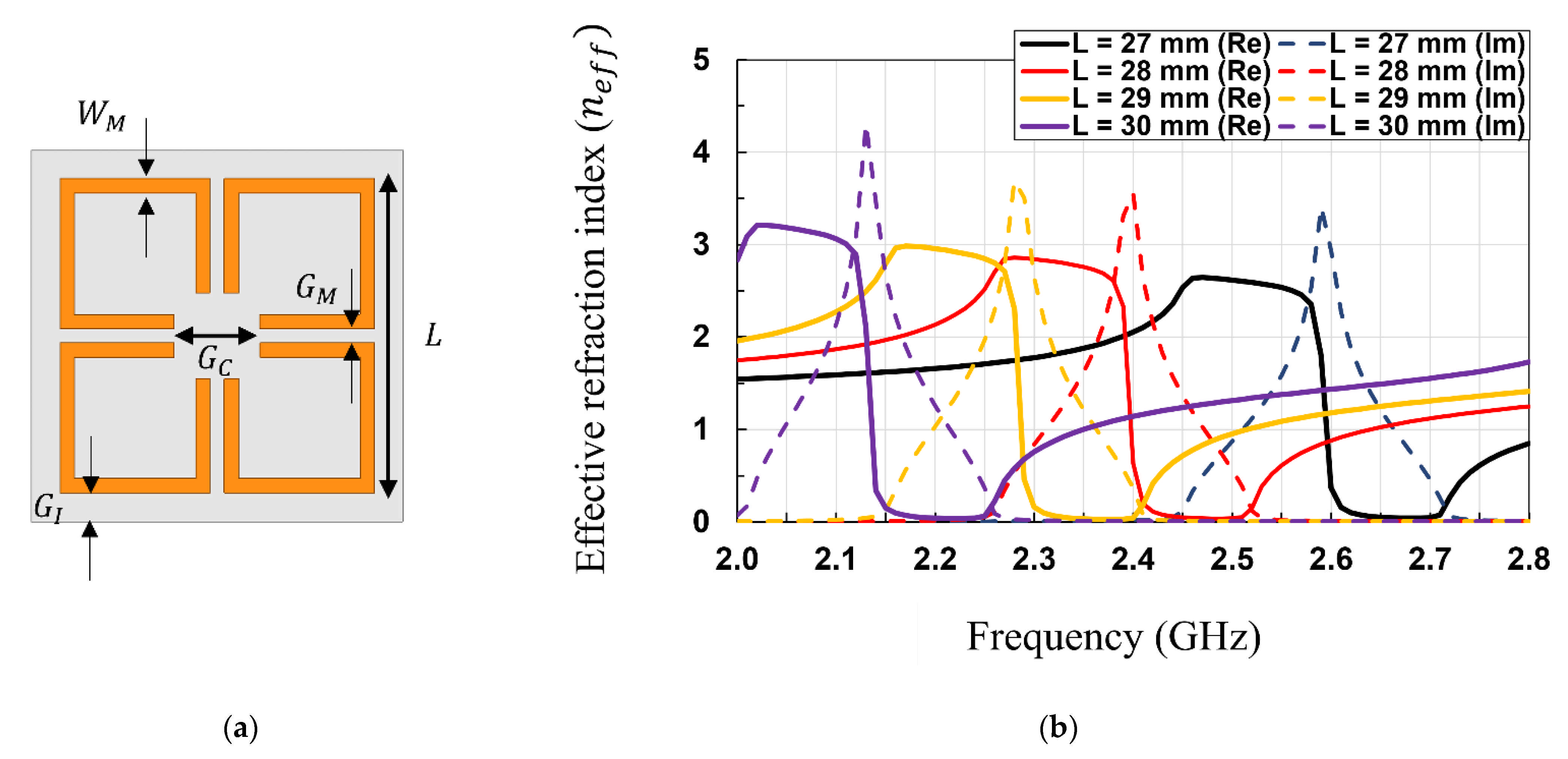
2.1. Design of the MTM Unit Cell

In this subsection, the MTM unit cell is designed to have the gain improvement property. In this work, a 4-leaf clover shaped MTM unit cell [21] is carefully designed to have a near-zero refractive index for 2.45 GHz, a popular industry, science, and medicine (ISM) band, where multiple applications such as Wi-Fi, Bluetooth, and ZigBee are used and its RF waves are abundant around us, and the unit cell is designed on an RO5880 substrate (ε = 2.2, δ = 0.0009) instead of FR4 (ε = 4.4, δ = 0.03) in order to minimize the substrate loss. To design the MTM unit cell that has the near-zero refractive index at 2.45 GHz, a parametric analysis is performed using High Frequency Structure Simulator (HFSS, Ansys Inc. Canonsburg, PA, USA). In the parametric analysis, the effective refractive index can be obtained from the simulation results by using the standard retrieval methods [26,27,28].
z = ± 1 + S 11 2 S 21 2 1 S 11 2 S 21 2      
e i n k 0 d = S 21 1 S 11 z 1 z + 1
n e f f = 1 k 0 d { [ ln e i n k 0 d ] + 2 m π i [ ln e i n k 0 d ] }
where S11 and S21 are the reflection and transmission coefficients; and denote the real part and imaginary part of the complex numbers, respectively; n e f f is the effective refractive index;   k 0 is the wavenumber;   d is the maximum thickness of the slab; z is the impedance; and m is the integer related to the branch index of n .
Figure 3a shows the schematic of the 4-leaf clover shaped MTM unit cell, and Figure 3b shows the simulated effective refraction index of the MTM unit cell with the varied L values while keeping other variables same for simplicity. In this analysis, the near-zero range is defined as the range where the real values of the effective refractive index are equal to or less than 0.5 ( η e f f r e 0.5 ) [25]. As shown in Figure 3b, the value of L is varied from 27 to 30 mm. When L increases, the near-zero range shifts to low frequencies, as depicted in Figure 3b. The L value is determined to be 28 mm, since the near-zero range of the MTM unit cell should be designed to include 2.45 GHz. As a result, the optimized near-zero range is shown to be from 2.4 to 2.54 GHz, which means the designed MTM changes the direction of the EM field by the boundary conditions to near-zero, thereby improving the gain of the antenna at the frequencies within this range.

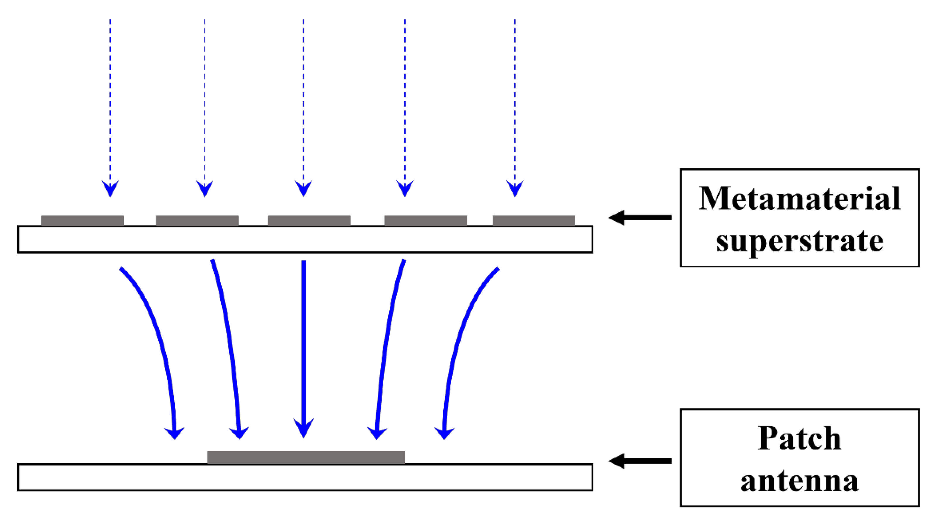
2.2. Design of the MTM Integrated Patch Antenna

In this subsection, the MTM integrated patch antenna is designed and simulated to verify the gain improvement property of the MTM superstrate. As shown in Figure 1, the MTM superstrate is stacked on the patch antenna. Firstly, the 2nd layer of the patch antenna is designed to be 47.8 mm × 39.9 mm for 2.45 GHz. Then, the MTM superstrate is placed over the patch antenna with a separation of 10 mm. In order to optimize the number of the MTM unit cells, the effects of the number of MTM unit cells on the performance of the integrated rectenna are investigated. We compare the radiation patterns of the patch antenna with a 2 × 2, 3 × 3, 4 × 4, and 5 × 5 MTM arrayed superstrate and without an MTM superstrate.
As shown in Figure 4, the gain of the patch antenna with a 4 × 4 MTM superstrate shows the highest peak gain, followed by the peak gain of the patch with a 5 × 5 MTM superstrate, and that with a 3 × 3 MTM superstrate, and that with a 2 × 2 MTM superstrate, and that without an MTM superstrate. The simulated peak gains of the patch antenna without and with an MTM superstrate are summarized in Table 1. As the number of the MTM unit cells increases, the peak gain tends to increase except for the case of the patch with the 5 × 5 MTM superstrate. Interestingly, the peak gain of the patch with the 5 × 5 MTM superstrate is slightly inferior to that with the 4 × 4 MTM superstrate. When the number of MTM unit cells in the array increases to 5 × 5, we expected the EM beam focusing coverage to be extended. However, since the beam focusing coverage of the 4 × 4 MTM superstrate is already enough to cover the size of the patch antenna, the peak gain improvement with the 5 × 5 MTM superstrate could be minute. Moreover, the simulation result indicates that the 5 × 5 MTM superstrate has increased loss compared with the 4 × 4 MTM superstrate, thereby decreasing the resultant peak gain of the antenna. Based on this analysis, it is concluded that the optimized number of the MTM unit cell in the array for the MTM superstrate is 4 × 4. Furthermore, it is worth noting that the number of MTM units could be determined depending on applications.

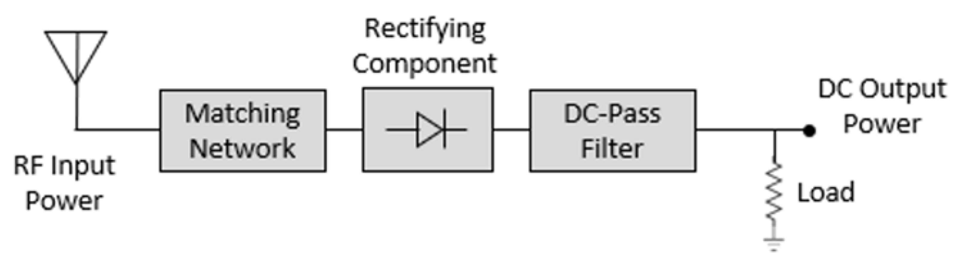
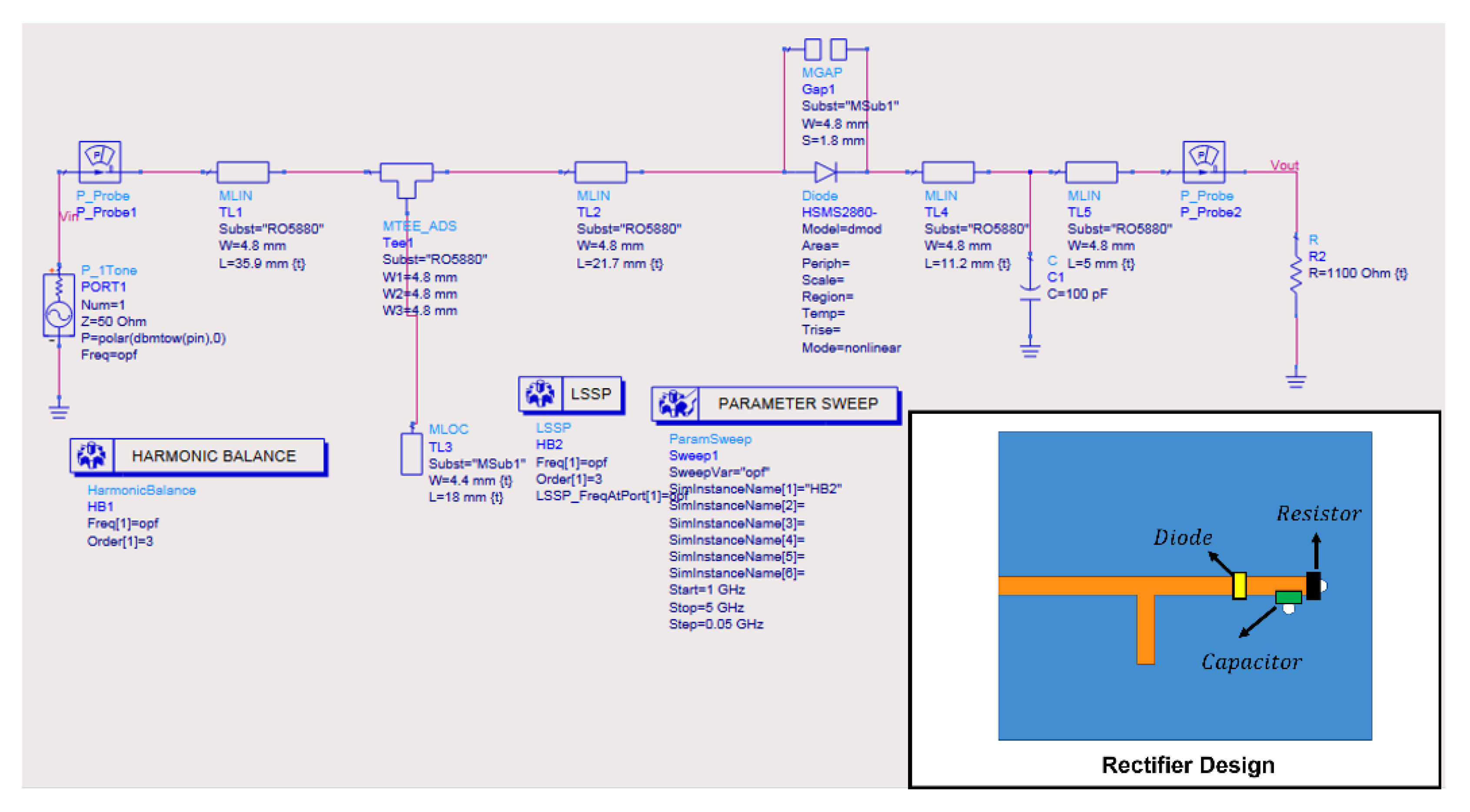
2.3. Design of the Rectifier Circuit

Figure 5 shows the block diagram of the rectifier circuit. A designed half-wave rectifier includes the matching circuit, rectifying component, DC-pass filter, and load. In this work, the rectifier is designed to have maximum RF–DC conversion efficiency at an input power of 10 dBm in order to provide sufficient output power to the end IoT devices. For the performance of the rectifier circuit, we utilize an HSMS2860 Schottky diode, which has a maximum forward voltage of 0.35 V. The rectifier circuit also contains a low-pass filter (100 pF shunt capacitor) and a resistive load (1.1k ohms). The choice of the capacitor and resistor values needs to fulfil a number of requirements. Firstly, the values must be chosen considering its cut-off frequency as its time constant should be very much longer than the time interval between the successive peaks of the rectified waveform. The value of the capacitor does not significantly affect the RF–DC conversion efficiency as long as the aforementioned criteria is satisfied. However, as for the value of the resistor, the optimum load resistor varies with frequency and input power. Here, the value of the load resistor and capacitor are optimized in Advanced Design System (ADS) software under an input power of 10 dBm to maximize the RF–DC conversion efficiency at 2.45 GHz. By sweeping the load resistance from 0.5 to 5 k ohms and the capacitance from 50 to 200 pF during the circuit optimization, the optimal values are found to be 1.1 k ohms for a resistor and 100 pF for a capacitor so that the conversion efficiency is the highest. The calculated cut-off frequency of the low-pass filter using selected values of the capacitor and resistor becomes 1.45 MHz, which can block high frequency band effectively. In addition, in order to ensure the maximal power transfer to the diode, a matching circuit is carefully designed at the diode input port. The impedance matching circuit is a crucial and also difficult part of the rectifier design. Due to the nonlinearity of the rectifier, the input impedance of the rectifier varies with the frequency, input power level, etc. In this work, an open stub is utilized to match the input impedance at 2.45 GHz at an input power of 10 dBm. The rectifier circuit is matched to 50 ohms since the input impedance of the MTM integrated antenna is 50 ohms.
As shown in Figure 6, ADS has been utilized for the simulation of the rectifier circuit. In order to consider the nonlinearity of the Schottky diode, Harmonic Balance simulation was utilized. In addition, the HSMS2860 spice model was utilized to obtain accurate simulation results. The detailed simulation results of the rectifier circuit are further discussed with the measurement results in Section 4.

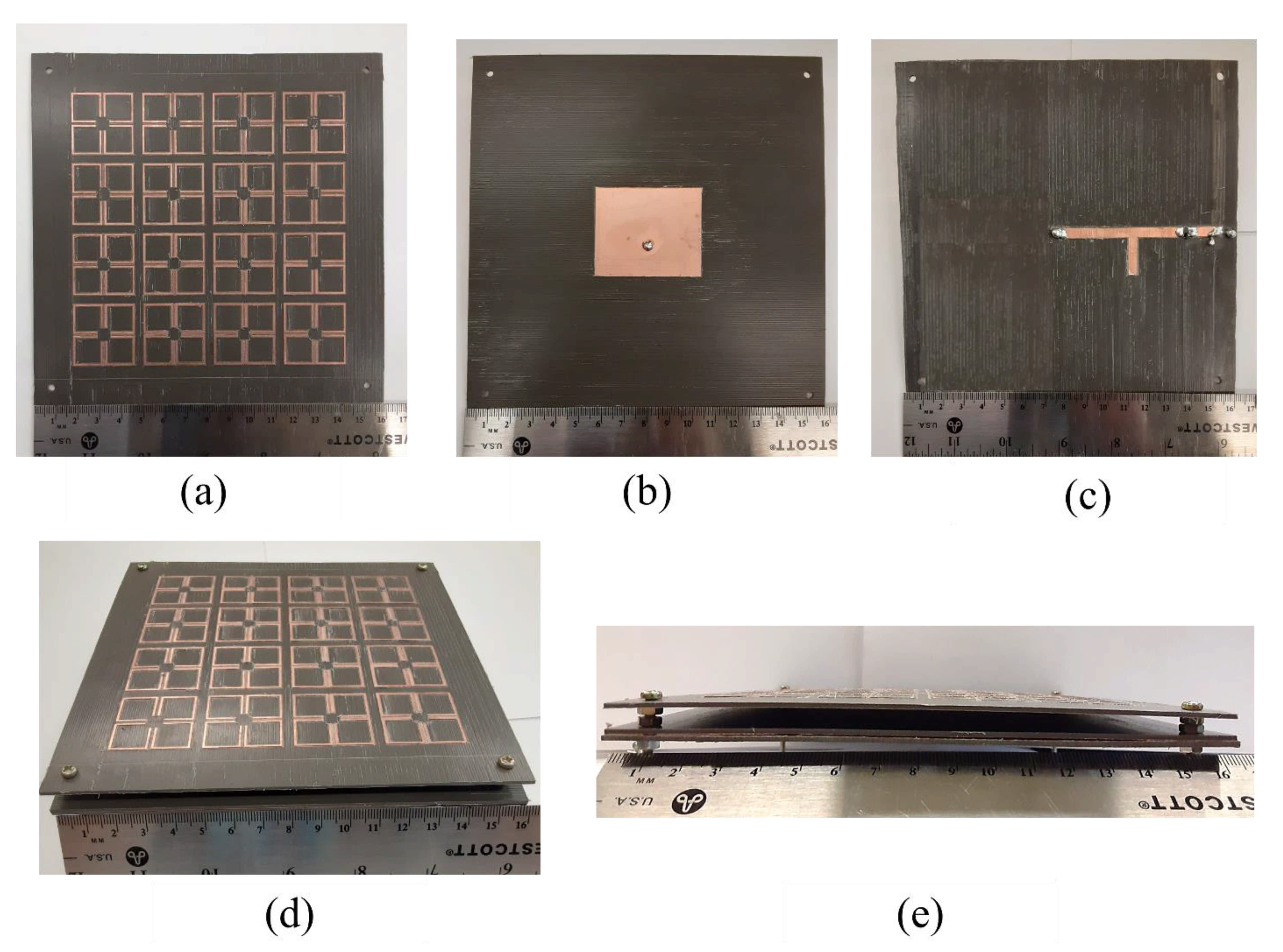
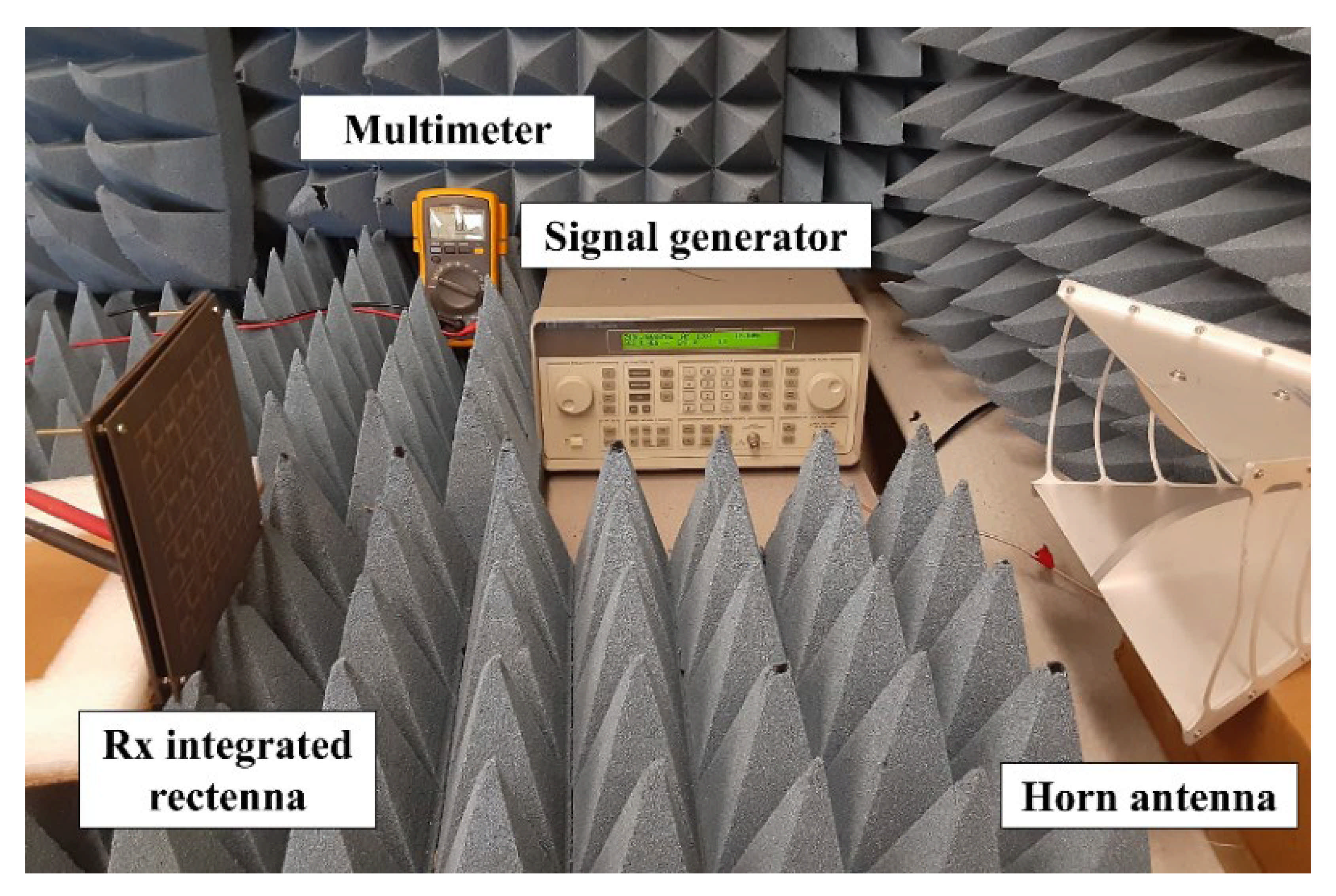
3. Fabrication of the MTM Integrated High-Gain Rectenna

The prototype of the MTM integrated high-gain rectenna is fabricated on an RO5880 substrate. Each layer of the MTM-integrated rectenna is fabricated using a milling machine. Figure 7a–c shows the fabricated MTM superstrate, patch antenna, and rectifier circuit. Then, the patch antenna is fully integrated with the MTM superstrate and rectifier circuit, as shown in Figure 7d,e. For the fabrication of the rectifier circuit, The Schottky diode (HSMS 2860, Avago Technologies Inc. San Jose, CA, USA), 1.1k ohms resistor (ERA-6AEB112V, Panasonic Electronics Inc. Kadoma, Osaka, Japan), and 100 pF capacitor (GCM1885G2A101FA16D, Murata Electronics Inc. Nagokakyo, Kyoto, Japan) are selected.

4. Simulated and Measured Results

In this section, we evaluate the performances of the MTM integrated high-gain rectenna and compare the measured results with the simulation results.

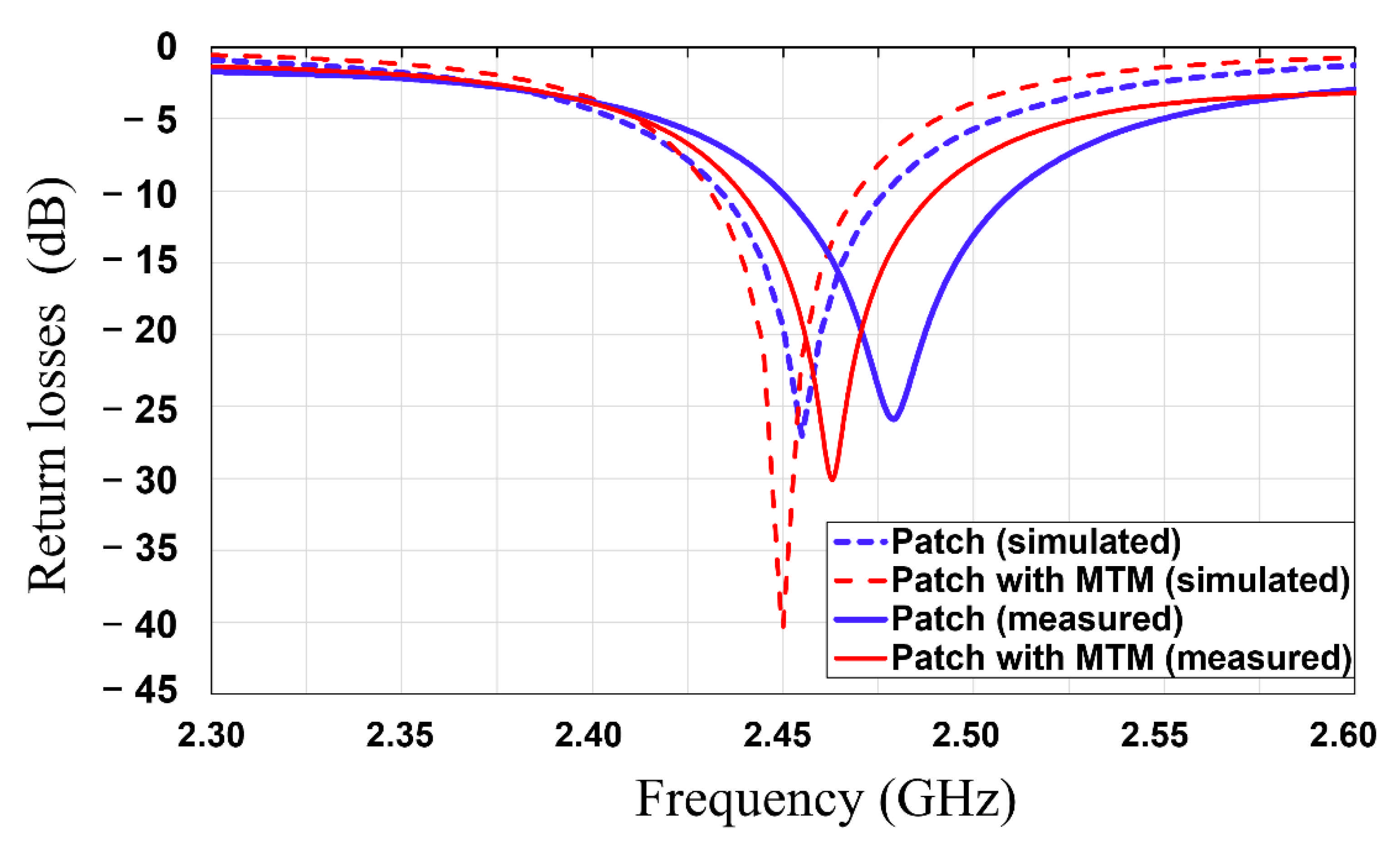
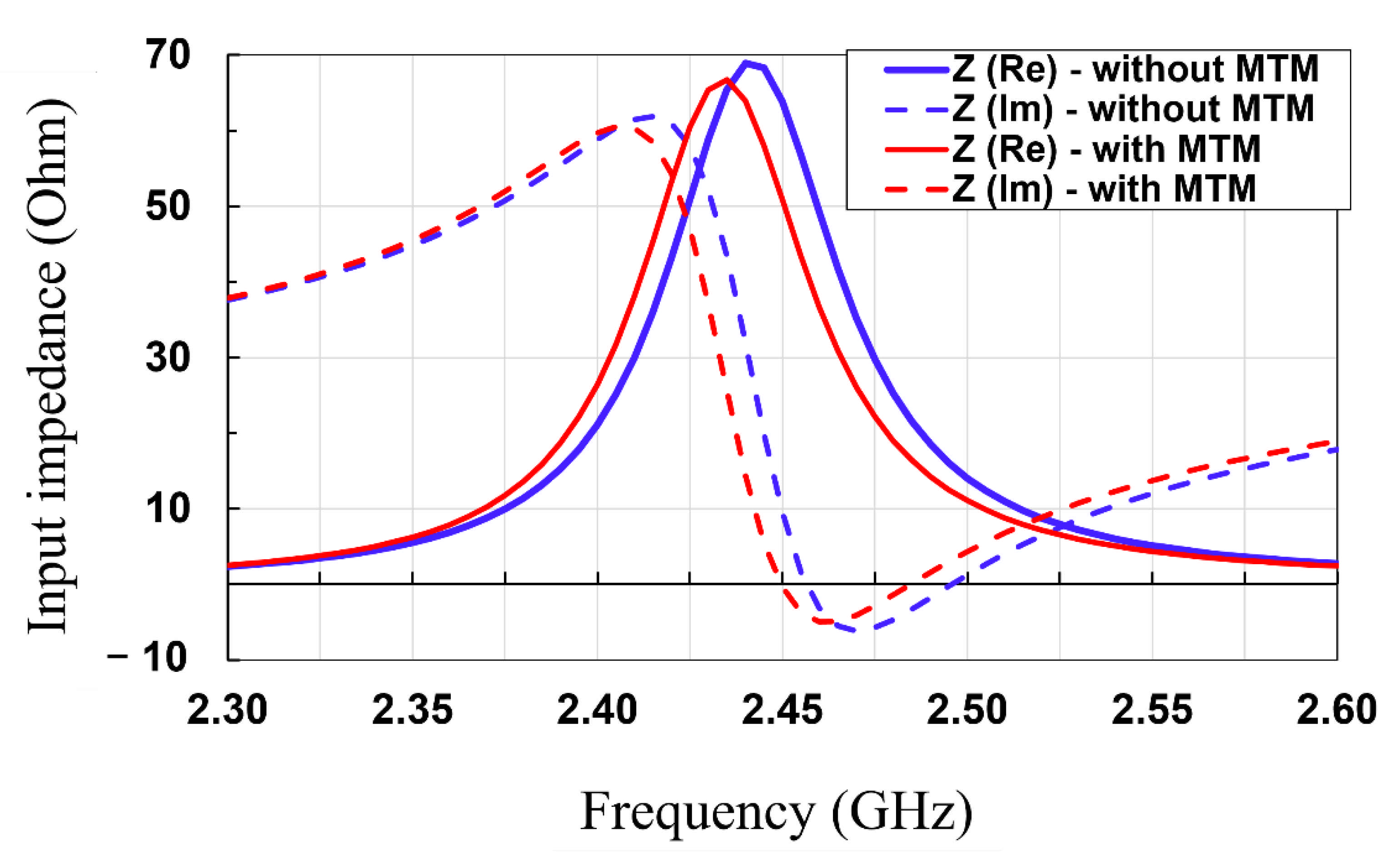
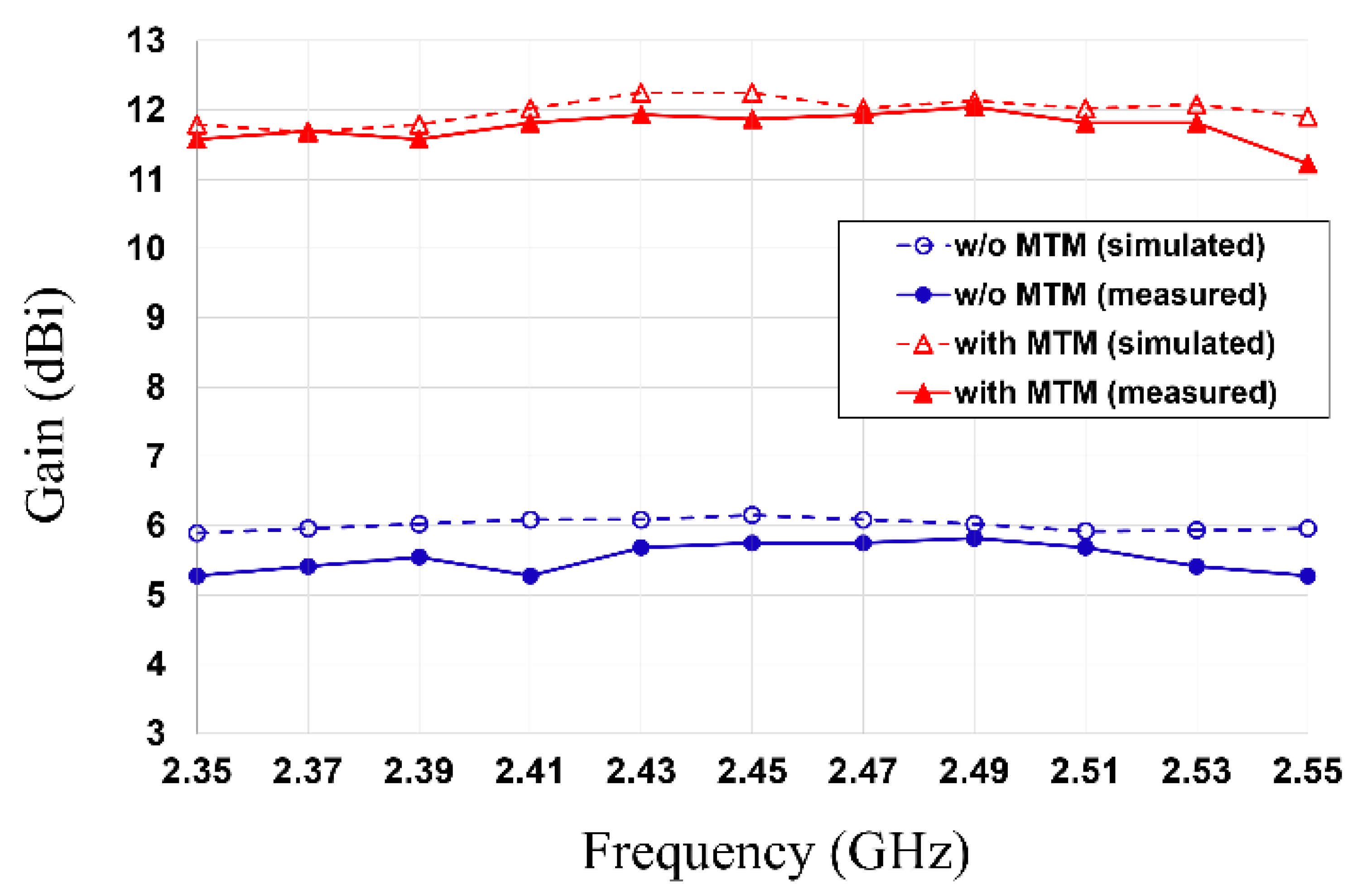
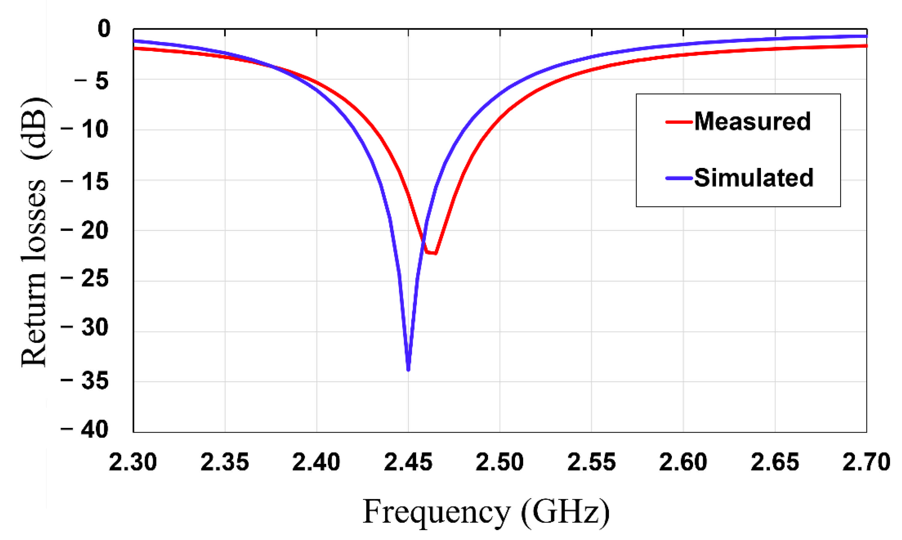
4.1. Simulated and Measured Results of the Patch Antenna with and without MTM Superstrate

In this subsection, the patch antenna with and without an MTM superstrate are simulated and measured, and their characteristics are compared. The return loss and peak gain of the antennas were measured using a vector network analyzer (HP E8361A, Agilent, Inc. Santa Clara, CA, USA) after standard one port short-open-load (SOL) calibration between 2.3 GHz and 2.6 GHz. Figure 8 shows the measured and simulated return losses of the patch with and without a 4 × 4 MTM superstrate. It is shown that the measured results are matched well with the simulated results. The measured resonant frequencies are a bit upshifted compared with the simulated ones, which are attributed to fabrication tolerance, i.e., the dimension of the fabricated devices is decreased during milling machine fabrication. In addition, the input impedances of the patch antenna with and without the MTM superstrate are simulated, as shown in the Figure 9. It is shown that, without MTM superstrate, the input resistance lies in the vicinity of 50 ohms with input reactance approximately near-zero at 2.46 GHz. With the MTM superstrate, the input resistance is shifted closer to ideal value of 50 ohms, and input reactance crossed zero at 2.45 GHz. Thus, the resonant frequency of the patch with the MTM superstrate is a bit downshifted compared with the one of the patch without MTM superstrate.
In addition, Figure 10 exhibits the simulated and measured peak gain of the antenna without and with an MTM superstrate as a function of frequency. The measured peak gain of the patch antenna is greatly enhanced from 5.75 dBi to 11.87 dBi (6.12 dB improvement) when the MTM superstrate is integrated on top of the patch. It means that the patch antenna architecture with an MTM superstrate can transfer 4.09 times as much power as the patch antenna without an MTM superstrate. The simulated and measured results in this section prove that the implemented MTM superstrate can serve as the beam-focusing lens, and the MTM superstrate is very effective for enhancing the antenna gain. The measured and simulated return loss and peak gain results are summarized in Table 2.

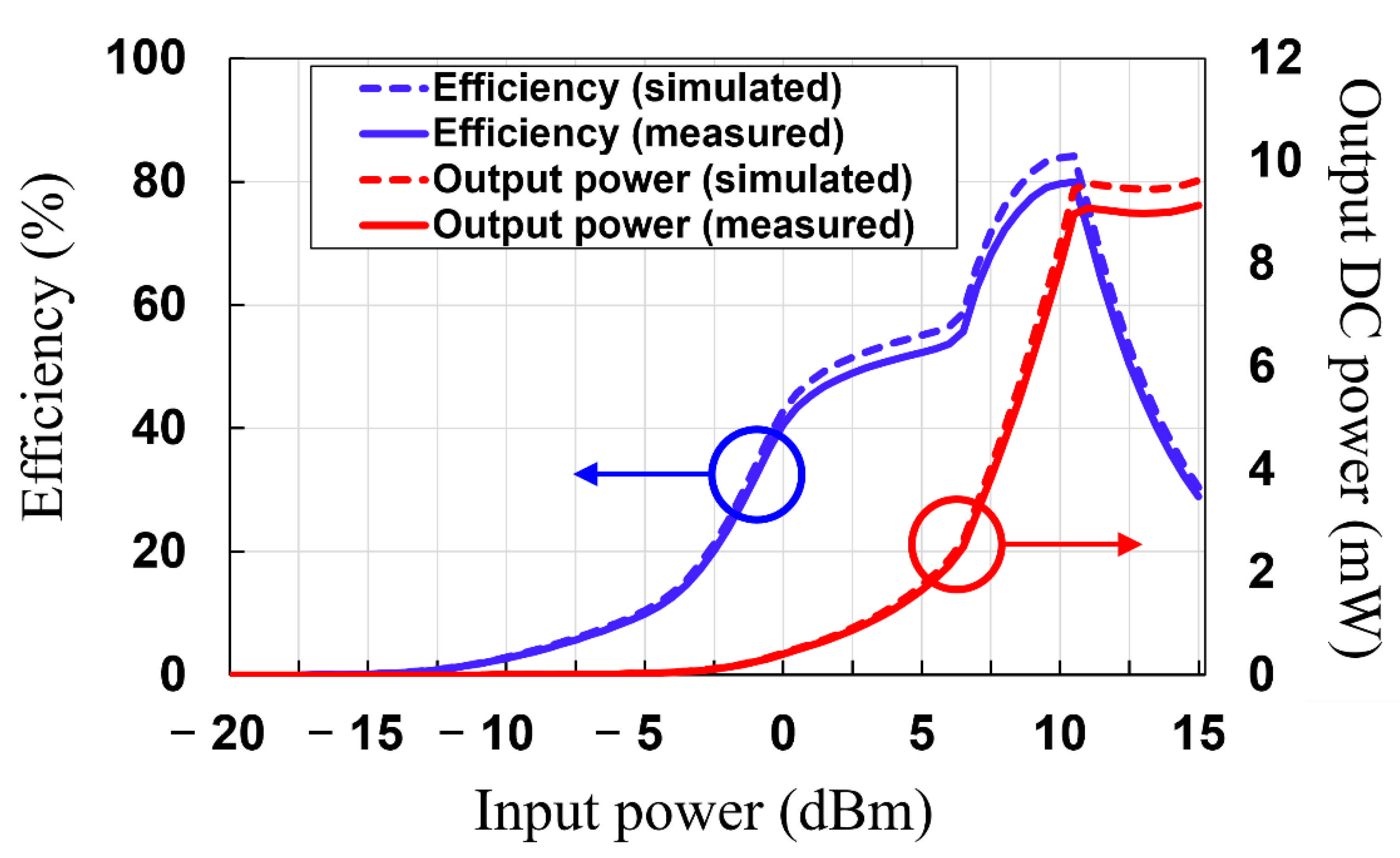
4.2. Simulated and Measured Results of the Rectifier Circuit

In this subsection, the third layer of the rectifier circuit is simulated, measured, and characterized. The ADS software was utilized for the simulation of the rectifier circuit. The measurement was performed using a vector network analyzer (HP E8361A, Agilent, Inc. Santa Clara, CA, USA), RF signal generator (HP 8648D, Agilent Inc. Santa Clara, CA, USA), and multimeter (Fluke 189). Firstly, the return loss of the rectifier circuit was simulated and measured using a vector network analyzer. Figure 11 shows that the measured results of the rectifier circuit exhibit a return loss of 22.4 dB at 2.47 GHz, which matches well with the simulated return loss of 33.6 dB at 2.45 GHz, which means the matching network of the rectifier matches well with the antenna.
Then, the RF–DC conversion efficiency of the rectifier circuit was simulated and measured. The RF–DC conversion efficiency of the rectifier can be obtained using the following Equation (4):
η R F dc = P o u t P i n × 100   % = V D C 2 P i n R L × 100   % ,
where P o u t is the output DC power, P i n is the input RF power to the rectifier circuit, R L is the load resistance value, and V D C is the output DC voltage. The simulated and measured RF–DC conversion efficiency and output DC power as a function of the input RF power levels to the rectifier circuit are depicted in Figure 12. The measured RF–DC conversion efficiencies are shown to be 2.69%, 40.71%, and 79.7% at −10 dBm, 0 dBm, and 10 dBm, respectively. A maximum RF–DC conversion efficiency of 79.96% is obtained at an input power of 10.5 dBm. The differences between simulated and measured results in Figure 10 can be attributed to: (1) The insertion loss of the SMA connector, which is connected between the RF signal generator and the rectifier circuit. This loss has not been taken into account in the ADS simulation. (2) The tolerance of the spice simulation model provided by the vendor of HSMS 2860 Schottky diode.

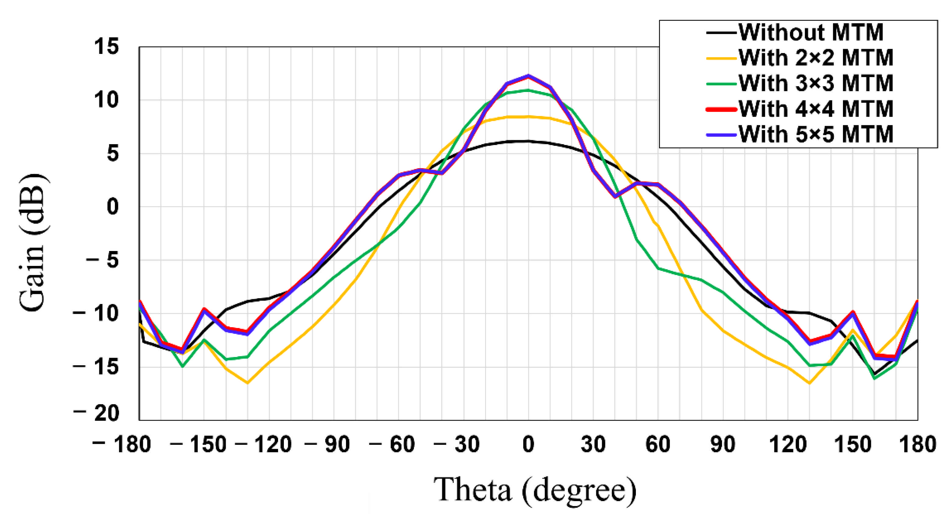
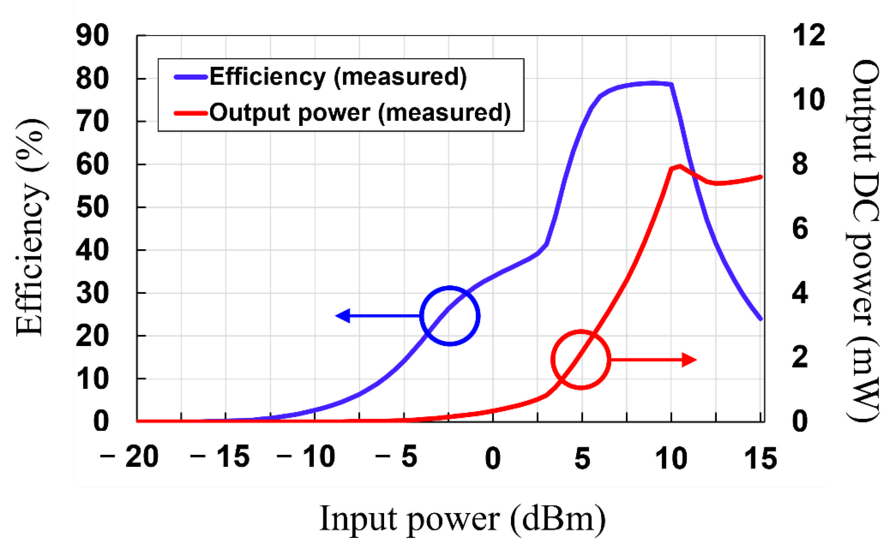
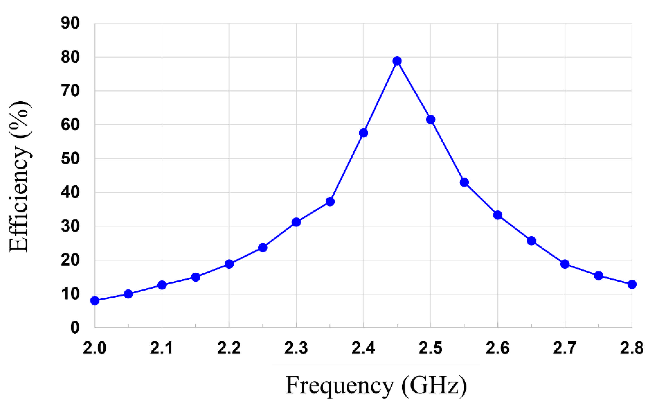
4.3. Measured Results of the MTM Integrated High-Gain Rectenna

Finally, the MTM integrated high-gain rectenna is fully integrated. Figure 13 shows the measurement setup of the MTM-integrated rectenna which consists of the RF signal generator, Tx horn antenna (JXTXLB-10180, A-INFO Inc. Irvine, CA, USA), Rx MTM-integrated rectenna, and multimeter. In the measurement, the MTM-integrated rectenna is placed at a distance of 40 cm away from the Tx antenna which satisfies the far-field condition at 2.45 GHz ( R 2 D 2 λ = 26.8   cm , where D is the largest dimension of the aperture of the antenna and λ is the free-space wavelength at the operating frequency). The RF–DC conversion efficiency of the rectenna can be calculated by:
η r e c t e n n a = V L 2 P r R L × 100   %
where P r is the RF power captured by the Rx integrated rectenna, R L is load resistance value, and V L is output voltage on the load. The RF power captured by the Rx integrated rectenna, P r , can be calculated by the Friis transmission equation:
P r = λ 4 π r 2 G t G r P t
where λ is the free-space wavelength at the operating frequency,   r is the distance between Tx and Rx rectenna, G t and G r is the gain of the Tx and Rx antenna, respectively, and P t is the Tx power. In the measurement, the values of G t and G r are 11 dB and 11.87 dB, respectively.
As shown in Figure 14, the measured RF–DC conversion efficiency and output DC power of the MTM-integrated rectenna as a function of the RF input power can be achieved using the aforementioned analysis. It is shown that the measured RF–DC conversion efficiency of 2.67%, 33.84%, and 78.63 is obtained at −10 dBm, 0 dBm, and 10 dBm, respectively, with the maximum RF–DC conversion efficiency of 78.9% being at an input power of 9 dBm. When the input power of the rectenna without MTM is 2.88 dBm, the input power can be increased to 9 dBm by integrating MTM. This results in the improvement of the RF–DC efficiency from 39.2% to 78.9% and the increase of the output DC power from 0.7 mW to 6.27 mW (a factor of 8.96 improvements). Moreover, the RF–DC conversion efficiency versus the frequency at an input power of 10 dBm is plotted in Figure 15. It is shown that the measured RF–DC conversion efficiency is higher than 50% in the range of 2.38 to 2.53 GHz.

4.4. Comparison

In this subsection, the MTM integrated high-gain rectenna is compared with previously reported high-gain rectennas. Firstly, the demonstrated MTM-integrated rectenna is compared with the preliminary study [25] in Table 3. The MTM-integrated rectenna shows overall improved performance in terms of peak gain, improved gain, and RF–DC conversion efficiency, which are attributed to the decreased substrate loss. The peak gains without/with MTM are improved by 0.97 dB and 1.17 dB, respectively. This enhancement can be interpreted as the substrate loss difference between FR4 and RO 5880. Furthermore, the demonstrated MTM-integrated rectenna shows improved RF–DC conversion efficiency compared with [25], which is also due to the reduced substrate loss of RO5880.
The demonstrated MTM-integrated rectenna is compared with the previously reported high-gain rectennas. Comparison parameters include the operating frequency; a technique that is used for the rectenna design; diode; antenna dimensions; RF input power/density (Pin/S); RF–DC conversion efficiency; design complexity/rectenna integration; and antenna gain. As shown in Table 4, the demonstrated MTM-integrated rectenna has shown outstanding performance compared to previously reported work. It is especially worth emphasizing that this is the first rectenna system utilizing the MTM superstrate integrated with the patch antenna and rectifier in a single device. Furthermore, the demonstrated work shows comparably high antenna gain and RF–DC conversion efficiency among selected work. Although the rectenna system demonstrated in [17] shows the highest gain, the rectenna exhibits a low RF–DC conversion efficiency of 42%, which leads to low end-to-end efficiency. In addition, the demonstrated MTM-integrated rectenna has a low design complexity compared with other work, as the MTM superstrate layer is integrated on top of the simple patch antenna and rectifier circuit.

5. Conclusions

In this work, the MTM integrated high-gain rectenna is demonstrated. The novel MTM superstrate approach with a three-layered integration method is firstly introduced for rectenna applications. The optimized near-zero property of the MTM unit cell is obtained using a parametric analysis. In addition, the effects of the number of MTM unit cells on the performance of the integrated rectenna are studied. By integrating the MTM on top of the patch antenna, the gain of the antenna is enhanced by 6.12 dB, resulting in the increase of incident RF power at the rectifier input, thereby inducing high-output DC power and high end-to-end efficiency. A measured RF–DC conversion efficiency of 2.67%, 33.84%, and 78.63 is achieved at −10 dBm, 0 dBm, and 10 dBm, respectively. A maximum RF–DC conversion efficiency of 78.9% is obtained at an input power of 9 dBm. When the input power of the rectenna without MTM is 2.88 dBm, the input power can be increased to 9 dBm by integrating MTM. This results in the improvement of the RF–DC efficiency from 39.2% to 78.9% and the increase of the output DC power from 0.7 mW to 6.27 mW (a factor of 8.96 improvements). The demonstrated MTM-integrated rectenna has shown outstanding performance compared to previously reported other work. It is especially worth emphasizing that this is the first rectenna system utilizing the MTM superstrate integrated with the patch antenna and rectifier in a single device. The demonstrated MTM-integrated rectenna has a low design complexity compared with other work, as the MTM superstrate layer is integrated on top of the simple patch antenna and rectifier circuit. In addition, the number of MTM units can be determined depending on applications. It is highly envisioned that the demonstrated MTM-integrated rectenna will provide new possibilities for practical energy harvesting applications with improved antenna gain and efficiency in various IoT environments.

Author Contributions

W.L.: conceptualization, software, methodology, data curation, validation, and writing—original draft preparation; S.-i.C.: data curation, validation, and writing—review and editing; H.-i.K.: software, and writing—review and editing; S.H.: data curation and visualization; S.J.: data curation and visualization; Y.-K.Y.: supervision, conceptualization, writing—review and editing, project administration, and funding acquisition. All authors have read and agreed to the published version of the manuscript.

Funding

This research was supported in part by ‘Beyond Limit Academia Collaboration Program’ funded by Samsung Electronics.

Institutional Review Board Statement

Not applicable.

Informed Consent Statement

Not applicable.

Data Availability Statement

Not applicable.

Acknowledgments

W. Lee is a recipient of the fellowship program by the Republic of Korea Army Headquarters. RF experiment/characterization was performed at the University of Florida.

Conflicts of Interest

The authors declare no conflict of interest.

References

  1. Arrawatia, M.; Baghini, M.S.; Kumar, G. Broadband bent triangular omnidirectional antenna for RF energy harvesting. IEEE Antennas Wirel. Propag. Lett. 2016, 15, 36–39. [Google Scholar] [CrossRef]
  2. Zakaria, Z.; Zainuddin, N.A.; Aziz, M.Z.A.A.; Husain, M.N.; Mutalib, M.A. Dual-band monopole antenna for energy harvesting system. In Proceedings of the IEEE Symposium on Wireless Technology and Applications (ISWTA), Kuching, Malaysia, 22–25 September 2013; pp. 225–229. [Google Scholar]
  3. Lin, W.; Ziolkowski, R.W. Electrically small, single-substrate huygens dipole rectenna for ultracompact wireless power transfer applications. IEEE Trans. Antennas Propag. 2021, 69, 1130–1134. [Google Scholar] [CrossRef]
  4. Sun, Y.; Guo, X.; He, M.; Zhong, Z. Design of a high-efficiency 2.45-GHz rectenna for low-input-power energy harvesting. IEEE Antennas Wirel. Propag. Lett. 2012, 11, 929–932. [Google Scholar]
  5. Tu, W.H.; Hsu, S.H.; Chang, K. Compact 5.8-GHz rectenna using stepped-impedance dipole antenna. IEEE Antennas Wirel. Propag. Lett. 2017, 6, 282–284. [Google Scholar] [CrossRef]
  6. Harouni, Z.; Cirio, L.; Osman, L.; Gharsallah, A.; Picon, O. A dual circularly polarized 2.45-GHz rectenna for wireless power transmission. IEEE Antennas Wirel. Propag. Lett. 2021, 10, 306–309. [Google Scholar] [CrossRef]
  7. Song, C.; Huang, Y.; Zhou, J.; Zhang, J.; Yuan, S.; Carter, P. A high-efficiency broadband rectenna for ambient wireless energy harvesting. IEEE Trans. Antennas Propag. 2015, 63, 3486–3495. [Google Scholar] [CrossRef] [Green Version]
  8. Song, C.; Huang, Y.; Carter, P.; Zhou, J.; Yuan, S.; Xu, Q.; Kod, M. A novel six-band dual CP rectenna using improved impedance matching technique for ambient RF energy harvesting. IEEE Trans. Antennas Propag. 2016, 64, 3160–3171. [Google Scholar] [CrossRef] [Green Version]
  9. Hassan, N.; Zakaria, Z.; Sam, W.Y.; Hanapiah, I.N.M.; Mohamad, A.N.; Roslan, A.F.; Ahmad, B.H.; Ismail, M.K.; Aziz, M.Z.A.A. Design of dual-band microstrip patch antenna with rightangle triangular aperture slot for energy transfer application. Int. J. RF Microw. Comput.-Aided Eng. 2019, 29, e21666. [Google Scholar] [CrossRef] [Green Version]
  10. Shi, Y.; Fan, Y.; Li, Y.; Yang, L.; Wang, M. An efficient broadband slotted rectenna for wireless power transfer at LTE band. IEEE Trans. Antennas Propag. 2019, 67, 814–822. [Google Scholar] [CrossRef]
  11. Hagerty, J.A.; Helmbrecht, F.B.; McCalpin, W.H.; Zane, R. Popovic, Z.B. Recycling ambient microwave energy with broad-band rectenna arrays. IEEE Trans. Microw. Theory Tech. 2004, 52, 1014–1024. [Google Scholar] [CrossRef]
  12. Strassner, B.; Chang, K. 5.8-GHz circularly polarized rectifying antenna for wireless microwave power transmission. IEEE Trans. Microw. Theory Tech. 2002, 50, 1870–1876. [Google Scholar] [CrossRef]
  13. Arrawatia, M.; Baghini, M.S.; Kumar, G. Differential microstrip antenna for RF energy harvesting. IEEE Trans. Antennas Propag. 2015, 63, 1581–1588. [Google Scholar] [CrossRef]
  14. Sun, H. An enhanced rectenna using differentially-fed rectifier for wireless power transmission. IEEE Antennas Wirel. Propag. Lett. 2016, 15, 32–35. [Google Scholar] [CrossRef]
  15. Ren, Y.J.; Chang, K. 5.8 GHz circularly polarized dual-diode rectenna and rectenna array for microwave power transmission. IEEE Trans. Microw. Theory Tech. 2006, 54, 1495–1502. [Google Scholar]
  16. Fakharian, M.M. A wideband rectenna using high gain fractal planar monopole antenna array for rf energy scavenging. Int. J. Antennas Propag. 2020, 2020, 3489323. [Google Scholar] [CrossRef]
  17. Ladan, S.; Guntupalli, A.B.; Wu, K. A high-efficiency 24 GHz rectenna development towards millimeter-wave energy harvesting and wireless power transmission. IEEE Trans. Circuits Syst. I Regul. Pap. 2014, 61, 3358–3366. [Google Scholar] [CrossRef]
  18. Yang, X.X.; Jiang, C.; Elsherbeni, A.Z.; Yang, F.; Wang, Y. A novel compact printed rectenna for data communication systems. IEEE Trans. Antennas Propag. 2013, 61, 2532–2539. [Google Scholar] [CrossRef]
  19. Samantaray, D.; Bhattacharyya, S. A Gain-Enhanced Slotted Patch Antenna Using Metasurface as Superstrate Configuration. IEEE Trans. Antennas Propag. 2020, 68, 6548–6556. [Google Scholar] [CrossRef]
  20. Singh, A.K.; Abegaonkar, M.P.; Koul, S.K. High-gain and high-aperture-efficiency cavity resonator antenna using metamaterial superstrate. IEEE Antennas Wirel. Propag. Lett. 2017, 16, 2388–2391. [Google Scholar] [CrossRef]
  21. Kim, C.; Lee, K.; Lee, S.; Kim, K.T.; Yoon, Y. A surface micromachined high directivity GPS patch antenna with a four-leaf clover shape metamaterial slab. In Proceedings of the 2012 IEEE 62nd Electronic Components and Technology Conference (ECTC), San Diego, CA, USA, 29 May–1 June 2012; pp. 942–947. [Google Scholar]
  22. Lee, W.; Kim, H.; Yoon, Y.-K. Metamaterial-inspired dual-function loop antenna for wireless power transfer and wireless communications. In Proceedings of the 2020 IEEE 70th Electronic Components and Technology Conference (ECTC), Orlando, FL, USA, 3–30 June 2020; pp. 1351–1357. [Google Scholar]
  23. Padilla, W.J.; Basov, D.N.; Smith, D.R. Negative refractive index metamaterials. Mater. Today 2006, 9, 28–35. [Google Scholar] [CrossRef]
  24. Lee, W.; Yoon, Y.-K. Wireless power transfer systems using metamaterials: A review. IEEE Access 2020, 8, 147930–147947. [Google Scholar] [CrossRef]
  25. Lee, W.; Kim, H.; Hwang, S.; Jeon, S.; Cho, H.; Yoon, Y.-K. 3D integrated high gain rectenna in package with metamaterial superstrates for high efficiency wireless power transfer applications. In Proceedings of the 2021 IEEE 71st Electronic Components and Technology Conference (ECTC), Virtual Meeting, 1 June–4 July 2021; pp. 1317–1322. [Google Scholar]
  26. Smith, D.; Schultz, S.; Markos, P.; Soukoulis, C. Determination of effective permittivity and permeability of metamaterials from reflection and transmission coefficients. Phys. Rev. B 2002, 65, 195104. [Google Scholar] [CrossRef] [Green Version]
  27. Smith, D.; Vier, D.; Koschny, T.; Soukoulis, C. Electromagnetic parameter retrieval from inhomogeneous metamaterials. Phys. Rev. E 2005, 71, 036617. [Google Scholar] [CrossRef] [Green Version]
  28. Chen, X.; Grzegorczyk, T.M.; Wu, B.-I.; Pacheco, J., Jr.; Kong, J.A. Robust method to retrieve the constitutive effective parameters of metamaterials. Phys. Rev. E 2004, 70, 016608. [Google Scholar] [CrossRef] [Green Version]
Figure 1. Principle of a gain improvement property of the MTM superstrate.
Sensors 21 06580 g001
Figure 2. Schematic of a 3D integrated rectenna: (a) perspective view, (b) side view, where s = 10   mm .
Sensors 21 06580 g002
Figure 3. (a) Schematic of the 4-leaf clover shaped MTM unit cell; (b) Simulated effective refraction index of the MTM unit cell with the varied L values ( L = 28   mm ,   W M = 1   mm ,   G M = 1   mm ,   G C = 6   mm ,   G I = 2   mm ).
Sensors 21 06580 g003
Figure 4. Simulated radiation patterns of the patch antenna with and without an MTM superstrate.
Sensors 21 06580 g004
Figure 5. Block diagram of the rectifier circuit.
Sensors 21 06580 g005
Figure 6. ADS schematic of the rectifier circuit.
Sensors 21 06580 g006
Figure 7. (a) Fabricated MTM superstrate, (b) fabricated patch antenna, (c) fabricated rectifier, (d) fabricated MTM-integrated rectenna, (e) side view of the fabricated MTM-integrated rectenna.
Sensors 21 06580 g007
Figure 8. Simulated and measured return loss results of the patch antenna without and with MTM superstrate.
Sensors 21 06580 g008
Figure 9. Simulated input impedance of the patch antenna without and with MTM superstrate.
Sensors 21 06580 g009
Figure 10. Simulated and measured peak gain of the patch antenna with and without MTM superstrate.
Sensors 21 06580 g010
Figure 11. Simulated and measured return loss results of the rectifier circuit.
Sensors 21 06580 g011
Figure 12. Simulated and measured return loss results of the rectifier circuit.
Sensors 21 06580 g012
Figure 13. Measurement setup for the MTM-integrated rectenna.
Sensors 21 06580 g013
Figure 14. Measured RF–DC conversion efficiency of the MTM-integrated rectenna.
Sensors 21 06580 g014
Figure 15. Measured RF–DC conversion efficiency versus frequency of the MTM-integrated rectenna.
Sensors 21 06580 g015
Table 1. Simulated peak gains of the patch antenna without and with an MTM superstrate.
CasePeak Gain
(dBi)
Improved Peak Gain (dB)
Patch only6.15-
Patch with 2 × 2 MTM superstrate8.442.29
Patch with 3 × 3 MTM superstrate10.934.78
Patch with 4 × 4 MTM superstrate12.36.15
Patch with 5 × 5 MTM superstrate12.256.1
Table 2. Simulated and measured performances of the patch antenna with and without MTM superstrate.
ParametersPatch OnlyPatch with MTM
SimulatedMeasuredSimulatedMeasured
Return loss (dB)−27.05−25.88−40.34−30.13
Resonant frequency (GHz)2.462.4792.452.465
10-dB bandwidth (GHz)0.0390.0440.0510.061
Peak gain (dBi)6.155.7512.311.87
Table 3. Comparison of This Work with Preliminary Work.
Parameters[25]This Work
SubstrateFR4
(ε = 4.4, δ = 0.03)
RO5880
(ε = 2.2, δ = 0.0009)
Operating Frequency2.45 GHz2.45 GHz
Dimensions (mm3)150 × 150 × 14.71
(0.18 λ3)
158 × 158 × 14.71
(0.199 λ3)
Peak gain without MTM4.78 dBi5.75 dBi
Peak gain with MTM10.7 dBi11.87 dBi
Improved gain5.92 dB6.12 dB
Resistive load1 kΩ1.1 kΩ
Peak RF–DC conversion efficiency63.5%
@ 10.5 dBm input
78.9%
@ 9 dBm input
DC power at peak efficiency6.35 mW6.27 mW
Table 4. Comparison of This Work with Other High-Gain Rectennas.
Ref.Operating
Frequency
(GHz)
TechniqueDiodeAntenna
Dimensions
(mm3)
Pin (dBm)/
S (µW/cm2)
RF–DC Conversion Efficiency (%)Design
Complexity/Rectenna Integration
Antenna Gain
(dBi)
[12]5.8Reflecting surfaceMA40150-119-20/-80High/Yes10.7
[4]2.45Reflecting surfaceHSMS2852110 × 90 × 20.6 *
(0.113 λ3)
-/1.9580.03Low/Yes8.6
[13]0.9Differential patch-137 × 137 × 21.2
(0.01 λ3)
2.19/-65.3High/No8.5
[16]0.95Antenna arrayHSMS285C165 × 165 × 0.8
(0.18 λ3)
5/-76High/No8.5
[17]24SIW cavityMA4E131755 × 55 × 0.5 *
(0.776 λ3)
12.55/-42High/Yes12.6
[9]2.4Air gap,
aperture coupling
HSMS286B110 × 89 × 5.07
(0.026 λ3)
10/-32.52Intermediate/No7.82
[18]5.78Aperture couplingHSMS286040 × 40 × 1.6
(0.026 λ3)
13.98/-63High/No7
This work2.45MTM superstrateHSMS2560158 × 158 × 14.71 *
(0.199 λ3)
9/-78.9Low/Yes11.87
* Includes the rectifier dimension as the rectenna integrated in a single device.
Publisher’s Note: MDPI stays neutral with regard to jurisdictional claims in published maps and institutional affiliations.

