A Low-Resources TDC for Multi-Channel Direct ToF Readout Based on a 28-nm FPGA


Abstract
:1. Introduction
- Calibration technique
- The selection of the best S-C combination improves linearity. By searching for the most uniform configuration of the delay line, the linearity improves without time resolution degradation and additional dead time and resource usage.
- The online calibration resulted from a code density test, improving accuracy even further.
- Compactness
- The synchronization module consists of only two FFs, efficiently shaping any input pulse;
- The ones-zeros encoder requires low resource usage; it features a mere 8-ns propagation time. Moreover, it is robust against bubble errors, without requiring any additional correction logic.
- Reference frequency optimization for short TDL. It is adapted to the FPGA speed grade. With this approach, we can implement 400 TDC channels at 125 Msamples/s.
- Full electrical characterization
- We have provided full electrical characterization, including power consumption and resource usage estimation. These parameters are important in portable systems for distance ranging applications based on direct ToF, which requires multiple parallel channels.
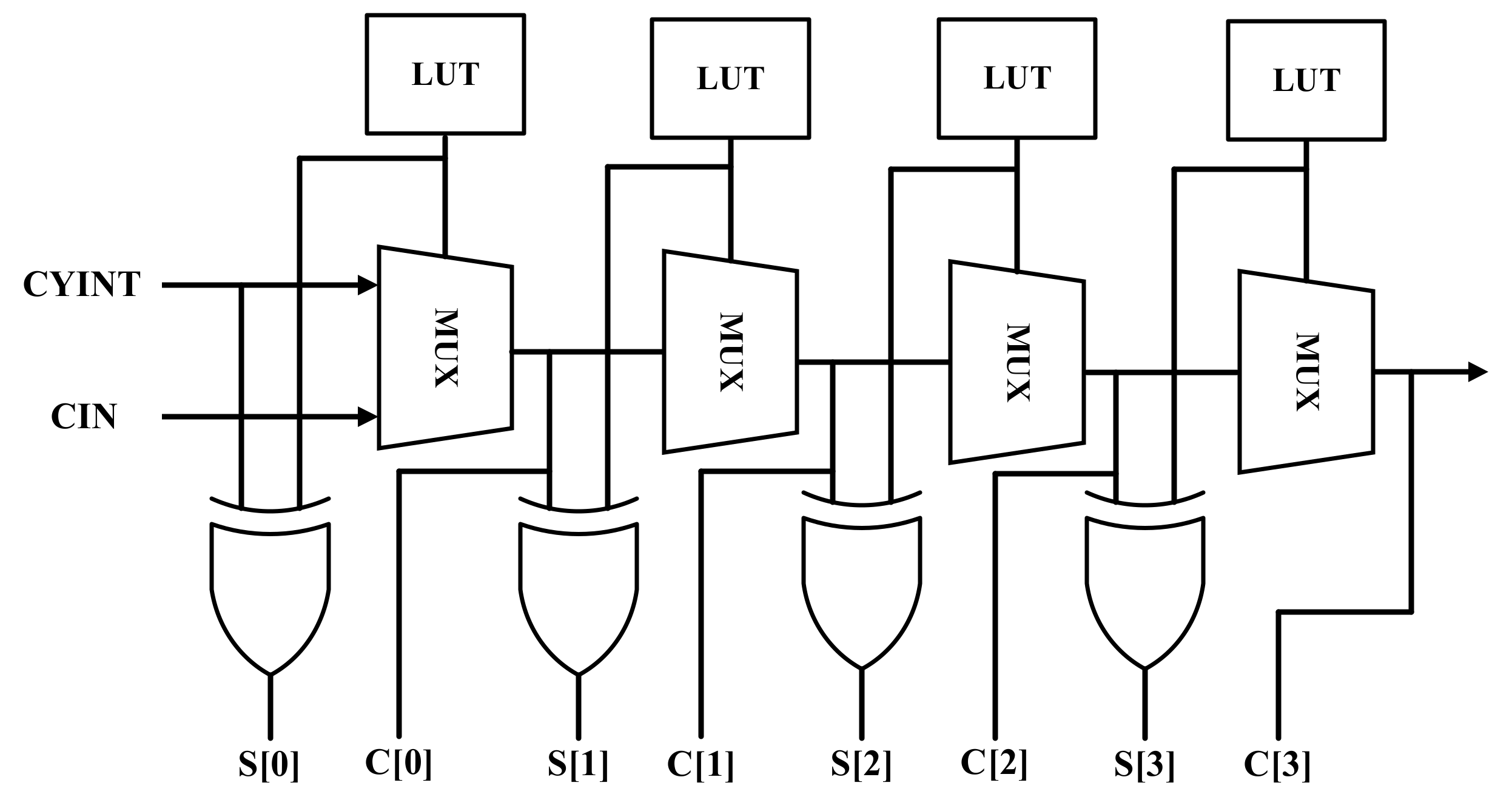
2. TDC Architecture
3. Experimental Results
3.1. Measurements
3.2. Comparison
4. Conclusions
Author Contributions
Funding
Data Availability Statement
Conflicts of Interest
References
- Burri, S.; Bruschini, C.; Charbon, E. LinoSPAD: A Compact Linear SPAD Camera System with 64 FPGA-Based TDC Modules for Versatile 50 ps Resolution Time-Resolved Imaging. Instruments 2017, 1, 6. [Google Scholar] [CrossRef] [Green Version]
- Stoppa, D.; Pancheri, L.; Scandiuzzo, M.; Gonzo, L.; Betta, G.-F.D.; Simoni, A. A CMOS 3-D Imager Based on Single Photon Avalanche Diode. IEEE Trans. Circuits Syst. I Regul. Pap. 2007, 54, 4–12. [Google Scholar] [CrossRef]
- Vornicu, I.; Carmona-Galan, R.; Rodriguez-Vazquez, A. Arrayable Voltage-Controlled Ring-Oscillator for Direct Time-of-Flight Image Sensors. IEEE Trans. Circuits Syst. I Regul. Pap. 2017, 64, 2821–2834. [Google Scholar] [CrossRef]
- Gersbach, M.; Trimananda, R.; Maruyama, Y.; Fishburn, M.W.; Stoppa, D.; Richardson, J.; Walker, R.; Henderson, R.; Charbon, E. High frame-rate TCSPC-FLIM using a novel SPAD-based image sensor. SPIE-Intl. Soc. Optical Eng. 2010, 7780, 77801H. [Google Scholar]
- Veerappan, C.; Richardson, J.; Walker, R.; Li, D.D.-U.; Fishburn, M.W.; Maruyama, Y.; Stoppa, D.; Borghetti, F.; Gersbach, M.; Henderson, R.K.; et al. A 160 × 128 single-photon image sensor with on-pixel 55ps 10b time-to-digital converter. In Proceedings of the 2011 IEEE International Solid-State Circuits Conference, San Francisco, CA, USA, 20–24 February 2011; pp. 312–314. [Google Scholar]
- Spanoudaki, V.; Levin, C. Photo-detectors for time of flight positron emission tomography (ToF-PET). Sensors 2010, 10, 10484–10505. [Google Scholar] [CrossRef]
- Braga, L.H.C.; Gasparini, L.; Grant, L.; Henderson, R.K.; Massari, N.; Perenzoni, M.; Stoppa, D.; Walker, R. A Fully Digital 8×16 SiPM Array for PET Applications With Per-Pixel TDCs and Real-Time Energy Output. IEEE J. Solid-State Circuits 2013, 49, 301–314. [Google Scholar] [CrossRef]
- Zieliński, M.; Kowalski, M. Review of single-stage time-interval measurement modules implemented in FPGA devices. Metrol. Meas. Syst. 2009, 16, 641–647. [Google Scholar]
- Machado, R.; Cabral, J.; Alves, F.S. Recent Developments and Challenges in FPGA-Based Time-to-Digital Converters. IEEE Trans. Instrum. Meas. 2019, 68, 4205–4221. [Google Scholar] [CrossRef]
- Parsakordasiabi, M.; Vornicu, I.; Carmona-Galán, R.; Rodríguez-Vázquez, Á. A survey on FPGA-based high-resolution TDCs. In Proceedings of the 13th International Conference on Distributed Smart Cameras, Trento, Italy, 9–11 September 2019; Association for Computing Machinery (ACM): New York, NY, USA, 2019; p. 27. [Google Scholar]
- Song, J.; An, Q.; Liu, S. A high-resolution time-to-digital converter implemented in field-programmable-gate-arrays. IEEE Trans. Nucl. Sci. 2006, 53, 236–241. [Google Scholar] [CrossRef]
- Favi, C.; Charbon, E. A 17ps time-to-digital converter implemented in 65nm FPGA technology. In Proceedings of the ACM/SIGDA international symposium on Field programmable gate arrays—FPGA ’09, Monterey, CA, USA, 22–24 February 2009. [Google Scholar]
- Fishburn, M.; Menninga, L.H.; Favi, C.; Charbon, E. A 19.6 ps, FPGA-Based TDC With Multiple Channels for Open Source Applications. IEEE Trans. Nucl. Sci. 2013, 60, 2203–2208. [Google Scholar] [CrossRef]
- Szplet, R.; Kalisz, J.; Szymanowski, R. Interpolating time counter with 100 ps resolution on a single FPGA device. IEEE Trans. Instrum. Meas. 2000, 49, 879–883. [Google Scholar] [CrossRef]
- Amiri, A.; Boukadoum, M.; Khouas, A. A Multihit Time-to-Digital Converter Architecture on FPGA. IEEE Trans. Instrum. Meas. 2008, 58, 530–540. [Google Scholar] [CrossRef]
- Balla, A.; Beretta, M.M.; Ciambrone, P.; Gatta, M.; Gonnella, F.; Iafolla, L.; Mascolo, M.; Messi, R.; Moricciani, D.; Riondino, D. The characterization and application of a low resource FPGA-based time to digital converter. Nucl. Instrum. Methods Phys. Res. Sect. A Accel. Spectrometers Detect. Assoc. Equip. 2014, 739, 75–82. [Google Scholar] [CrossRef]
- Büchele, M.; Fischer, H.; Gorzellik, M.; Herrmann, F.; Königsmann, K.; Schill, C.; Schopferer, S. A 128-channel Time-to-Digital Converter (TDC) inside a Virtex-5 FPGA on the GANDALF module. J. Instrum. 2012, 7, C03008. [Google Scholar] [CrossRef]
- Zhang, J.; Zhou, D. A new delay line loops shrinking time-to-digital converter in low-cost FPGA. Nucl. Instrum. Methods Phys. 2015, 771, 10–16. [Google Scholar] [CrossRef]
- Zhang, M.; Wang, H.; Liu, Y. A 7.4 ps FPGA-Based TDC with a 1024-Unit Measurement Matrix. Sensors 2017, 17, 865. [Google Scholar] [CrossRef] [PubMed] [Green Version]
- Wu, J.; Shi, Z. The 10-ps wave union TDC: Improving FPGA TDC resolution beyond its cell delay. In Proceedings of the 2008 IEEE Nuclear Science Symposium Conference Record, Dresden, Germany, 19–25 October 2008; pp. 3440–3446. [Google Scholar]
- Liu, C.; Wang, Y. A 128-Channel, 710 M Samples/Second, and Less Than 10 ps RMS Resolution Time-to-Digital Converter Implemented in a Kintex-7 FPGA. IEEE Trans. Nucl. Sci. 2015, 62, 773–783. [Google Scholar] [CrossRef]
- Won, J.Y.; Kwon, S.I.; Yoon, H.S.; Ko, G.B.; Son, J.-W.; Lee, J.S. Dual-Phase Tapped-Delay-Line Time-to-Digital Converter With On-the-Fly Calibration Implemented in 40 nm FPGA. IEEE Trans. Biomed. Circuits Syst. 2016, 10, 231–242. [Google Scholar] [CrossRef]
- Kuang, J.; Wang, Y.; Cao, Q.; Liu, C. Implementation of a high precision multi-measurement time-to-digital convertor on a Kintex-7 FPGA. Nucl. Instrum. Methods Phys. Res. Sect. A Accel. Spectrometers Detect. Assoc. Equip. 2018, 891, 37–41. [Google Scholar] [CrossRef]
- Won, J.Y.; Lee, J.S. Time-to-Digital Converter Using a Tuned-Delay Line Evaluated in 28-, 40-, and 45-nm FPGAs. IEEE Trans. Instrum. Meas. 2016, 65, 1678–1689. [Google Scholar] [CrossRef]
- Wu, J. Several Key Issues on Implementing Delay Line Based TDCs Using FPGAs. IEEE Trans. Nucl. Sci. 2010, 57, 1543–1548. [Google Scholar] [CrossRef]
- Wang, Y.; Liu, C. A 3.9 ps Time-Interval RMS Precision Time-to-Digital Converter Using a Dual-Sampling Method in an UltraScale FPGA. IEEE Trans. Nucl. Sci. 2016, 63, 2617–2621. [Google Scholar] [CrossRef]
- Hu, X.; Zhao, L.; Liu, S.; Wang, J.; An, Q. A stepped-up tree encoder for the 10-ps wave union TDC. IEEE Trans. Nucl. Sci. 2013, 60, 3544–3549. [Google Scholar] [CrossRef]
- Wang, Y.; Liu, C. A Nonlinearity Minimization-Oriented Resource-Saving Time-to-Digital Converter Implemented in a 28 nm Xilinx FPGA. IEEE Trans. Nucl. Sci. 2015, 62, 2003–2009. [Google Scholar] [CrossRef]
- Chen, H.; Li, D.D. Multichannel, Low Nonlinearity Time-to-Digital Converters Based on 20 and 28 nm FPGAs. IEEE Trans. Ind. Electron. 2019, 66, 3265–3274. [Google Scholar] [CrossRef] [Green Version]
- Wang, Y.; Kuang, J.; Liu, C.; Cao, Q. A 3.9 ps RMS Precision Time-to-Digital Converter Using Ones Counter Encoding Scheme in a Kintex-7 FPGA. IEEE Trans. Nucl. Sci. 2017, 64, 1. [Google Scholar] [CrossRef]
- Wu, J.; Shi, Z.; Wang, I. Firmware-only implementation of time-to-digital converter (TDC) in field-programmable gate array (FPGA). In Proceedings of the 2003 IEEE Nuclear Science Symposium. Conference Record (IEEE Cat. No.03CH37515), Portland, OR, USA, 19–25 October 2003; Volume 1, pp. 177–181. [Google Scholar]
- Wang, J.; Liu, S.; Shen, Q.; Li, H.; An, Q. A fully fledged TDC implemented in field-programmable gate arrays. IEEE Trans. Nucl. Sci. 2010, 57, 446–450. [Google Scholar] [CrossRef]
- Cova, S.; Bertolaccini, M. Differential linearity testing and precision calibration of multichannel time sorters. Nucl. Instrum. Methods 2002, 77, 269–276. [Google Scholar] [CrossRef]
- Arabul, E.; Girach, A.; Rarity, J.; Dahnoun, N. Precise multi-channel timing analysis system for multi-stop LIDAR correlation. In Proceedings of the 2017 IEEE International Conference on Imaging Systems and Techniques (IST), Beijing, China, 18–20 October 2017; pp. 1–6. [Google Scholar]
- Cao, G.; Xia, H.; Dong, N. An 18-ps TDC using timing adjustment and bin realignment methods in a Cyclone-IV FPGA. Rev. Sci. Instrum. 2018, 89, 054707. [Google Scholar] [CrossRef]
- Townsend, T.; Tang, Y.; Chen, J. Highly-linear FPGA-based Data Acquisition System for Multi-channel SiPM Readout. In Proceedings of the Topical Workshop on Electronics for Particle Physics—PoS(TWEPP2019), Santiago De Compostela, Spain, 2–6 September 2019; Sissa Medialab: Trieste, Italy, 2020; Volume 370, p. 094. [Google Scholar]
- Homulle, H.; Charbon, E. Basic FPGA TDC Design. 2015. Available online: http://cas.tudelft.nl/fpga_tdc/TDC_basic.html (accessed on 4 January 2021).
- Tontini, A.; Gasparini, L.; Pancheri, L.; Passerone, R. Design and characterization of a low-cost FPGA-based TDC. IEEE Trans. Nucl. Sci. 2018, 65, 680–690. [Google Scholar] [CrossRef]
- Kelly, O. XEM7310 User’s Manual. 3 March 2018. Available online: https://docs.opalkelly.com/display/XEM7310 (accessed on 4 January 2021).
- Kelly, O. Front Panel User’s Manual. Available online: http://assets00.opalkelly.com/library/FrontPanel-UM.pdf (accessed on 4 January 2021).
- Xilinx. Artix-7 FPGAs Data Sheet: DC and AC Switching Characteristics (DS181). 18 June 2018. Available online: https://www.xilinx.com/support/documentation/data_sheets/ds181_Artix_7_Data_Sheet.pdf (accessed on 4 January 2021).
- Xilinx. 7 Series FPGAs Clocking Resources (UG472). 30 July 2018. Available online: https://www.xilinx.com/support/documentation/user_guides/ug472_7Series_Clocking.pdf (accessed on 4 January 2021).
- Kim, K.; Kim, Y.; Yu, W.; Cho, S. A 7 bit, 3.75 ps Resolution Two-Step Time-to-Digital Converter in 65 nm CMOS Using Pulse-Train Time Amplifier. IEEE J. Solid-State Circuits 2013, 48, 1009–1017. [Google Scholar] [CrossRef]


| I/O | Resources | Processing Time | ||
|---|---|---|---|---|
| Input | Output | LUTs | FFs | |
| 192 codes | 8b | 215 | 246 | 6 clocks |
| Sampling Pattern | DNL (LSB) | INL (LSB) |
|---|---|---|
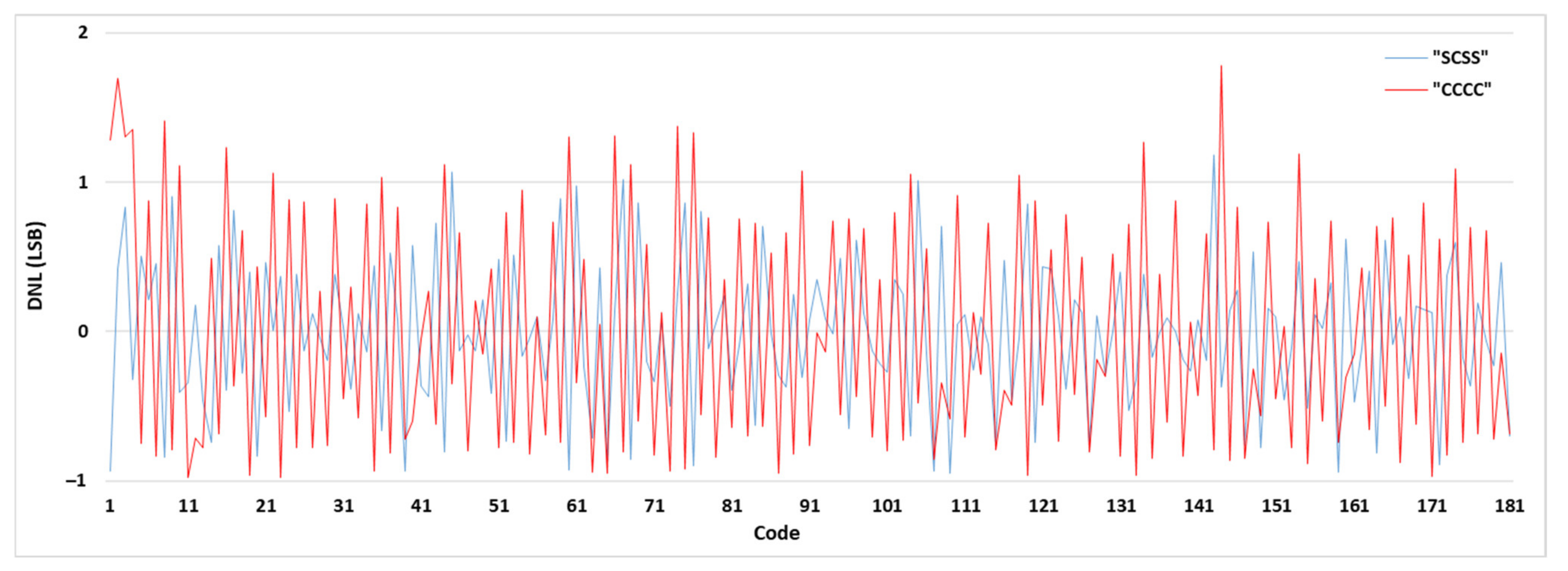
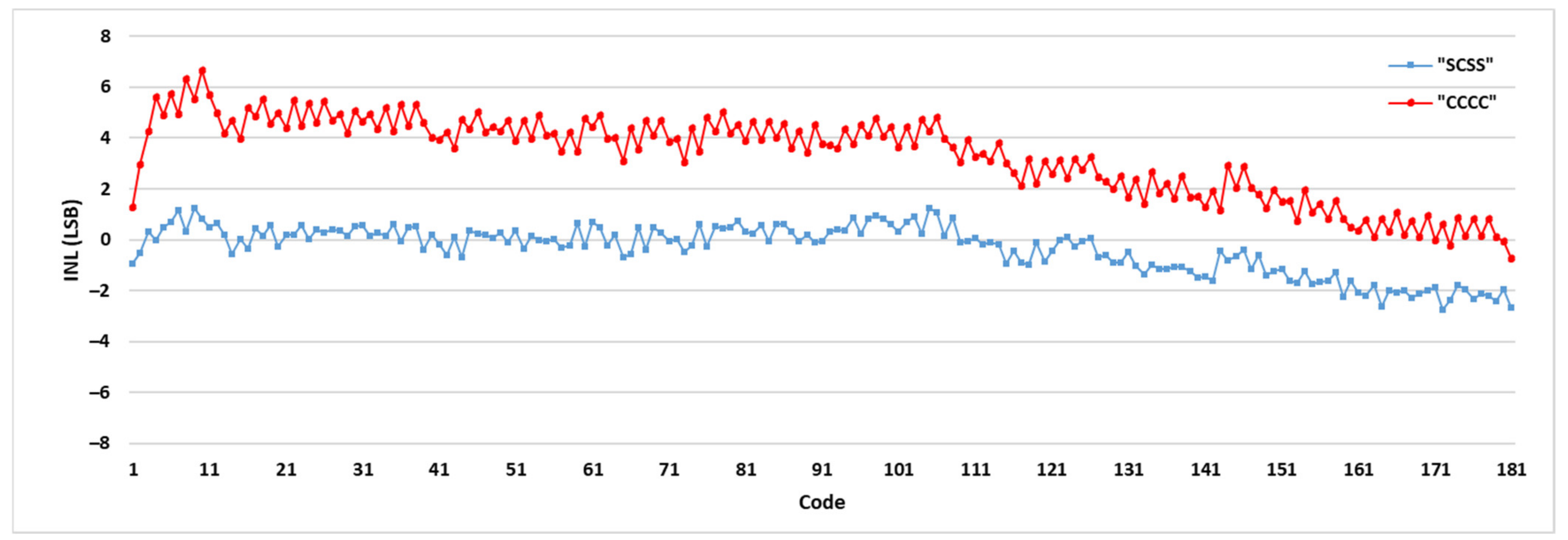
| CCCC | [−0.976, 1.779] | [−0.733, 6.660] |
| CSCS | [−0.987, 3.721] | [−0.733, 6.567] |
| SCSC | [−0.954, 1.425] | [−2.921, 1.274] |
| CCSC | [−0.978, 2.727] | [−0.119, 6.456] |
| CSCC | [−0.981, 3.698] | [−0.700, 6.700] |
| SCSS | [−0.953, 1.185] | [−2.750, 1.238] |
| Resource | Available | Utilization | Utilization (%) |
|---|---|---|---|
| LUT | 133,800 | 216 | 0.16 |
| FF | 267,600 | 638 | 0.24 |
| BRAM | 365 | 2.50 | 0.68 |
| Total Power Consumption | 164 mW | ||
| Dynamic Power | 33 mW | ||
| Parameter | Value/Range | Unit |
|---|---|---|
| Clock Frequency | 250 | MHz |
| Resolution | 22.2 | ps |
| Measurement Range | 262.14 | μs |
| Dead-Time | 8 | ns |
| Readout Speed | 125 | MSample/s |
| INL | [−0.953, 1.185] | LSB |
| DNL | [−2.750, 1.238] | LSB |
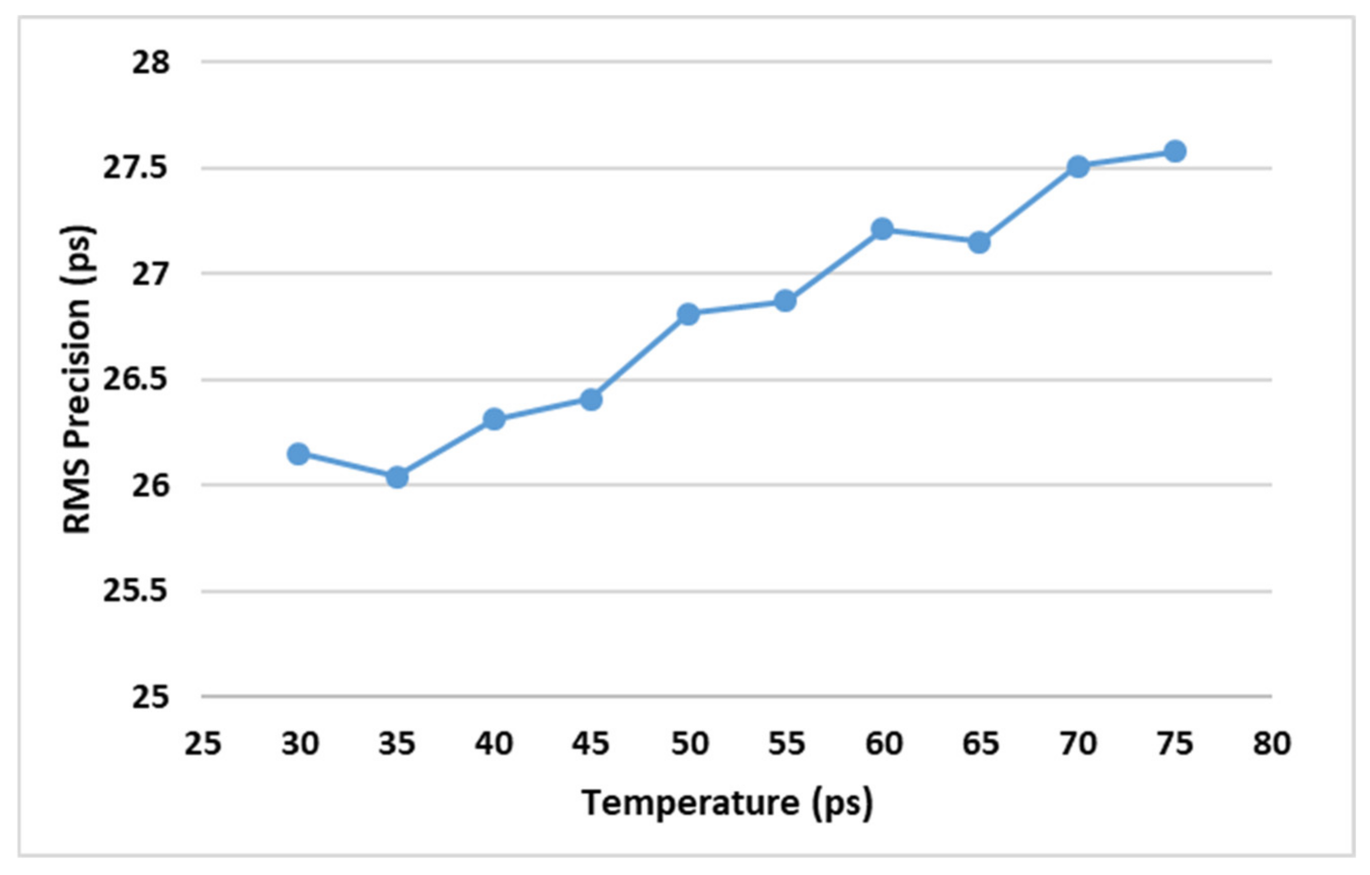
| Single-Shot Precision | 26.04 | ps |
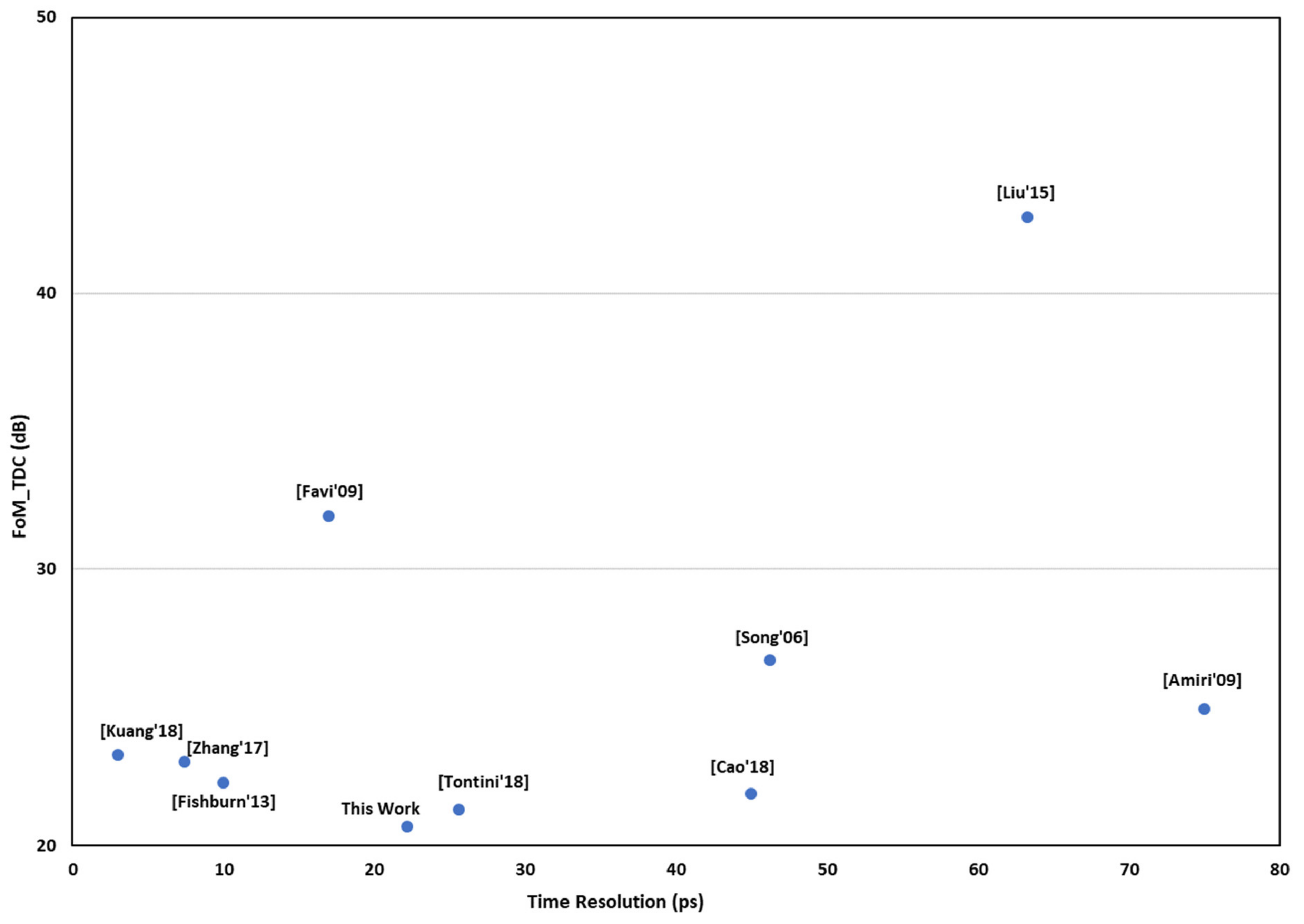
| Ref. | Used Method | FPGA | LSB [ps] | Precision [ps] | DNL [LSB] | INL [LSB] | Dead-Time [ns] | Resources Usage | Power [mW] | ENoB | FOM_TDC (dB) |
|---|---|---|---|---|---|---|---|---|---|---|---|
| Song [11] | TDL | Virtex-2 | 46.2 | 65.8 | 1.10 | 2 | 10 | NS | NS | 5.42 | 26.71 |
| Wu [20] | Wave Union | Cyclone II | 30 | 25 | NS | NS | 5 | NS | NS | NA | NA |
| Amiri [15] | Matrix of Vernier Delays | Spartan-3 | 75 | 300 | 2.5 | 3 | 4.17 | NS | 92 | 5 | 24.95 |
| Favi [12] | TDL | Virtex-5 | 17 | 24.2 | 3.55 | 3 | 50 | 1208 Slices | NS | 5 | 31.94 |
| Buchele [17] | Multi-phase Clock | Virtex-5 | 160 | 68 | 0.8 | NS | NS | NS | NS | NA | NA |
| Fishburn [13] | TDL | Virtex-6 | 10 | 19.6 | 1.5 | 2.25 | 3.3 | NS | NS | 5.30 | 22.29 |
| Zhang [18] | Delay Line Loops Shrinking | SmartFusion | 63.3 | 61.7 | 0.55 | 0.72 | 1410 | NS | NS | 6.22 | 42.77 |
| Liu [21] | Multi-Meas. TDL | Kintex-7 | 9.4 | 9.5 | 4.6 | NS | 1.47 | 400 Slices | NS | NA | NA |
| Wang [28] | TDL + Bin Realignment & Decimation | Kintex-7 | 17.6 | 15 | 1 | 0.8 | NS | NS | NS | 7.15 | NA |
| Won [22] | Dual-phase TDL + Online Cal. | Virtex-6 | 10 | 12.83 | 1.91 | 3.93 | NS | NS | NS | 5.70 | NA |
| Cao [35] | TDL + Bin Realignment | Cyclone-IV | 45 | 18 | 0.5 | 0.48 | 13.3 | NS | NS | 6.43 | 21.88 |
| Wang [30] | Mul-Ch. TDL + ones Counter Encoder | Kintex-7 | 2.45 | 3.9 | NS | NS | 3.61 | 6258 FFs + 2433 LUTs | 821 | NA | NA |
| Zhang [19] | Matrix of Counters | Virtex-5 | 7.4 | 6.8 | 0.74 | 1.57 | 80 | 1265 Slices | 1113 | 8.64 | 23.03 |
| Kuang [23] | Multi-Meas. RO-based TDL | Kintex-7 | 3 | 5.76 | NS | 9 | 22 | NS | NS | 6.68 | 23.27 |
| Chen [29] | sub-TDL + tap timing + histogram + mixed cal. | Virtex-7 | 10.54 | 14.59 | 0.08 | 0.11 | NS | 1916 FFs + 1145 LUTs | NS | 7.85 | NA |
| Tontini [38] | Input Stage + Tuned TDL | Spartan-6 | 25.6 | 37 | 1.23 | 2.96 | 8.69 | 415 Slices | 131 | 6.01 | 21.29 |
| This work | Input Stage+ Tuned TDL + Combinatory Encoder | Artix-7 | 22.2 | 26.04 | 1.18 | 2.75 | 8 | 638 FFs + 216 LUTs | 164 (Total) | 6.10 | 20.68 |
Publisher’s Note: MDPI stays neutral with regard to jurisdictional claims in published maps and institutional affiliations. |
© 2021 by the authors. Licensee MDPI, Basel, Switzerland. This article is an open access article distributed under the terms and conditions of the Creative Commons Attribution (CC BY) license (http://creativecommons.org/licenses/by/4.0/).
Share and Cite
Parsakordasiabi, M.; Vornicu, I.; Rodríguez-Vázquez, Á.; Carmona-Galán, R. A Low-Resources TDC for Multi-Channel Direct ToF Readout Based on a 28-nm FPGA. Sensors 2021, 21, 308. https://doi.org/10.3390/s21010308
Parsakordasiabi M, Vornicu I, Rodríguez-Vázquez Á, Carmona-Galán R. A Low-Resources TDC for Multi-Channel Direct ToF Readout Based on a 28-nm FPGA. Sensors. 2021; 21(1):308. https://doi.org/10.3390/s21010308
Chicago/Turabian StyleParsakordasiabi, Mojtaba, Ion Vornicu, Ángel Rodríguez-Vázquez, and Ricardo Carmona-Galán. 2021. "A Low-Resources TDC for Multi-Channel Direct ToF Readout Based on a 28-nm FPGA" Sensors 21, no. 1: 308. https://doi.org/10.3390/s21010308