Article

Fabrication and Characteristics of a Three-Axis Accelerometer with Double L-Shaped Beams

The Key Laboratory of Electronics Engineering, College of Heilongjiang Province, Heilongjiang University, Harbin 150080, China
*
Author to whom correspondence should be addressed.
Sensors 2020, 20(6), 1780; https://doi.org/10.3390/s20061780
Submission received: 17 February 2020 / Revised: 19 March 2020 / Accepted: 20 March 2020 / Published: 24 March 2020
(This article belongs to the Section Physical Sensors)

Abstract

:
A three-axis accelerometer with a double L-shaped beams structure was designed and fabricated in this paper, consisting of a supporting body, four double L-shaped beams and intermediate double beams connected to two mass blocks. When applying acceleration to the accelerometer chip, according to the output voltage changes of three Wheatstone bridges constituted by twelve piezoresistors on the roots of the beams, the corresponding acceleration along three axes can be measured based on the elastic force theory and piezoresistive effect. To improve the characteristics of the three-axis accelerometer, we simulated how the width of the intermediate double beams affected the characteristics. Through optimizing the structure size, six chips with different widths of intermediate double beams were fabricated on silicon-on-insulator (SOI) wafers using micro-electromechanical systems (MEMS) technology and were packaged on printed circuit boards (PCB) by using an electrostatic bonding process and inner lead bonding technology. At room temperature and VDD = 5.0 V, the resulting accelerometer with an optimized size (w = 500 μm) realized sensitivities of 0.302 mV/g, 0.235 mV/g and 0.347 mV/g along three axes, with a low cross-axis sensitivity. This result provides a new strategy to further improve the characteristics of the three-axis accelerometer.

1. Introduction

In recent years, with the rapid development of semiconductor technology, accelerometers have been widely used in many different fields, mainly including vibration detection [1], consumer electronics [2], medical treatment [3,4], vibration detection of wind turbines [5], navigation [6,7], automobile safety [8], and so on. Currently, although accelerometers have met the needs of real life, they are still facing the challenge of a wide measurement range, high accuracy, etc. Thus, high performance accelerometers have stimulated a particular attention from researchers, providing an opportunity to improve the characteristics of the accelerometer, making it possible to overcome the above mentioned limitation. For example, Sankar et al. proposed a quad beam silicon piezoresistive z-axis accelerometer with a very low cross-axis sensitivity of 0.316 μV/V∙g for an in-plane acceleration in 2013 [9]. After that, Han et al. presented a piezoresistive accelerometer with a low cross-axis sensitivity based on masked-maskless wet etching, realizing sensitivities of 0.069 V/V∙g, 0.034 V/V∙g and 4.15 V/V∙g along the x-axis, y-axis and z-axis, and cross-axis sensitivities of 1.67% and 0.82% along the x-axis and y-axis, respectively [10]. Recently, Takahashi et al. reported an angular acceleration sensor composed of liquid ring channels and piezoresistive cantilevers as the sensing element, achieving an angular acceleration resolution of 0.01 rad/s2 in the range of 0.1–100 Hz on a target axis about 100 times higher than that of the other axes, a high sensitivity and a low cross-interference [11]. Nowadays, the accelerometer can be divided into several types, mainly including piezoresistive, capacitive [12], piezoelectric [13], etc. The piezoresistive accelerometer, when compared with the ones having other structures, exhibits many excellent properties, such as a fast response, easy signal processing and miniaturization, etc. However, the piezoresistive accelerometers are also facing challenges with respect to improving measurement consistency and reducing cross-interference, which have limited their further development.
To overcome the above obstacles, a piezoresistive three-axis accelerometer with double L-shaped beams was designed and fabricated on a silicon-on-insulator (SOI) wafer using MEMS technology in this study. Using the double L-shaped beams concentrated the stress distribution under the actions of ax and ay. Through a simulation to investigate how the width of the intermediate double beams affects the characteristics of an accelerometer, the structure size of the intermediate double beams was optimized. The test results indicate that it is possible to achieve the measurement of acceleration along three axes and reduce the cross-axis sensitivity using the resulting accelerometer. The study on the effects of intermediate double beams’ structure sizes on the sensitivity of the proposed accelerometer provides a possibility to further improve the performance of three-axis accelerometers.

2. Basic Structure and Working Principle

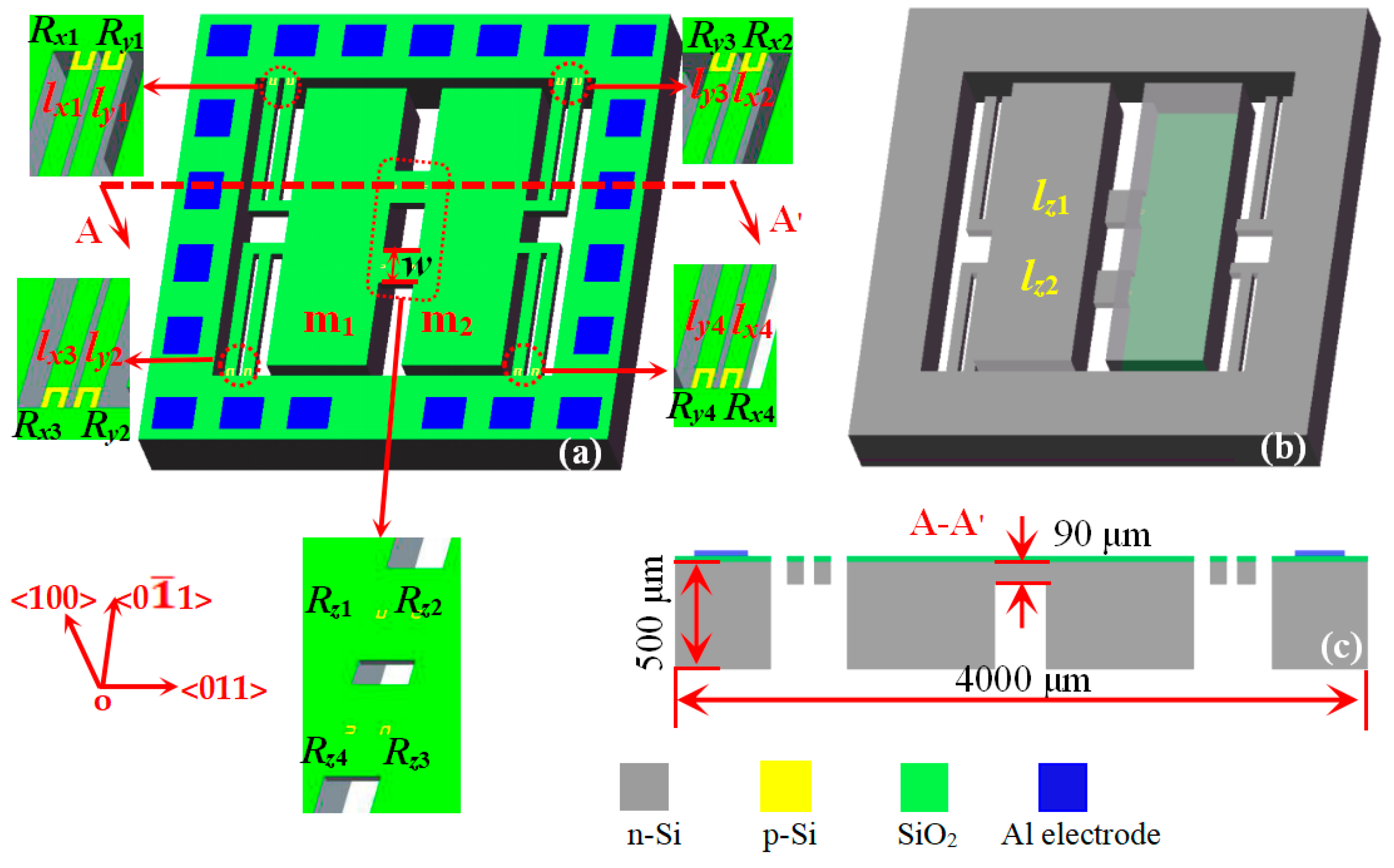
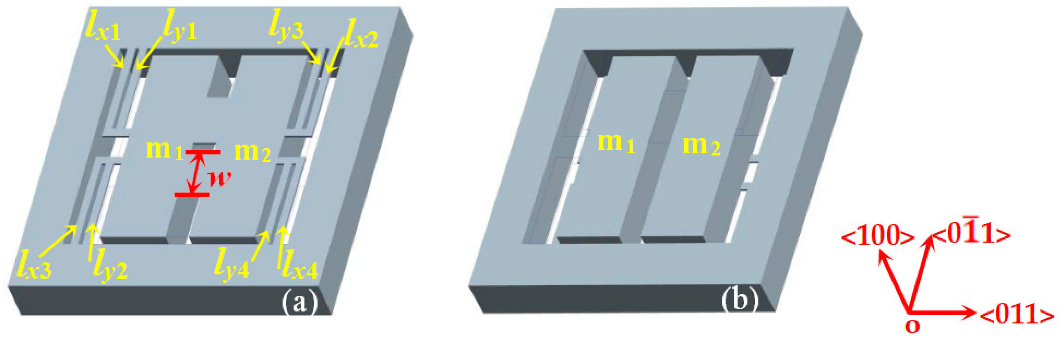
2.1. Basic Structure

The three-axis accelerometer is composed of an elastic element and a sensitive element, where the elastic element consists of four double L-shaped beams, intermediate double beams and two mass blocks, and the sensitive element has twelve piezoresistors. The basic structure of the three-axis accelerometer with double L-shaped beams is shown in Figure 1, including a top view, bottom views, as well as a cross-section view along AA’. As shown in Figure 1a,b, the two mass blocks (m1 and m2) are first connected by the intermediate double beams (lz1 and lz2) and are then connected to the support body by four double L-shaped beams (lx1, lx2, lx3, lx4, ly1, ly2, ly3 and ly4,) on a SOI wafer. Figure 1c gives the cross-section view along AA’ for the three-axis accelerometer, in which the thicknesses of the intermediate double beams are the same as those of the four double L-shaped beams.
As seen in Figure 1, the twelve piezoresistors (Rx1, Rx2, Rx3, Rx4, Ry1, Ry2, Ry3, Ry4, Rz1, Rz2, Rz3 and Rz4) were designed on the roots of four double L-shaped beams and intermediate double beams, where the four piezoresistors (Rx1, Rx2, Rx3 and Rx4) along the < 0 1 ¯ 1 > orientation are fabricated on the four L-shaped single beams (lx1, lx2, lx3 and lx4) to form a Wheatstone bridge (W1). Meanwhile, the four piezoresistors (Ry1, Ry2, Ry3 and Ry4) along the < 0 1 ¯ 1 > orientation are fabricated on the four L-shaped single beams (ly1, ly2, ly3 and ly4) to constitute a Wheatstone bridge (W2), and the other piezoresistors (Rz1, Rz2, Rz3 and Rz4) along the < 0 1 ¯ 1 > and <011> orientations are respectively fabricated on the intermediate double beams (lz1 and lz2) to form a Wheatstone bridge (W3). In order to study the effect of the width (w) of the intermediate double beams (lz1 and lz2) on the characteristics of the proposed accelerometer, six chip sizes combined with the simulation in Section 3 of this study are shown in Table 1.

2.2. Sensitivity Analysis

Figure 2 shows the equivalent circuit of the proposed three-axis accelerometer under the actions of ax, ay and az. When the supply voltage is VDD and no acceleration is applied to the chip, the output voltages of three Wheatstone bridges consisting of twelve piezoresistors are zero due to the fact that the resistances of the twelve piezoresistors are the same under ideal conditions. When exerting acceleration ax along the x-axis to the chip, the four double L-shaped beams will produce deformations. According to the piezoresistive effect of the semiconductor material, the four piezoresistors of Rx1, Rx2, Rx3 and Rx4 on the roots of lx1, lx2, lx3 and lx4 are changed, i.e., the reducing of Rx1 and Rx3 attributed to the inducted compressive stress acted on the roots of lx1 and lx3, while in contrast the increases of Rx2 and Rx4 caused by the tensile stress acted on the roots of lx2 and lx4. The absolute variations of four piezoresistors are equal in ideal conditions, named as ΔRx. Due to the fact that the output voltages Vx1 and Vx2 of W1 are relative to the acceleration along the x-axis, it is possible to realize the measurement of ax. When applying the acceleration ay along the y-axis to the chip, the four double L-shaped beams will show deformations, and Ry1, Ry2, Ry3 and Ry4 located on the roots of ly1, ly2, ly3 and ly4 are changed, resulting in the reduction of Ry1 and Ry3 due to the induced compressive stress action on the roots of ly1 and ly3, as well as in the increase of Rx2 and Rx4 caused by the tensile stress acting on the roots of ly2 and ly4. The same absolute variations of four piezoresistors in ideal conditions are regarded as ΔRy. The change of the output voltages Vy1 and Vy2 of W2 under the action of ay makes it possible to achieve the measurement of ay. In addition, when exerting the acceleration az along the z-axis to the chip, the intermediate double beams lz1 and lz2 will produce a deformation along the z-axis, and Rz1, Rz2, Rz3 and Rz4 on the roots of lz1 and lz2 are changed, indicating that Rz1 and Rz3 are influenced by compressive stress, leading to the decreases of Rz1 and Rz3 and the increases of Rz2 and Rz4. Similarly, the same absolute variations of four piezoresistors in ideal conditions are regarded as ΔRz. The changes of the output voltages Vz1 and Vz2 of W3 under the action of az contribute to the measurement of az.
When applying acceleration to the chip, the deformations of the proposed accelerometer beams would cause the variations of piezoresistors, where ∆Rx, ∆Ry, ∆Rz are the changes of piezoresistors under the actions of ax, ay and az, respectively.
In an ideal case, Rx1 = Rx2 = Rx3 = Rx4 = Rx0, Ry1 = Ry2 = Ry3 = Ry4 = Ry0, Rz1 = Rz2 = Rz3 = Rz4 = Rz0. In view of the equivalent circuit and piezoresistive effect, the relationship between the output voltages and the relative changes of piezoresistors can be expressed as follows [14]:
{ V out x = V x 1 V x 2 = Δ R x R x 0 V DD V out y = V y 1 V y 2 = Δ R y R y 0 V DD V out z = V z 1 V z 2 = Δ R z R z 0 V DD
where Rx0, Ry0 and Rz0 are the piezoresistors under no acceleration, Voutx, Vouty and Voutz are the output voltages of W1, W2, and W3, with the value of zero under the same condition.
In view of Equation (1), the output voltages of the Wheatstone bridges are directly proportional to the relative changes of the piezoresistors at a constant supply voltage. Thus, it is possible to measure the external acceleration based on the output voltage, where ΔR relative to stress is given in Equation (2) [15]:
Δ R R = π l σ l + π t σ t
where πl and πt are the longitudinal and transverse piezoresistance coefficients, and σl and σt are the longitudinal and transverse stress of the piezoresistors, respectively.
Due to the fact that the proposed accelerometer was designed on the SOI wafer with a device layer of n-type silicon with a <100> orientation, through combining Equation (1) with Equation (2), the relationship between the output voltages and the stress can be expressed as Equation (3):
{ V out x = V DD 2 π 44 ( σ l x σ t x ) V out y = V DD 2 π 44 ( σ l y σ t y ) V out z = V DD 2 π 44 ( σ l z σ t z )
where σlx and σtx are the longitudinal and transverse stress of Rx1, Rx2, Rx3 and Rx4, σly and σty are the longitudinal and transverse stress of Ry1, Ry2, Ry3 and Ry4, σlz and σtz are the longitudinal and transverse stress of Rz1, Rz2, Rz3 and Rz4, π44 is piezoresistive coefficient.
According to the sensitivity definition and sensitive principle of the three-axis accelerometer, the output voltages of the Wheatstone bridges along three axes can be expressed as Equation (4):
[ V out x V out y V out z ] = [ S x x S x y S x z S y x S y y S y z S z x S z y S z z ] [ a x a y a z ]
where Sxx, Syy and Szz are the sensitivities along the x-axis, y-axis and z-axis, respectively. Sxy and Sxz are the cross-axis sensitivities along the x-axis under ay and az, respectively. Syx and Syz are the cross-axis sensitivities along the y-axis under ax and az, respectively. Szx and Szy are the cross-axis sensitivities along the z-axis under ax and ay, respectively.
In an ideal case, the elastic deformations of the four double L-shaped beams under the action of az are identical, resulting in the same absolute variations of piezoresistors on the four double L-shaped beams, without the changes of the output voltages of W1 and W2 as well as the changes of the cross-axis sensitivities (Sxz and Syz) of the sensor. Similarly, all the cross-axis sensitivities of Syx, Szx, Szy and Sxy are zero and can be ignored. Thus, Equation (4) can be simplified as Equation (5):
[ V out x V out y V out z ] = [ S x x 0 0 0 S y y 0 0 0 S z z ] [ a x a y a z ]
Based on the above theoretical analysis, it is possible to realize the measurement of acceleration along the x-axis, y-axis and z-axis by the accelerometer. Meanwhile, the cross-axis sensitivity can be ignored by structural optimization under the ideal process conditions and the ideal environmental testing conditions, etc.

3. Simulation and Fabrication Technology

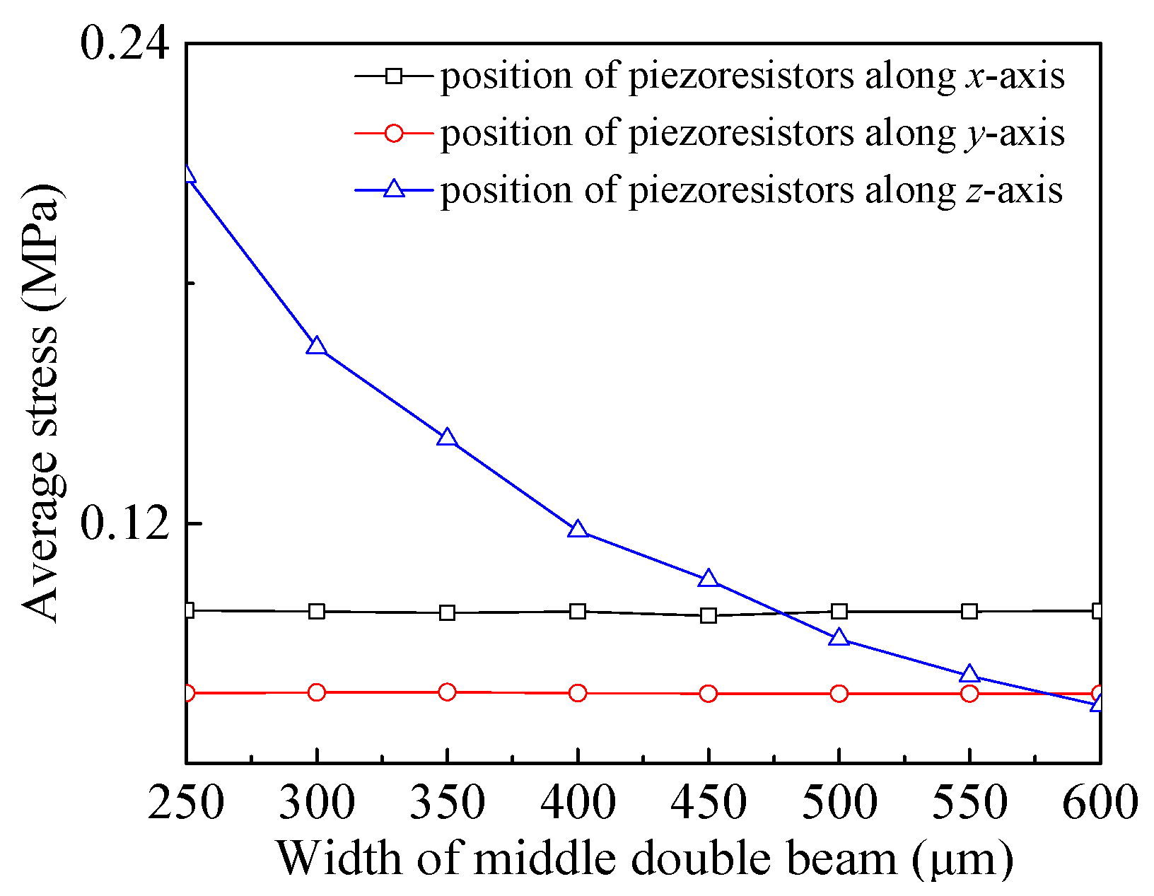
3.1. Simulation of Three-axis Accelerometer

To study how w affects the stress distribution, the finite element simulation software-Ansys 15.0 was used to simulate the characteristics of the proposed sensor, as shown in Figure 3. Figure 3a,b shows the top and bottom views of the sensor model with four double L-shaped beams, intermediate double beams and two mass blocks.
On the basis of the model, the relationship between the average stress at the piezoresistor positions on the beams and w under the actions of ax, ay and az was investigated. By respectively exerting an external acceleration of 15 g along the x-axis, y-axis and z-axis to the sensor model, six sensors (see Table 1) with different w values were simulated. Then, the average stress at the corresponding piezoresistor positions was given, as shown in Figure 4. It can be seen that the average stress at the piezoresistor positions along teh z-axis decreases with the increase of w. With respect to that, the ones along the x-axis and y-axis do not change much, as shown in Figure 4. However, when increasing w up to 500 μm, the average stress differences along the three axes are very small, and the measurement consistency is good. According to the derived equation in Section 2, it can be found that Sxx, Syy and Szz increase with the increase of the average stress, resulting in the decrease of the sensitivity along the z-axis with an increasing w. Finally, a better consistence of sensitivity is achieved when w is 500 μm.

3.2. The Fabrication Process of Three-axis Accelerometer

As shown in Figure 5, the chip was fabricated on a SOI wafer with a n-type <100> orientation device layer and resistivity of 0.1 Ω·cm by using MEMS technology, in which the insets of mask1-mask7 used for photolithography and bonding glass are given together. The synthesis procedure is illustrated as follows:
(a) Cleaning a SOI wafer using a standard cleaning method, then growing a SiO2 layer with a thickness of 50 nm by thermal oxidation method as an ion implantation buffer; (b) first, using photolithography to form an ion implantation window, performing the p+ region by utilizing ion implantation, and secondly using photolithography to etch the windows of piezoresistors, performing the p- region as piezoresistors repeating the above method. After that, placing the chip in a vacuum environment of 1000 °C for 20~30 min to activate impurity ions so as to form an impurity distribution and effectively eliminate the damage caused by the ion implantation. Etching an SiO2 layer of 50 nm using wet etching technology, and thereafter growing the SiO2 layer as an insulating layer by using plasma enhanced chemical vapor deposition (PECVD); (c) third, photolithography to etch the top surface and performing contact holes between the piezoresistors and the Al electrodes, fabricating metal Al on the top surface by a vacuum evaporation method, and fourth, photolithography to form the electrodes and interconnects, and then metalizing at 420 °C for 30 min to achieve ohmic contact; (d) growing a SiO2 layer by using PECVD as a passive layer to protect the Al electrode, and fifth, photolithography to form a pad; (e) etching the bottom surface of the chip by inductive couple plasma (ICP) technology [16] to form two mass blocks, thereafter etching the top surface of the chip by the identical technology to release four double L-shaped beams and intermediate double beams; (f) bonding a glass plate with a groove with the bottom surface of the chip by using electrostatic bonding technology to provide enough moving space for the two mass blocks.
To observe the morphology of the chip, a high-precision measuring microscope (Japan, Olympus, STM7) was used. Due to the large size (4000 μm×4000 μm) of the chip, the morphology stitching mode was used to complete the whole photograph. Figure 6a,b shows the top and bottom photographs of the fabricated chip, respectively. As shown in Figure 6a, the potential labeling of pad points on the chip corresponds to that in the equivalent circuit in Figure 2. Meanwhile, using the Dow Corning fluorosilicone solvent-resistant sealant attached the chip to the package-printed circuit board (PCB) [17]. After fully curing the sealant, bonding the leads between the chip and PCB using an integrated chip bonding machine (American, KNS, 4526) realized the connection between the solder joints on the chip and the corresponding solder joints on the PCB, as shown in Figure 6c [14].

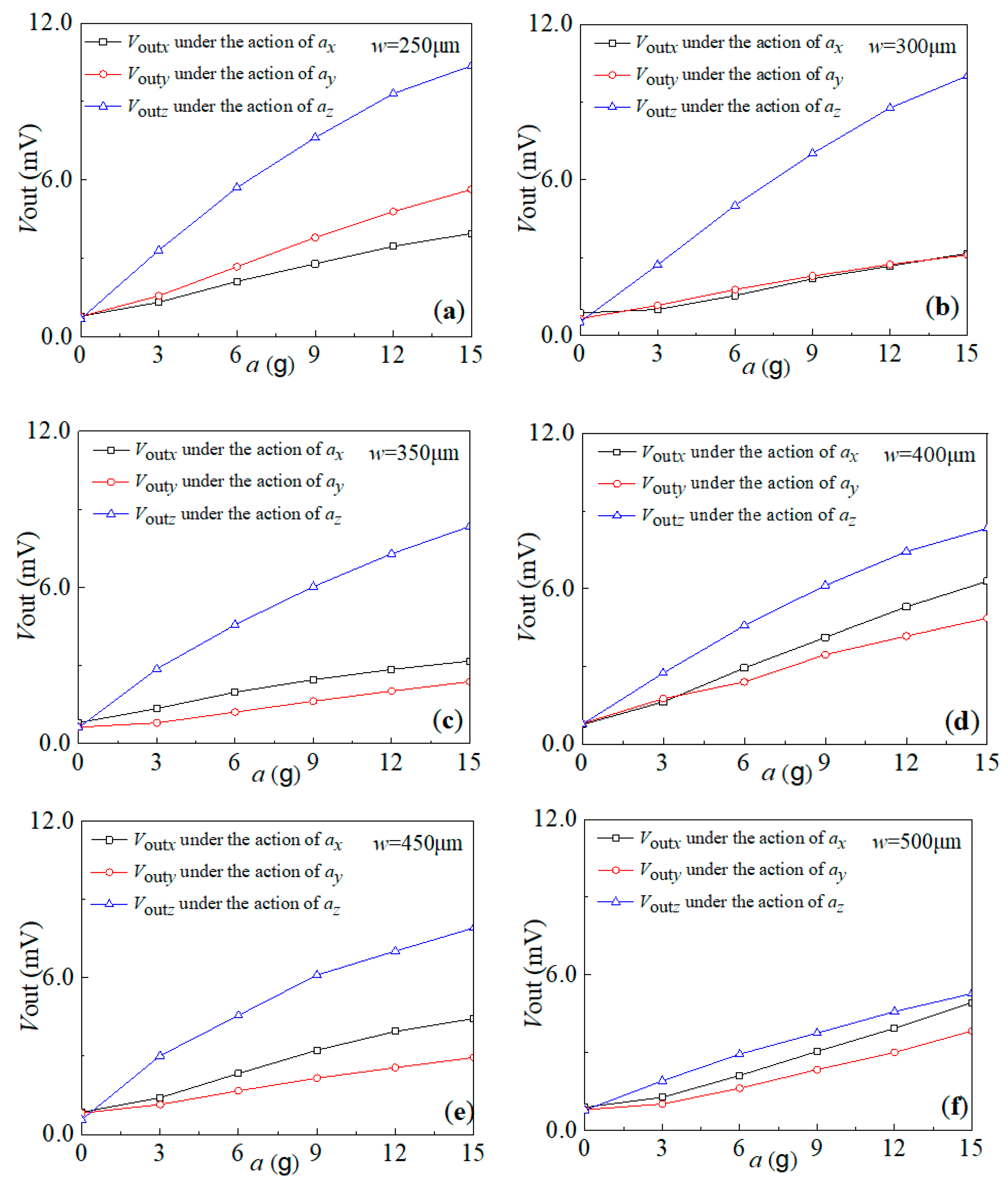
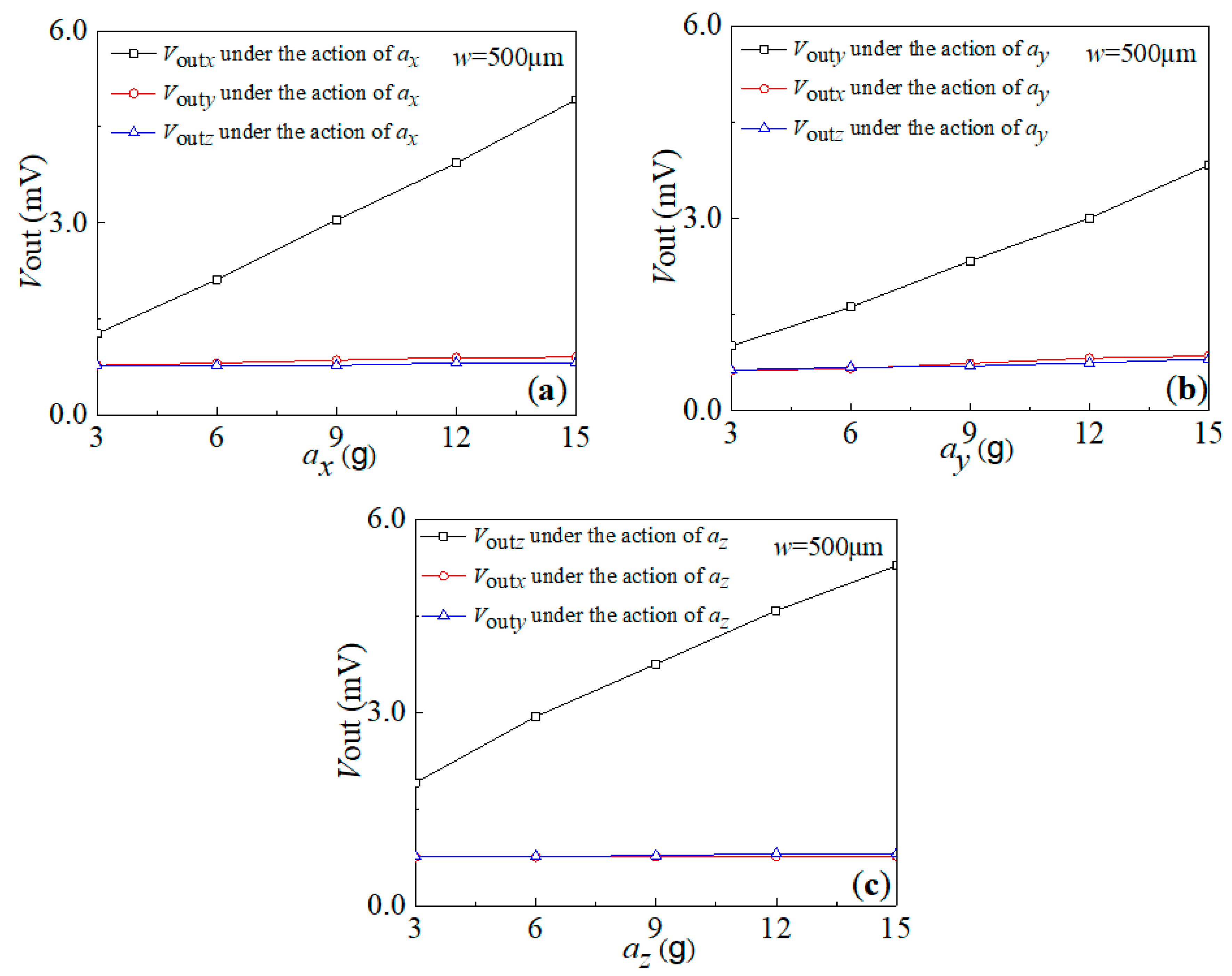
4. Results and Discussion

To study the characteristics of the three-axis accelerometer, a testing system was built, consisting of a standard vibration table (China, Dongling, ESS-050) with an excitation frequency range of 0~10,000 Hz and acceleration of 0~30 g with an accuracy of 0.1 g, a high performance digital multimeter (America, Agilent, 34410A), and a programmable linear direct-current power (China, Rigol, DP832A) to supply a voltage of 0~30 V. The test was carried out at room temperature and a humidity of 40% RH.

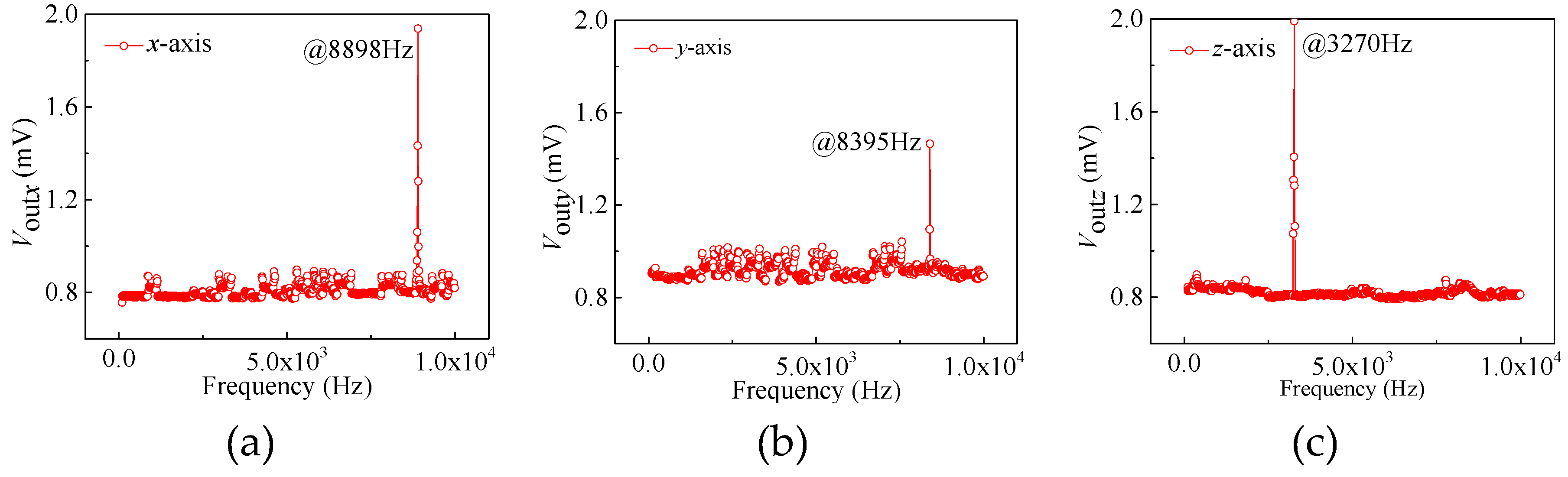
4.1. Frequency Response Characteristics

To investigate the frequency response characteristics of the six types of sensors, a frequency response characteristic test was carried out under conditions of the supply voltage of 5.0 V and an external acceleration of 3 g with a frequency range from 100 Hz to 10,000 Hz. Through taking the chip with w = 500 μm as an example, the characteristic curves of the resonance frequency along the x-axis, y-axis and z-axis are respectively shown in Figure 7a–c. As shown in Figure 7a, the test result shows that the output voltages of the sensor do not markedly change with an increase of the excitation frequency. When increasing the frequency of the excitation signal up to 8898 Hz along the x-axis, the output voltage of the sensor along the x-axis reaches a maximum. Then, the output voltage of the sensor begins to gradually decrease as the vibration frequency continually increases, thus achieving the resonance frequency of 8898 Hz along the x-axis when w = 500 μm. Similarly, when w is 500 μm the resonance frequencies along the y-axis and z-axis are 8395 Hz and 3270 Hz, as shown in Figure 7b,c. After that, a wide frequency sweep was performed on the proposed sensor, i.e., with a vibration frequency range from 100 Hz to 10,000 Hz at constant acceleration. The resonance frequencies of the six types of chips (named as AS-1~AS-6, corresponding to different w values of 250–500 μm) were obtained by observing the output voltage changes, as shown in Table 2. According to Table 2, due to the fact that the two identical mass blocks in the basic structure of the accelerometer were connected by the intermediate double beams, a collective movement can be caused to form the deformations of the double L-shaped beams, benefitting the measurement of ax or ay. However, the widths of the intermediate double beams (w) have little influence on the movement along the x-axis or y-axis, without monotonous changes of the resonance frequency along the x-axis and y-axis with w.

4.2. Sensitivity and Cross Interference Characteristics

To research the sensitivity characteristics of the six types of sensors, the sensitivity test was repeated three times under the conditions of a supply voltage of 5.0 V and acceleration along the sensitive axis from 0 g to 15 g with a step of 3 g. Figure 8 gives the relationship curves between the output voltages and the external acceleration along the three axes, where Voutx (see the black line), Vouty (see the red line) and Voutz (see the blue line) are the output voltages for the resulting sensors. As shown in Figure 8a, it can be seen that the output voltages Voutx and Vouty of the AS-1 sensor linearly increase with an increase of ax and ay, respectively. With respect to that, the output voltage Voutz of the sensor nonlinearly increases with an increase of az. In addition, when ax = ay = az, Voutz are markedly bigger than Voutx and Vouty, where Vouty is close to Voutx. This indicates that the resulting AS-1 sensor can realize the acceleration measurement along the three axes, but with a low linearity and higher sensitivity along the z-axis when compared with the other axes. As shown in Figure 8b–e, the sensors of AS-2, AS-3, AS-4 and AS-5, when compared with AS-1, have similar sensitivities and linearity along the three axes. In particular, the corresponding output voltages of the AS-6 sensor linearly increase, not only with the increasing of the external accelerations ax and ay, but also with the increasing of az, as shown in Figure 8f. In addition, when ax = ay = az, Voutx, Vouty and Voutz are close, all having a relationship curve with an approximate linearity. On the basis of this, the characteristics of the AS-6 sensor are in accord with the previous simulating results.
In addition, according to the sensitivity definition and testing data, the sensitivities of the proposed sensor with different w values are shown in Table 3. It indicates that the sensitivities of three-axis accelerometers decrease along the z-axis with the increasing widths of the intermediate double beams. When w is 500 μm, the proposed sensor achieves a better consistence of sensitivities along the three axes, with sensitivities of 0.302 mV/g, 0.235 mV/g and 0.347 mV/g, respectively.
To further study the cross-interference characteristics of the sensitivity of the AS-6 sensor, the output voltages along the three axes at constant accelerations of ax, ay and az were investigated at the same time, respectively. Figure 9 shows the relationship curves between the output voltages and the corresponding acceleration. As shown in Figure 9a, Voutx along the sensitive axis linearly increases with the increasing ax, but with slight changes in Vouty and Voutz under the same acceleration, respectively. This indicates that the Vouty and Voutz of the cross-interference caused by ax are low. Similarly, the output voltage Vouty (or Voutz) linearly increases with the increasing ay (or az), with slight changes in the other output voltages under the action of ay (or az), indicating that the Voutx and Voutz (or Voutx and Vouty) of the cross-interference caused by ay (or az) are small as well, as shown in Figure 9b,c. The test result indicates that it is possible to achieve a high output voltage along the sensitive axis and a low cross-interference along the non-sensitive axes using the AS-6 sensor.
In addition, the characteristic parameters of the AS-6 sensor are shown in Table 4. It can be seen that, when w is 500 μm, maximum and minimum cross-axis sensitivities can be achieved by the proposed sensor, i.e., 0.019 mV/g and 0.001 mV/g, respectively. According to the above data analysis, it is possible to improve the consistency of sensor sensitivity and reduce the cross-interference by using the proposed scheme.

5. Conclusions

In summary, a three-axis accelerometer with double L-shaped beams was designed and fabricated using micro-electromechanical systems (MEMS) technology in this study. When applying acceleration to the proposed sensor chip, the corresponding acceleration along the three axes could be measured according to the output voltage changes of three Wheatstone bridges based on the elastic force theory and piezoresistive effect. To investigate the characteristics of the accelerometer, the effects of the width of intermediate double beams on the characteristics were simulated to optimize the structure size. Based on that, six types of sensors with different sizes were fabricated on silicon-on-insulator (SOI) wafers using MEMS technology and were packaged on printed circuit boards (PCB) using an electrostatic bonding process and inner lead bonding technology. The test results indicate that, at room temperature and VDD = 5.0 V, better sensitivities along the three axes can be achieved by the resulting sensor with an optimized size, i.e., 0.302 mV/g, 0.235 mV/g and 0.347 mV/g, respectively. This study provides an effective fabrication method to further improve the sensitivity characteristics of three-axis accelerometers.

Author Contributions

X.Z. and D.W. conceived and designed the experiments; X.Z. and Y.W. performed the simulations and experiments; X.Z. and Y.W. analyzed the data; and X.Z. and Y.W. wrote the paper. The remaining part of the work has been done together. All authors have read and agreed to the published version of the manuscript.

Funding

This research was funded by the National Natural Science Foundation of China (Grant No. 61971180, 61471159, 61006057).

Conflicts of Interest

The authors declare no conflicts of interest

References

  1. Varanis, M.; Silva, A.; Mereles, A.; Pederiva, R. MEMS accelerometers for mechanical vibrations analysis: A comprehensive review with applications. J. Braz. Soc. Mech. Sci. Eng. 2018, 11, 527. [Google Scholar] [CrossRef]
  2. Balfas, M.; Ahamed, S.I.; Tamma, C.; Arif, M.; Kattan, A.J.; Chu, W. A Study and Estimation a Lost Person Behavior in Crowded Areas Using Accelerometer Data from Smartphones. In Proceedings of the 2018 IEEE 42nd Annual Computer Software and Applications Conference, Tokyo, Japan, 23–27 July 2018. [Google Scholar]
  3. Kapti, A.O.; Muhurcu, G. Wearable acceleration sensor application in unilateral trans-tibial amputation prostheses. Biocybern. Biomed. Eng. 2014, 34, 53–62. [Google Scholar] [CrossRef]
  4. Marco, M.; James, N.; Chrysovalantis, P. Mechanical structural design of a MEMS-based piezoresistive accelerometer for head injuries monitoring: A computational analysis by increments of the sensor mass moment of inertia. Sensors 2018, 18, 289. [Google Scholar]
  5. Theresa, L.; Oliver, G.; Alexander, B. Using MEMS acceleration sensors for monitoring blade tip movement of wind turbines. In Proceedings of the 2018 IEEE SENSORS, New Delhi, India, 28–31 October 2018. [Google Scholar]
  6. Solouk, M.R.; Shojaeefard, M.H.; Dahmarde, M. Parametric topology optimization of a MEMS gyroscope for automotive applications. Mech. Syst. Signal Process. 2019, 128, 389–404. [Google Scholar] [CrossRef]
  7. Yang, B.; Xi, J.; Yang, J.; Xue, L. An alignment method for strapdown inertial navigation systems assisted by doppler radar on a vehicle-borne moving base. Sensors 2019, 19, 4577. [Google Scholar] [CrossRef] [PubMed] [Green Version]
  8. Mohankumar, P.; Ajayan, J.; Yasodharan, R.; Devendran, P.; Sambasivam, R. A review of micromachined sensors for automotive applications. Measurement 2019, 140, 305–322. [Google Scholar] [CrossRef]
  9. Sankar, A.R.; Das, S. A very-low cross-axis sensitivity piezoresistive accelerometer with an electroplated gold layer atop a thickness reduced proof mass. Sens. Actuators A Phys. 2013, 189, 125–133. [Google Scholar] [CrossRef]
  10. Han, J.; Zhao, Z.; Niu, W.; Huang, R.; Dong, L. A low cross-axis sensitivity piezoresistive accelerometer fabricated by masked-maskless wet etching. Sens. Actuators A Phys. 2018, 283, 17–25. [Google Scholar] [CrossRef]
  11. Takahashi, H.; Kan, T.; Nakai, A.; Takahata, T.; Usami, T.; Shimoyama, I. Highly sensitive and low-crosstalk angular acceleration sensor using mirror-symmetric liquid ring channels and MEMS piezoresistive cantilevers. Sens. Actuators A Phys. 2019, 287, 39–47. [Google Scholar] [CrossRef]
  12. Bakhoum, E.G.; Cheng, M.H.M.; Kyle, R.A. 3-Axis, ultrahigh-sensitivity, miniature acceleration sensor. IEEE Trans. Compon. Packag. Manuf. Technol. 2018, 8, 244–250. [Google Scholar] [CrossRef]
  13. Zhao, X.; Li, S.; Ai, C.; Liu, H.; Wen, D. Fabrication and characterization of the Li-Doped ZnO thin films piezoelectric energy harvester with multi-resonant frequencies. Micromachines 2019, 10, 212. [Google Scholar] [CrossRef] [PubMed] [Green Version]
  14. Zhao, X.; Wen, D.; Li, G. Fabrication and characteristics of the nc-Si/c-Si heterojunction MOSFETs pressure sensor. Sensors 2012, 12, 6369–6379. [Google Scholar] [CrossRef] [PubMed] [Green Version]
  15. Singh, R.; Ngo, L.L.; Seng, H.S.; Mok, F.N.C. A silicon piezoresistive pressure sensor. In Proceedings of the First IEEE International Workshop on Electronic Design, Test and Applications ’2002, Christchurch, New Zealand, 29–31 January 2002. [Google Scholar]
  16. Munro, D. DIY MEMS; Springer: Berlin, Germany, 2019; pp. 31–47. [Google Scholar]
  17. Dong, Y.; Min, X.; Kim, W.S. A 3D-printed integrated PCB-based electochemical sensor system. IEEE Sens. J. 2018, 18, 2959–2966. [Google Scholar] [CrossRef]
Figure 1. The basic structure of the three-axis accelerometer with double L-shaped beams: (a) top view; (b) bottom view; and (c) cross-section view along AA’.
Sensors 20 01780 g001
Figure 2. The equivalent circuit of the three-axis accelerometer under the action of ax, ay and az.
Sensors 20 01780 g002
Figure 3. The structure model of the three-axis accelerometer: (a) top view; (b) bottom view.
Sensors 20 01780 g003
Figure 4. The relationship curves between the average stress at the piezoresistor positions along three axes and the width (w) of the intermediate double beams.
Sensors 20 01780 g004
Figure 5. The main fabrication process of the proposed sensor (insets of mask1-mask7 used for photolithography and bonding glass): (a) cleaning the wafer; (b) forming p+ and p- regions; (c) performing contact holes to fabricate the electrodes and interconnects; (d) forming pad; (e) ICP etching the top and bottom surfaces of the chip to release the beam structure; and (f) bonding a glass plate with the bottom surface of chip.
Sensors 20 01780 g005
Figure 6. The photograph of the proposed chip: (a) top view; (b) bottom view; and (c) packaged chip.
Sensors 20 01780 g006
Figure 7. The characteristic curves of resonance frequency when w is 500 μm: (a) along the x-axis; (b) along the y-axis; and (c) along the z-axis.
Sensors 20 01780 g007
Figure 8. The relationship curves between the output voltages of the proposed sensor and the external acceleration of the six types of sensors with different w values: (a) w = 250 μm; (b) w = 300 μm; (c) w = 350 μm; (d) w = 400 μm; (e) w = 450 μm; and (f) w = 500 μm.
Sensors 20 01780 g008
Figure 9. The cross-interference characteristic curves of the AS-6 sensor under three-axis acceleration along: (a) x-axis; (b) y-axis; (c) z-axis.
Sensors 20 01780 g009
Table 1. The parameters of the six chips with different w values.
TypeAS-1AS-2AS-3AS-4AS-5AS-6
w (μm)250300350400450500
Table 2. The resonance frequencies of the proposed sensor with different intermediate double beam widths.
Typew (μm)Resonance Frequency
along x-axis (Hz)
Resonance Frequency
along y-axis (Hz)
Resonance Frequency
along z-axis (Hz)
AS-1250910689563211
AS-2300937479633221
AS-3350778789573314
AS-4400869286943250
AS-5450799683483109
AS-6500889883953270
Table 3. The sensitivities of the proposed sensor with different widths of intermediate double beams.
Typew (μm)Sxx (mV/g)Syy (mV/g)Szz (mV/g)Linearity
(x-axis)
Linearity
(y-axis)
Linearity
(z-axis)
AS-12500.2110.3240.6463.3%2.7%9.1%
AS-23000.1350.1630.6337.6%5.4%6.8%
AS-33500.1580.1170.5157.1%5.5%7.2%
AS-44000.3690.2710.5043.0%3.2%8.3%
AS-54500.2390.1420.4705.3%3.5%10.0%
AS-65000.3020.2350.3474.1%3.4%3.4%
Table 4. The characteristic parameters of the AS-6 sensor.
Characteristic ParametersResonant Frequency (Hz)Bandwidth (Hz)Sensitivity of the Sensor along the x-axis, y-axis and z-axis
under Resonant Frequency (mV/g)
Acceleration Sensor axayaz
Sensor along x axis8898100–80000.3020.0110.004
Sensor along y axis8395100–75000.0190.2350.014
Sensor along z axis3270100–30000.0010.0040.347

