Sensors Made of Natural Renewable Materials: Efficiency, Recyclability or Biodegradability—The Green Electronics


Abstract
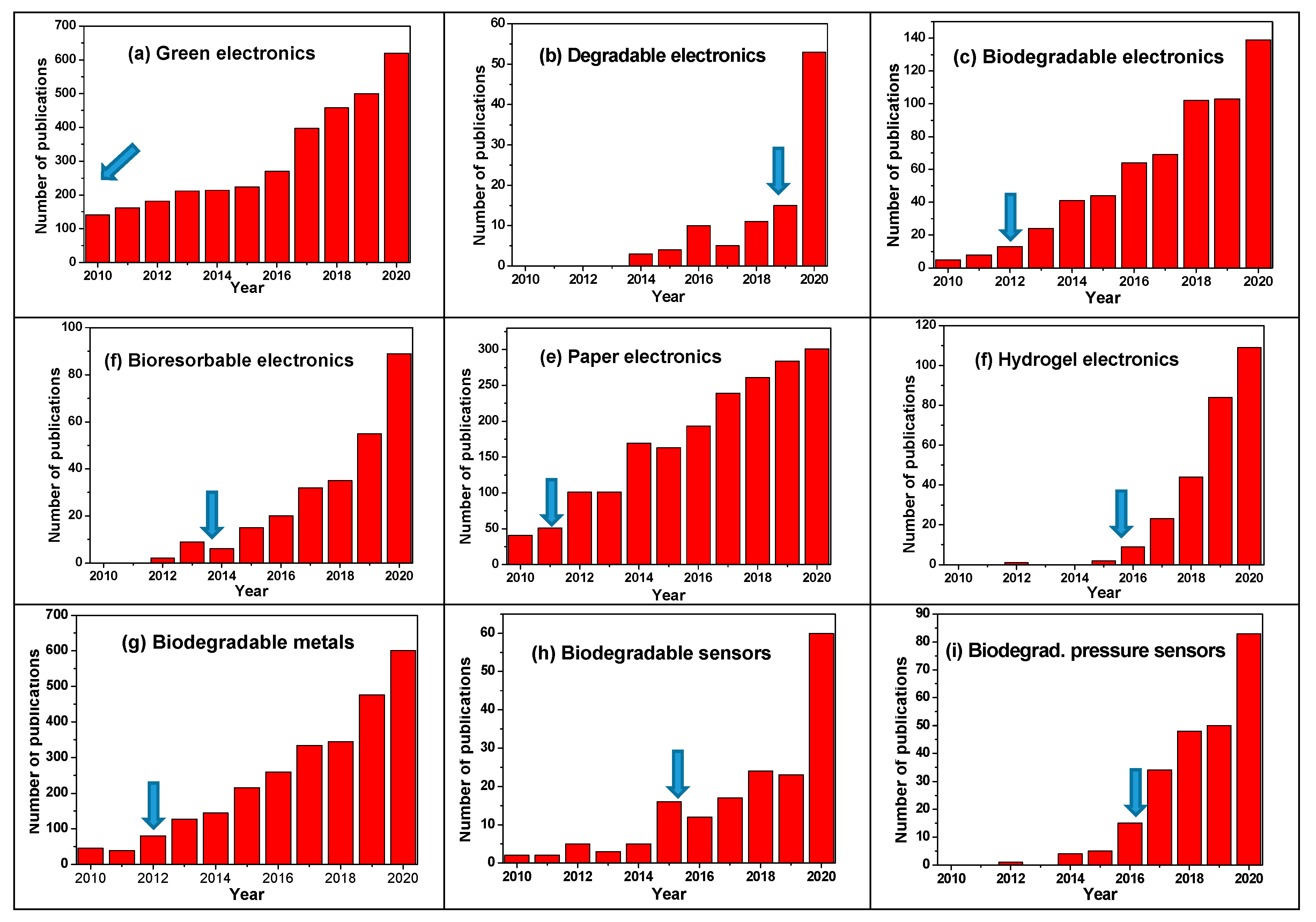
:1. Introduction
2. Discussion
2.1. Expected Outcomes
2.1.1. Definitions
2.1.2. Outcomes
Materials
Design and Fabrication Methods
2.2. Materials for Substrates, Supporting Matrices and Packaging
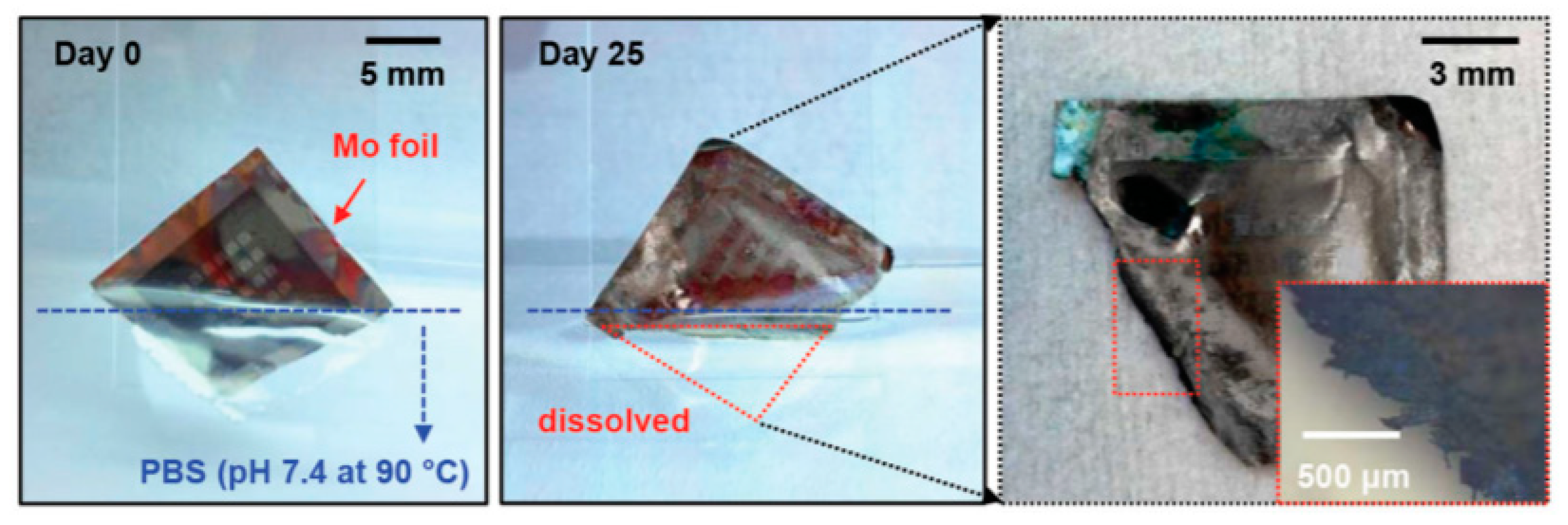
2.2.1. Inorganic Materials
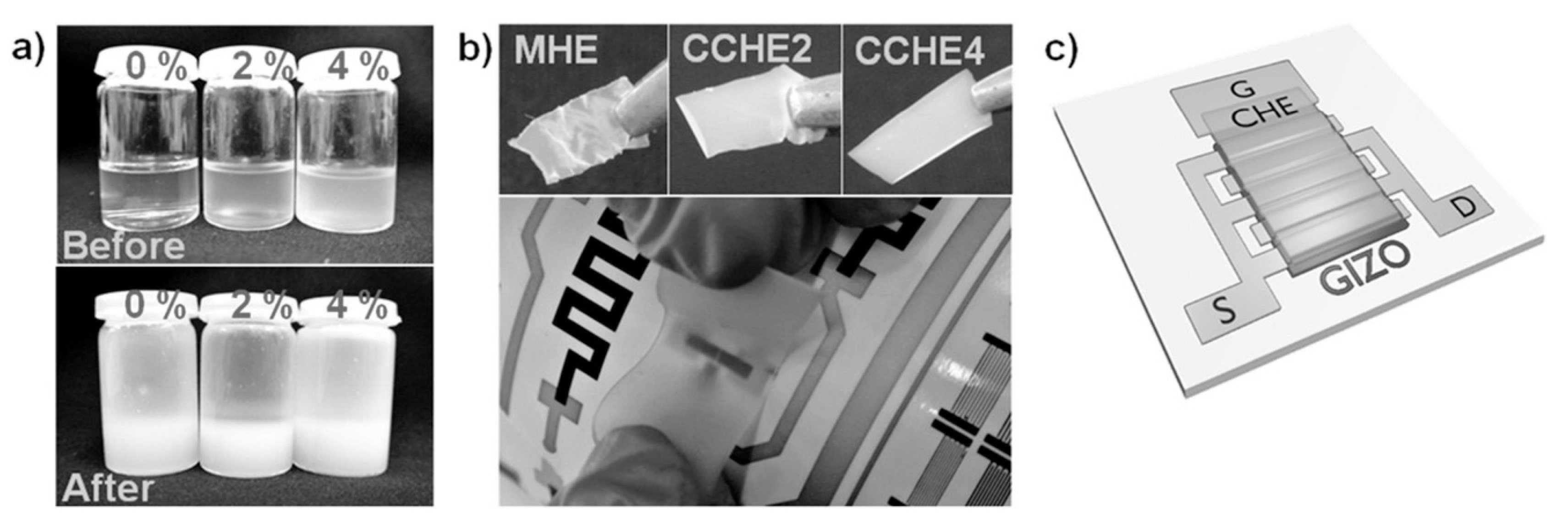
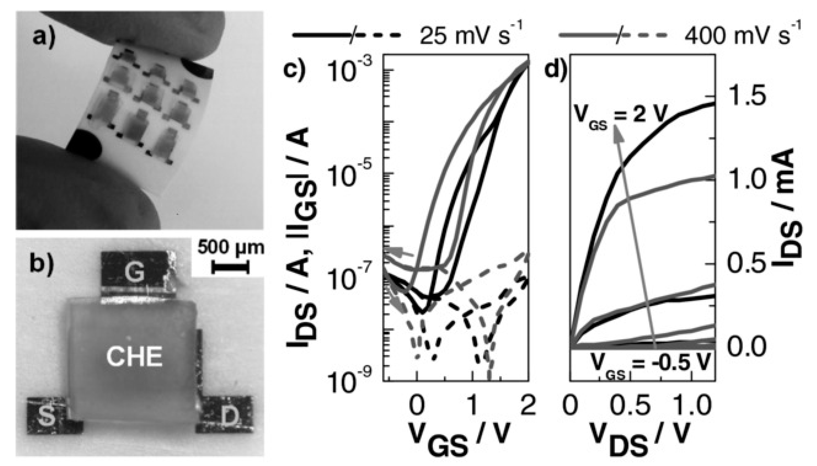
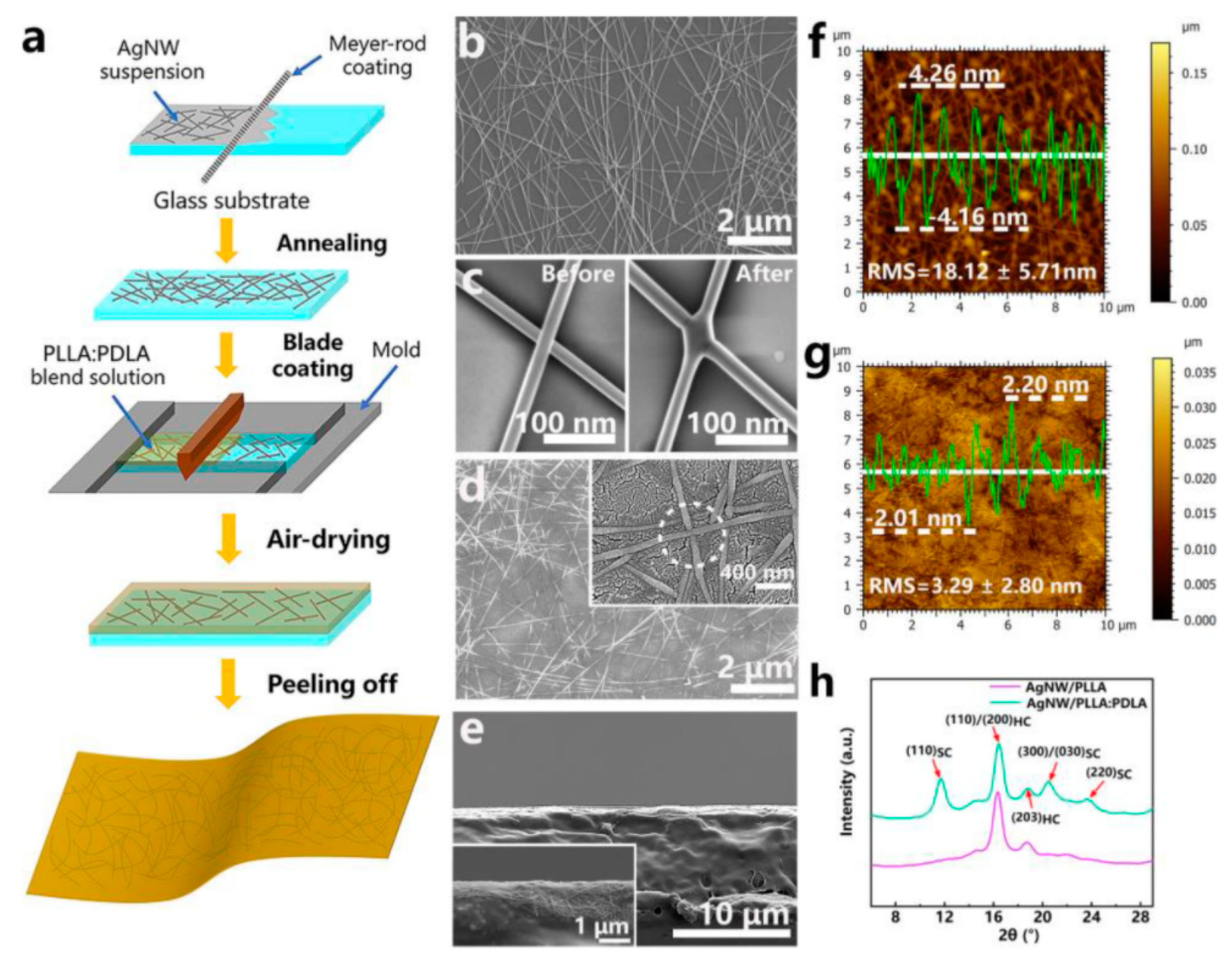
2.2.2. Organic and Hybrid Materials
2.3. Active Materials (Conductors, Semiconductors, Dielectrics)
2.3.1. Inorganic Materials
2.3.2. Organic Materials
2.4. Devices
2.4.1. Resistors and Capacitors
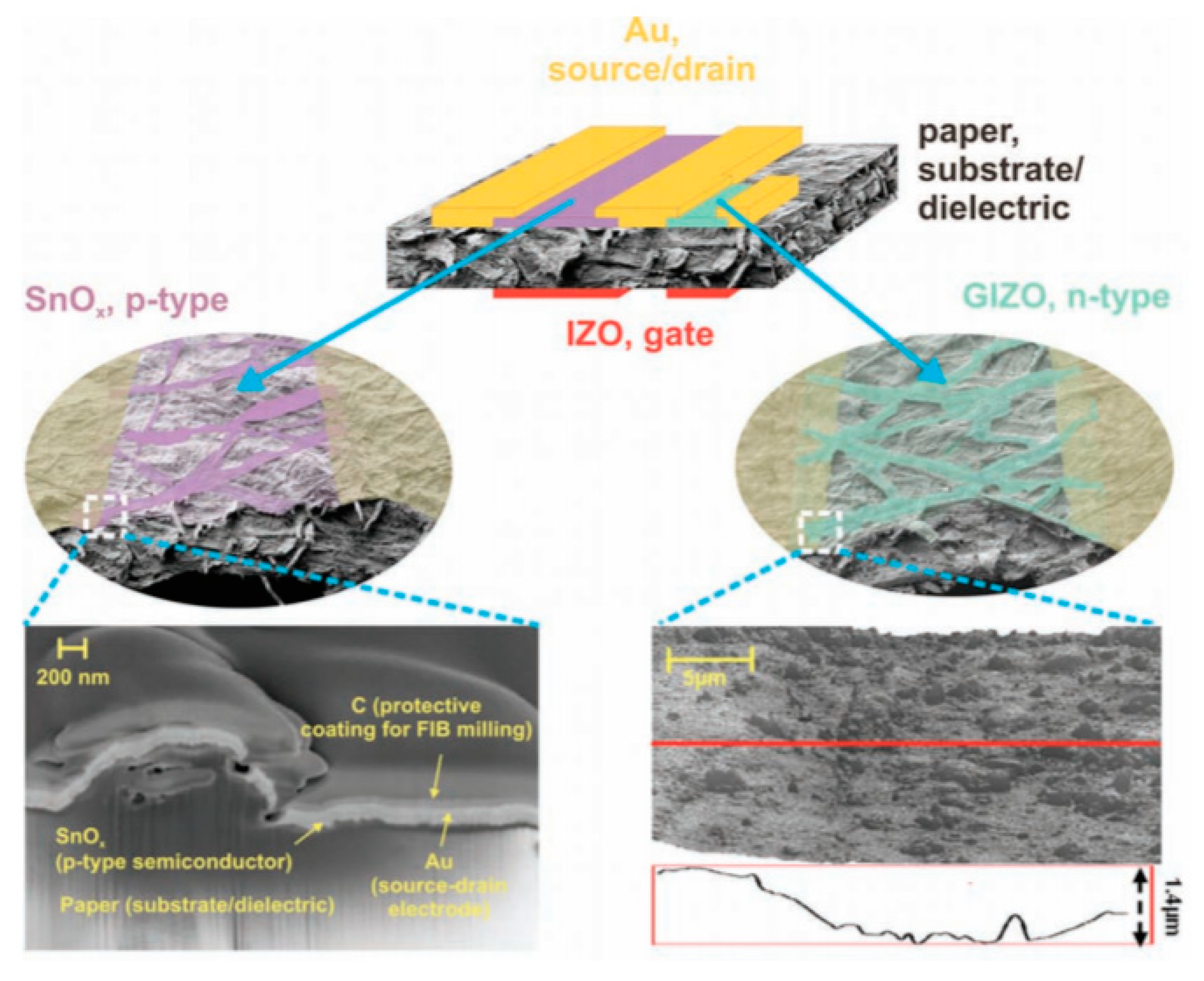
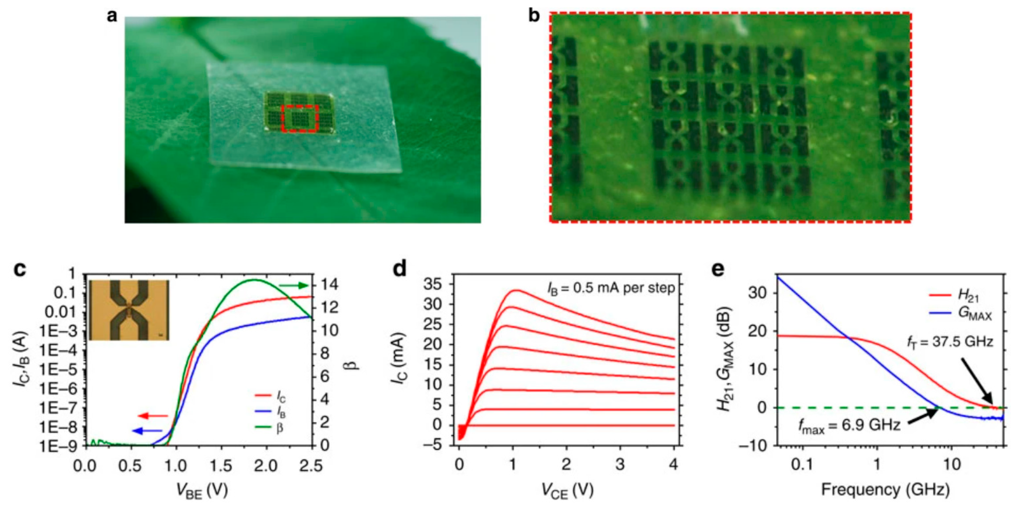
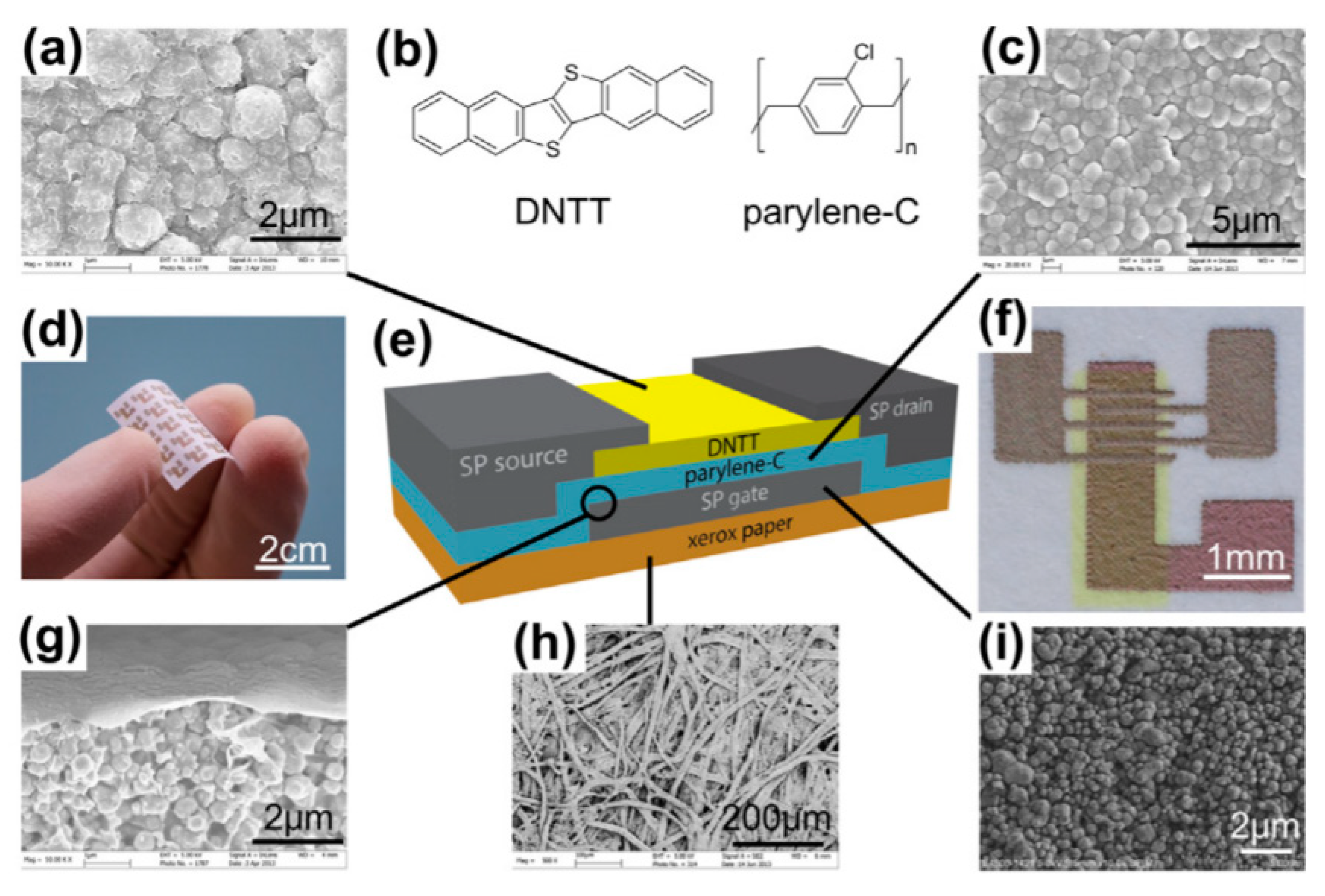
2.4.2. Transistors, Oscillators, Logic Gates
2.4.3. Antennas
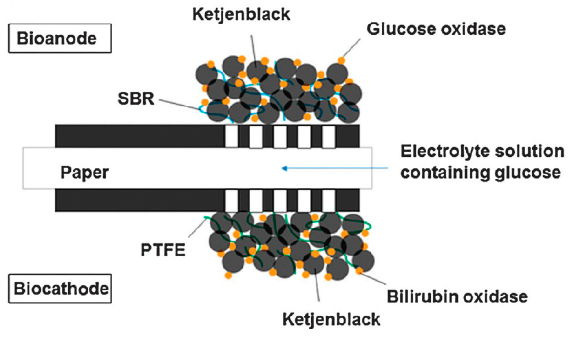
2.4.4. Biofuel Cells
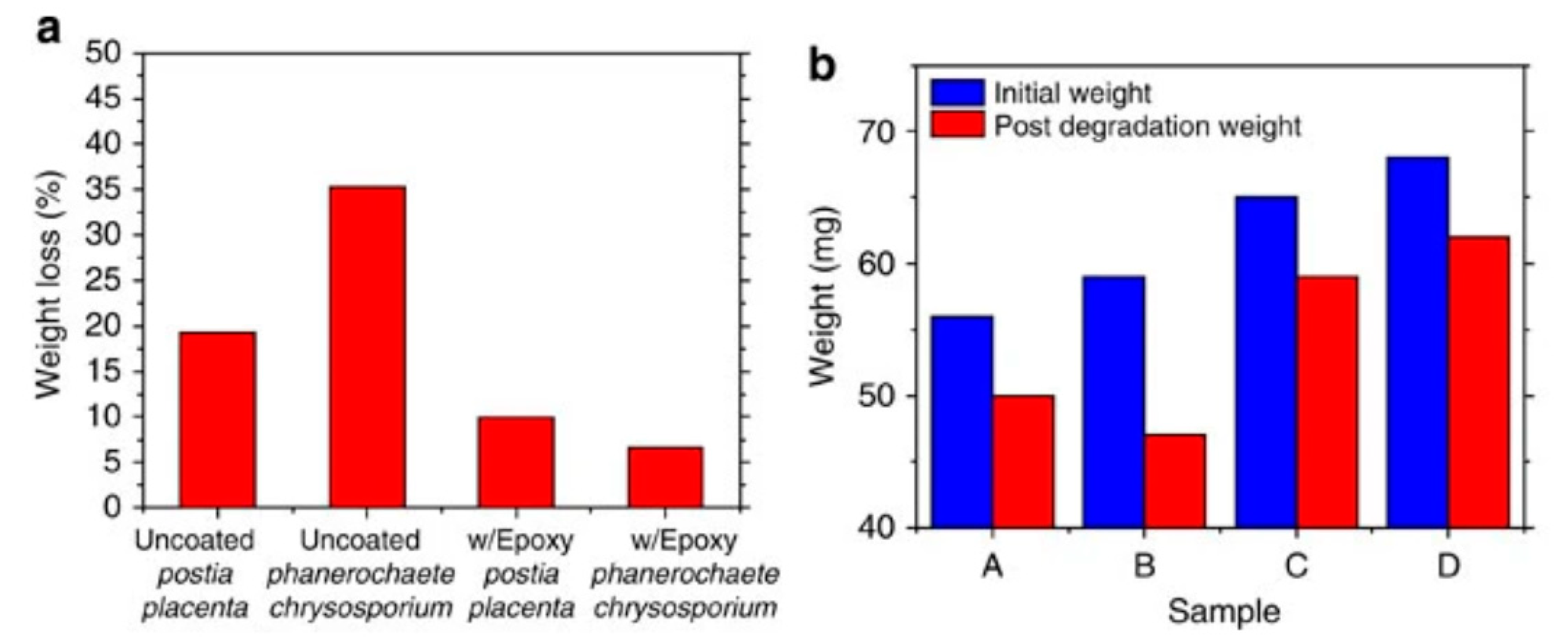
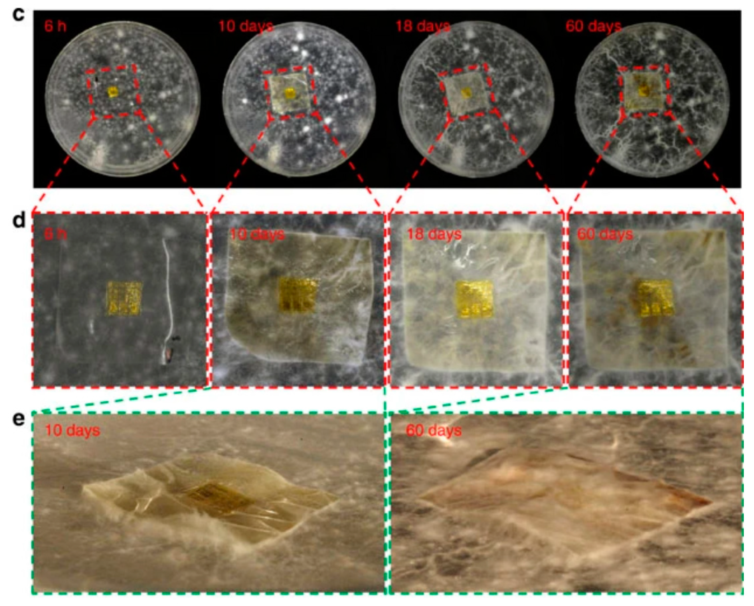
2.4.5. Sensors as a Whole
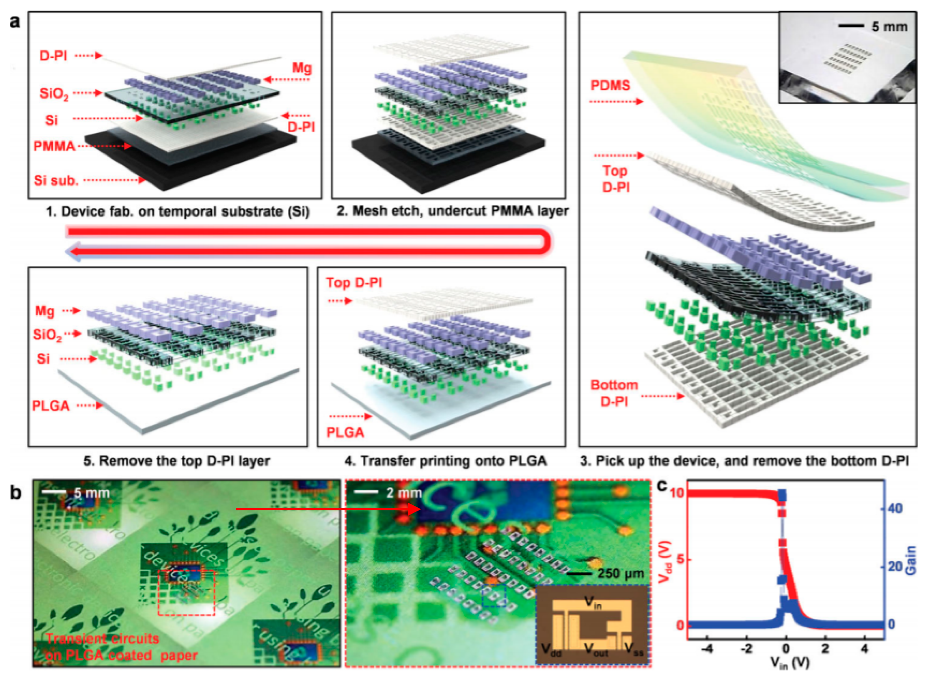
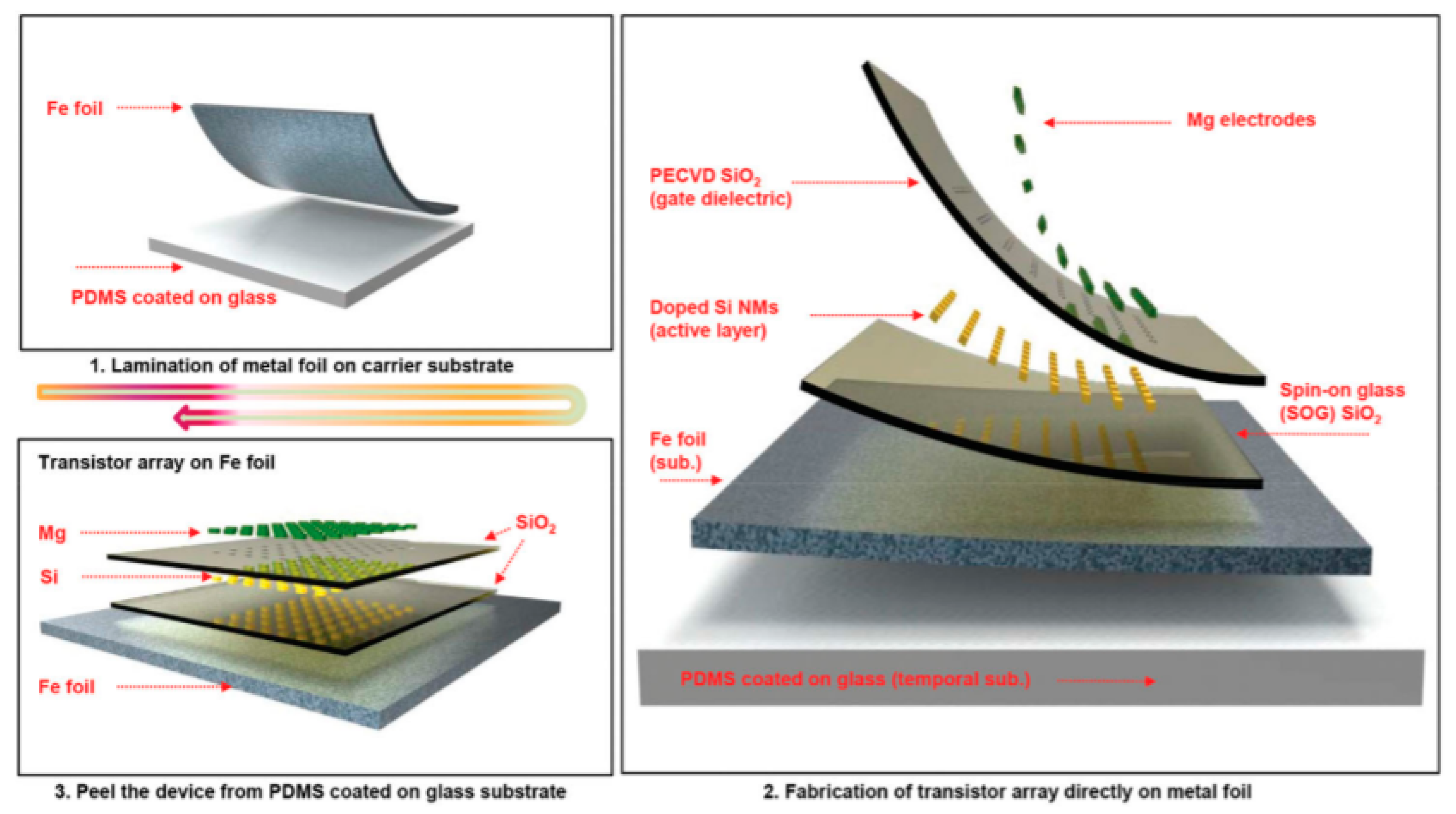
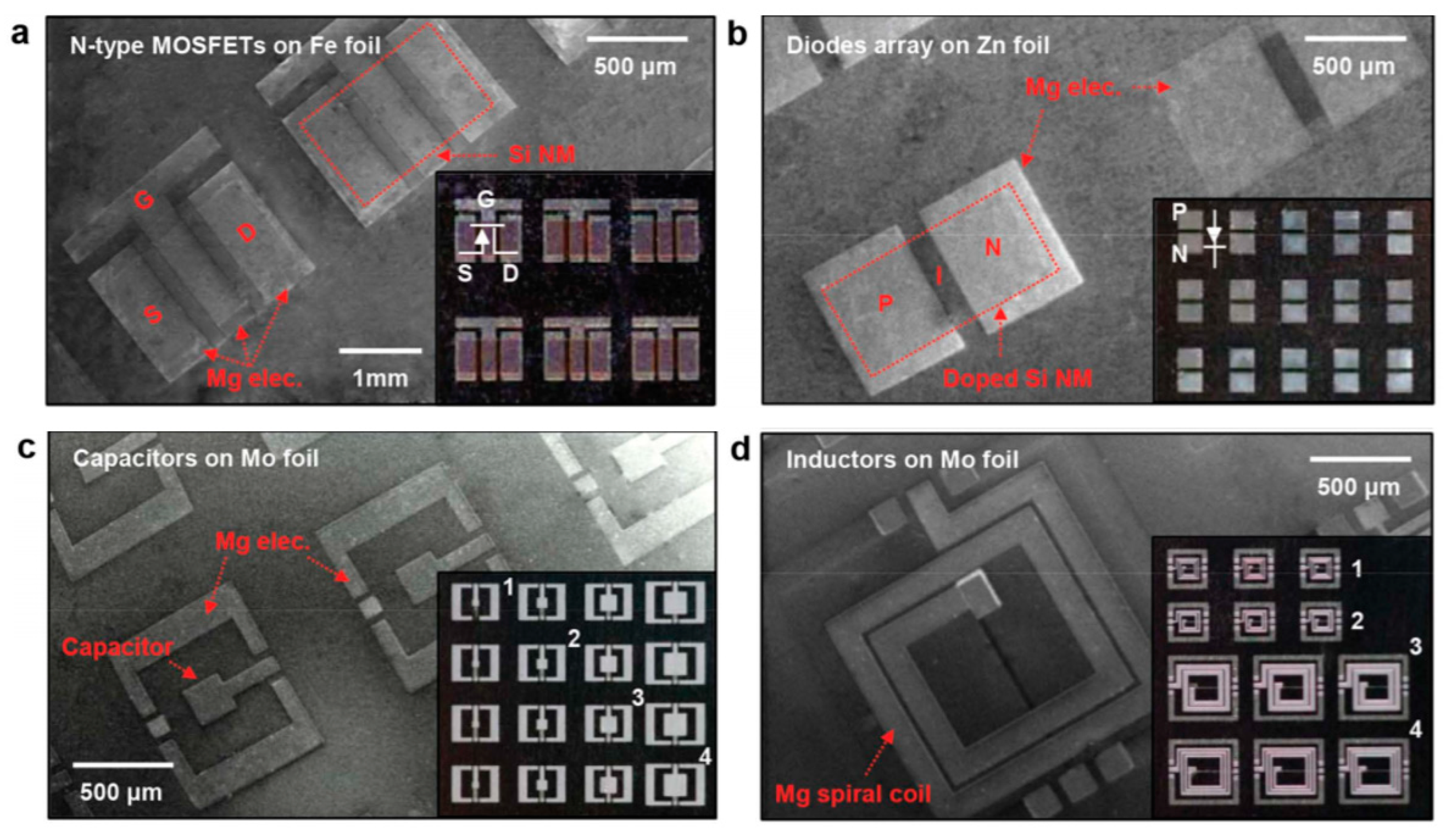
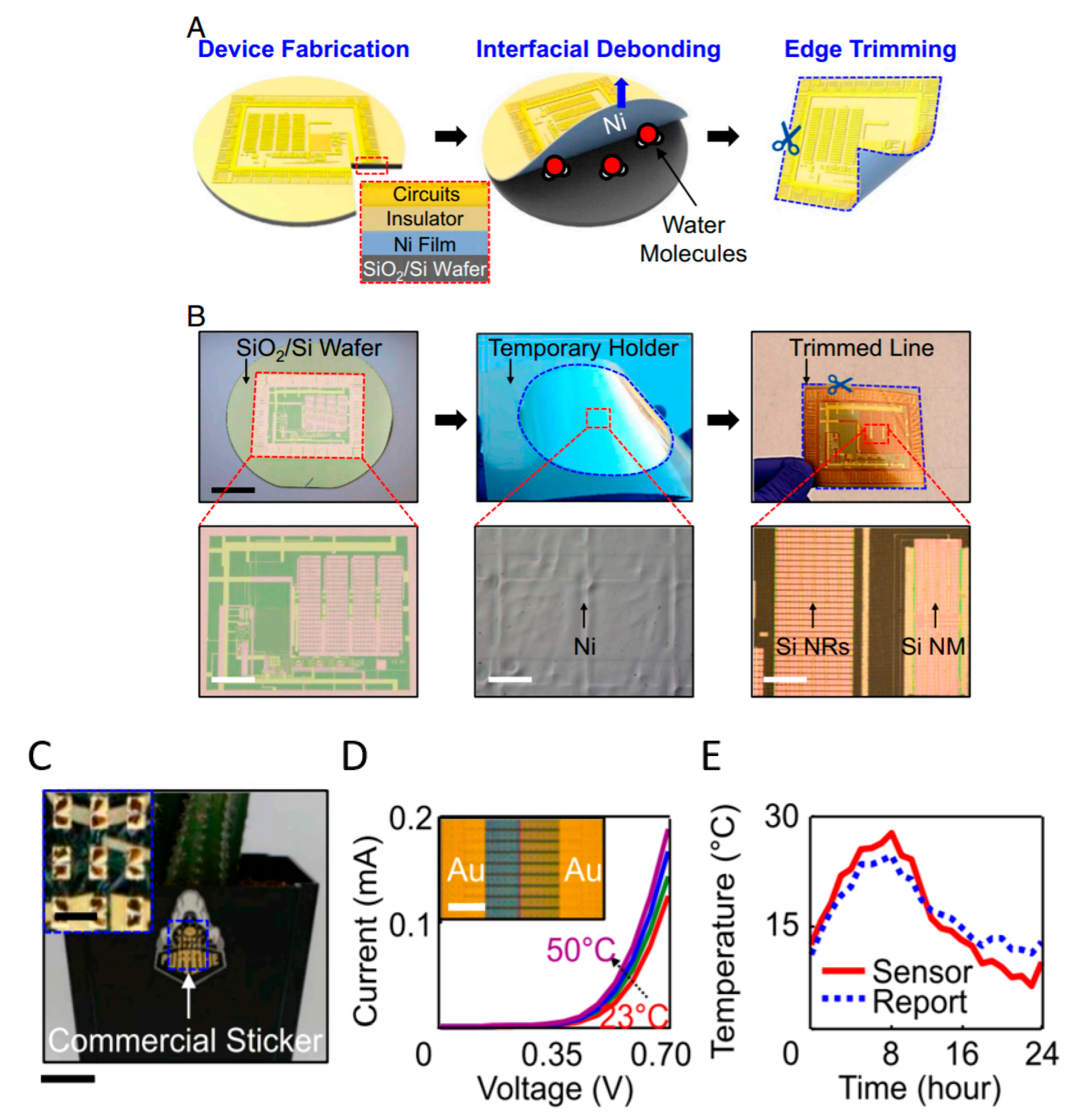
2.5. Fabrication Methods
3. Conclusions and Perspectives
Author Contributions
Funding
Acknowledgments
Conflicts of Interest
References
- Kiddee, P.; Naidu, R.; Wong, M.H. Electronic waste management approaches: An overview. Waste Manag. 2013, 33, 1237–1250. [Google Scholar] [CrossRef] [PubMed]
- Narbón-Perpiñá, I.; Prior, D. Management of Waste Electrical and Electronic Equipment in European Union Countries: A Comparison. In E-Waste Recycling and Management. Environmental Chemistry for a Sustainable World; Khan, A., Inamuddin, Asiri, A.M., Eds.; Springer: Cham, Switzerland, 2020; Volume 33. [Google Scholar] [CrossRef]
- Bauer, S.; Kaltenbrunner, M. Built To Disappear. ACS Nano 2014, 8, 5380. [Google Scholar] [CrossRef] [PubMed]
- Mühl, S.; Beyer, B. Bio-Organic Electronics—Overview and Prospects for the Future. Electronics 2014, 3, 444–461. [Google Scholar] [CrossRef] [Green Version]
- Irimia-Vladu, M.; Troshin, P.A.; Reisinger, M.; Shmygleva, L.; Kanbur, Y.; Schwabegger, G.; Bodea, M.; Schwödiauer, R.; Mumyatov, A.; Fergus, J.W.; et al. Biocompatible and Biodegradable Materials for Organic Field-Effect Transistors. Adv. Funct. Mater. 2010, 20, 4069–4076. [Google Scholar] [CrossRef]
- Irimia-Vladu, M.; Głowacki, E.D.; Voss, G.; Bauer, S.; Sariciftci, N.S. Green and biodegradable electronics. Mater. Today 2012, 15, 340–346. [Google Scholar] [CrossRef]
- Irimia-Vladu, M. Green electronics: Biodegradable and biocompatible materials and devices for sustainable future. Chem. Soc. Rev. 2014, 43, 588–610. [Google Scholar] [CrossRef] [Green Version]
- Ponnamma, D.; Parangusan, H.; Deshmukh, K.; Kar, P.; Muzaffar, A.; Pasha, S.K.K.; Al-Maadeed, M.A.A. Green synthesized materials for sensor, actuator, energy storage and energy generation: A review. Polym. Plast. Technol. Mater. 2020, 59, 1–62. [Google Scholar] [CrossRef]
- La Mattina, A.A.; Mariani, S.; Barillaro, G. Bioresorbable Materials on the Rise: From Electronic Components and Physical Sensors to In Vivo Monitoring Systems. Adv. Sci. 2020, 7, 1902872. [Google Scholar] [CrossRef] [Green Version]
- Erne, P.; Schier, M.; Resink, T.J. The road to bioabsorbable stents: Reaching clinical reality? Cardiovasc. Interv. Radiol. 2006, 29, 11–16. [Google Scholar] [CrossRef]
- Tan, L.; Yu, X.; Wan, P.; Yang, K. Biodegradable materials for bone repairs: A review. J. Mater. Sci. Technol. 2013, 29, 503–513. [Google Scholar] [CrossRef]
- Gray, M.; Meehan, J.; Ward, C.; Langdon, S.P.; Kunkler, I.H.; Murray, A.; Argyle, D. Implantable biosensors and their contribution to the future of precision medicine. Vet. J. 2018, 239, 21. [Google Scholar] [CrossRef] [PubMed]
- Rong, G.; Corrie, S.R.; Clark, H.A. In Vivo Biosensing: Progress and Perspectives. ACS Sens. 2017, 2, 327. [Google Scholar] [CrossRef] [PubMed]
- Kim, J.; Campbell, A.S.; de Ávila, B.E.F.; Wang, J. Wearable biosensors for healthcare monitoring. Nat. Biotechnol. 2019, 37, 389. [Google Scholar] [CrossRef] [PubMed]
- Lopez Hernandez, H.; Kang, S.K.; Lee, O.P.; Hwang, S.W.; Kaitz, J.A.; Inci, B.; Park, C.W.; Chung, S.; Sottos, N.R.; Moore, J.S.; et al. Triggered Transience of Metastable Poly(phthalaldehyde) for Transient Electronics. Adv. Mater. 2014, 26, 7637. [Google Scholar] [CrossRef]
- Park, C.W.; Kang, S.K.; Hernandez, H.L.; Kaitz, J.A.; Wie, D.S.; Shin, J.; Lee, O.P.; Sottos, N.R.; Moore, J.S.; Rogers, J.A.; et al. Thermally Triggered Degradation of Transient Electronic Devices. Adv. Mater. 2015, 27, 3783. [Google Scholar] [CrossRef]
- Kang, S.K.; Koo, J.; Lee, Y.K.; Rogers, J.A. Advanced Materials and Devices for Bioresorbable Electronics. Acc. Chem. Res. 2018, 51, 988–998. [Google Scholar] [CrossRef]
- Cao, Y.; Uhrich, K.E. Biodegradable and biocompatible polymers for electronic applications: A review. J. Bioact. Compat. Pol. 2019, 34, 3–15. [Google Scholar] [CrossRef]
- Feig, V.R.; Tran, H.; Bao, Z. Biodegradable Polymeric Materials in Degradable Electronic Devices. ACS Cent. Sci. 2018, 4, 337–348. [Google Scholar] [CrossRef] [Green Version]
- Liu, H.; Jian, R.; Chen, H.; Tian, X.; Sun, C.; Zhu, J.; Yang, Z.; Sun, J.; Wang, C. Application of Biodegradable and Biocompatible Nanocomposites in Electronics: Current Status and Future Directions. Nanomaterials 2019, 9, 950. [Google Scholar] [CrossRef] [Green Version]
- Li, X.; Ding, C.; Li, X.; Yang, H.; Liu, S.; Wang, X.; Zhang, L.; Sun, Q.; Liu, X.; Chen, J. Electronic biopolymers: From molecular engineering to functional devices. Chem. Eng. J. 2020, 397, 125499. [Google Scholar] [CrossRef]
- Baumgartner, M.; Coppola, M.E.; Sariciftci, N.S.; Glowacki, E.D.; Bauer, S.; Irimia-Vladu, M. Emerging Green Materials and Technologies for Electronics. In Green Materials for Electronics; Irimia-Vladu, M., Glowacki, E.D., Sariciftci, N.S., Bauer, S., Eds.; Wiley-VCH: Weinheim, Germany, 2017. [Google Scholar] [CrossRef]
- Le Borgne, B.; Chung, B.-Y.; Tas, M.O.; King, S.G.; Harnois, M.; Sporea, R.A. Eco-Friendly Materials for Daily-Life Inexpensive Printed Passive Devices: Towards “Do-It-Yourself” Electronics. Electronics 2019, 8, 699. [Google Scholar] [CrossRef] [Green Version]
- Fu, K.K.; Wang, Z.; Dai, J.; Carter, M.; Hu, L. Transient Electronics: Materials and Devices. Chem. Mater. 2016, 28, 3527–3539. [Google Scholar] [CrossRef]
- Tan, M.J.; Owh, C.; Chee, P.L.; Kyaw, A.K.K.; Kai, D.; Loh, X.J. Biodegradable electronics: Cornerstone for sustainable electronics and transient applications. J. Mater. Chem. C 2016, 4, 5531. [Google Scholar] [CrossRef]
- Li, W.; Liu, Q.; Zhang, Y.; Li, C.; He, Z.; Choy, W.C.H.; Low, P.J.; Sonar, P.; Kyaw, A.K.K. Biodegradable Materials and Green Processing for Green Electronics. Adv. Mater. 2020, 2001591. [Google Scholar] [CrossRef]
- Kuzma, M.; Gerhard, E.; Shan, D.; Yang, J. Advances in Bioresorbable Electronics and Uses in Biomedical Sensing. In Interfacing Bioelectronics and Biomedical Sensing; Cao, H., Coleman, T., Hsiai, T.K., Khademhosseini, A., Eds.; Springer: Cham, Switzerland, 2020; pp. 29–72. [Google Scholar] [CrossRef]
- Cheng, H. Inorganic Dissolvable Bioelectronics. In Interfacing Bioelectronics and Biomedical Sensing; Cao, H., Coleman, T., Hsiai, T.K., Khademhosseini, A., Eds.; Wiley-VCH: Weinheim, Germany, 2020; pp. 73–100. [Google Scholar] [CrossRef]
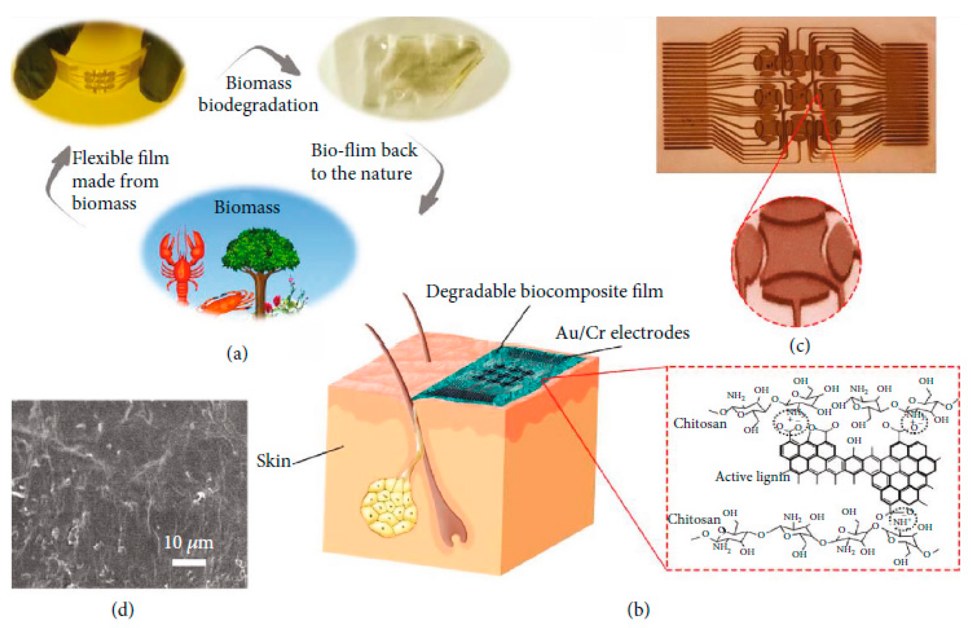
- Bhat, V.S.; Supriya, S.; Hegde, G. Biomass Derived Carbon Materials for Electrochemical Sensors. J. Electrochem. Soc. 2019, 167, 037526. [Google Scholar] [CrossRef]
- Hu, B.; Wang, K.; Wu, L.; Yu, S.H.; Antonietti, M.; Titirici, M.M. Engineering Carbon Materials from the Hydrothermal Carbonization Process of Biomass. Adv. Mater. 2010, 22, 813–828. [Google Scholar] [CrossRef]
- Wang, L.; Zhang, Q.; Chen, S.; Xu, F.; Chen, S.; Jia, J.; Tan, H.; Hou, H.; Song, Y. Electrochemical Sensing and Biosensing Platform Based on Biomass-Derived Macroporous Carbon Materials. Anal. Chem. 2014, 86, 1414–1421. [Google Scholar] [CrossRef]
- Li, X.; Zhu, X.Q.; Okuda, K.; Zhang, Z.; Ashida, R.; Yao, H.; Miura, K. Preparation of carbon fibers from low-molecular-weight compounds obtained from low-rank coal and biomass by solvent extraction. New Carbon Mater. 2017, 32, 41–47. [Google Scholar] [CrossRef]
- Meng, W.; Bai, X.; Wang, B.; Liu, Z.; Lu, S.; Yang, B. Biomass-Derived Carbon Dots and Their Applications. Energy Environ. Mater. 2019, 2, 172–192. [Google Scholar] [CrossRef]
- Liu, M.L.; Chen, B.B.; Li, C.M.; Huang, C.Z. Carbon dots: Synthesis, formation mechanism, fluorescence origin and sensing applications. Green Chem. 2019, 21, 449–471. [Google Scholar] [CrossRef]
- Kim, M.I.; Lee, Y.S. A Comprehensive Review of Gas Sensors Using Carbon Materials. J. Nanosci. Nanotechnol. 2016, 16, 4310–4319. [Google Scholar] [CrossRef] [PubMed]
- Han, T.; Nag, A.; Mukhopadhyay, S.C.; Xu, Y. Carbon nanotubes and its gas-sensing applications: A review. Sens. Actuators A Phys. 2019, 291, 107–143. [Google Scholar] [CrossRef]
- Tulliani, J.M.; Inserra, B.; Ziegler, D. Carbon-based materials for humidity sensing: A short review. Micromachines 2019, 10, 232. [Google Scholar] [CrossRef] [PubMed] [Green Version]
- Yan, T.; Wang, Z.; Pan, Z.J. Flexible strain sensors fabricated using carbon-based nanomaterials: A review. Curr. Opin. Solid State Mater. Sci. 2018, 22, 213–228. [Google Scholar] [CrossRef]
- Asadian, E.; Ghalkhani, M.; Shahrokhian, S. Electrochemical sensing based on carbon nanoparticles: A review. Sens. Actuators B Chem. 2019, 293, 183–209. [Google Scholar] [CrossRef]
- Jian, M.; Wang, C.; Wang, Q.; Wang, H.; Xia, K.; Yin, Z.; Zhang, Y. Advanced carbon materials for flexible and wearable sensors. Sci. China Mater. 2017, 60, 1026–1062. [Google Scholar] [CrossRef]
- Xu, X.; Niu, X.; Wu, S.; Zou, X.; Pan, J. A detachable and recyclable electrochemical sensor for high-performance detection of glucose based on boronate affinity. Sens. Actuators B 2018, 268, 430–437. [Google Scholar] [CrossRef]
- Wu, S.; He, Q.; Zhou, C.; Qi, X.; Huang, X.; Yin, Z.; Yang, Y.; Zhang, H. Synthesis of Fe3O4 and Pt nanoparticles on reduced graphene oxide and their use as a recyclable catalyst. Nanoscale 2012, 4, 2478. [Google Scholar] [CrossRef]
- Wu, S.; He, Q.; Zhou, C.; Qi, X.; Huang, X.; Yin, Z.; Yang, Y.; Zhang, H. Recyclable enzyme mimic of cubic Fe3O4 nanoparticles loaded on graphene oxide-dispersed carbon nanotubes with enhanced peroxidase-like catalysis and electrocatalysis. J. Mater. Chem. B 2014, 2, 4442. [Google Scholar] [CrossRef]
- Zhang, Y.; Su, Z.; Li, B.; Zhang, L.; Fan, D.; Ma, H. Recyclable Magnetic Mesoporous Nanocomposite with Improved Sensing Performance toward Nitrite. ACS Appl. Mater. Interfaces 2016, 8, 12344–12351. [Google Scholar] [CrossRef]
- Kang, S.K.; Hwang, S.W.; Yu, S.; Seo, J.H.; Corbin, E.A.; Shin, J.; Wie, D.S.; Bashir, R.; Ma, Z.; Rogers, J.A. Biodegradable Thin Metal Foils and Spin-On Glass Materials for Transient Electronics. Adv. Funct. Mater. 2015, 25, 1789–1797. [Google Scholar] [CrossRef]
- Martins, R.F.P.; Ahnood, A.; Correia, N.; Pereira, L.M.N.P.; Barros, R.; Barquinha, P.M.C.B.; Costa, R.; Ferreira, I.M.M.; Nathan, A.; Fortunato, E.E.M.C. Recyclable, Flexible, Low-Power Oxide Electronics. Adv. Funct. Mater. 2013, 23, 2153–2161. [Google Scholar] [CrossRef]
- Valentini, L.; Kenny, J.M.; Alimenti, F.; Roselli, L. Planar MOSFET devices on paper substrate using graphene oxide film as gate dielectric. In Proceedings of the 2013 European Microwave Conference, Nuremberg, Germany, 6–10 October 2013; pp. 5–8. [Google Scholar] [CrossRef]
- Yang, G.; Lee, C.; Kim, J.; Ren, F.; Pearton, S.J. Flexible graphene-based chemical sensors on paper substrates. Phys. Chem. Chem. Phys. 2013, 15, 1798–1801. [Google Scholar] [CrossRef] [PubMed]
- Peng, B.; Ren, X.; Wang, Z.; Wang, X.; Roberts, R.C.; Chan, P.K.L. High performance organic transistor active-matrix driver developed on paper substrate. Sci. Rep. 2014, 4, 6430. [Google Scholar] [CrossRef] [PubMed] [Green Version]
- Jung, Y.H.; Chang, T.; Zhang, H.; Yao, C.; Zheng, Q.; Yang, V.W.; Mi, H.; Kim, M.; Cho, S.J.; Park, D.W.; et al. High-performance green flexible electronics based on biodegradable cellulose nanofibril paper. Nat. Commun. 2015, 6, 7170. [Google Scholar] [CrossRef]
- Kanaparthi, S.; Badhulika, S. Eco-friendly all-carbon paper electronics fabricated by a solvent-free drawing method. Nanotechnology 2016, 27, 095206. [Google Scholar] [CrossRef]
- Guna, V.K.; Murugesan, G.; Basavarajaiah, B.H.; Llangovan, M.; Olivera, S.; Krishna, V.; Reddy, N. Plant-Based Completely Biodegradable Printed Circuit Boards. IEEE Trans. Electron Devices 2016, 63, 4893–4898. [Google Scholar] [CrossRef]
- Liu, H.; Li, J.; Tan, R. Flexible In2O3 Nanowire Transistors on Paper Substrates. IEEE J. Electron Devices Soc. 2017, 5, 141–144. [Google Scholar] [CrossRef]
- Zschieschang, U.; Klauk, H. Organic transistors on paper: A brief review. J. Mater. Chem. C 2019, 7, 5522–5533. [Google Scholar] [CrossRef] [Green Version]
- Zhu, H.; Luo, W.; Ciesielski, P.N.; Fang, Z.; Zhu, J.Y.; Henriksson, G.; Himmel, M.E.; Hu, L. Wood-Derived Materials for Green Electronics, Biological Devices, and Energy Applications. Chem. Rev. 2016, 116, 9305–9374. [Google Scholar] [CrossRef]
- Fu, Q.; Chen, Y.; Sorieul, M. Wood-Based Flexible Electronics. ACS Nano 2020, 14, 3528–3538. [Google Scholar] [CrossRef] [PubMed]
- Gaspar, D.; Fernandes, S.N.; de Oliveira, A.G.; Fernandes, J.G.; Grey, P.; Pontes, R.V.; Pereira, L.; Martins, R.; Godinho, M.H.; Fortunato, E. Nanocrystalline cellulose applied simultaneously as the gate dielectric and the substrate in flexible field effect transistors. Nanotechnology 2014, 25, 094008. [Google Scholar] [CrossRef] [PubMed] [Green Version]
- Zhao, D.; Zhu, Y.; Cheng, W.; Chen, W.; Wu, Y.; Yu, H. Cellulose-Based Flexible Functional Materials for Emerging Intelligent Electronics. Adv. Mater. 2020, 2000619. [Google Scholar] [CrossRef]
- Miyashiro, D.; Hamano, R.; Umemura, K. Review of Applications Using Mixed Materials of Cellulose, Nanocellulose and Carbon Nanotubes. Nanomaterials 2020, 10, 186. [Google Scholar] [CrossRef] [Green Version]
- Kamarudin, S.F.; Mustapha, M.; Kim, J.K. Green Strategies to Printed Sensors for Healthcare Applications. Polym. Rev. 2020, 1–41. [Google Scholar] [CrossRef]
- Kim, D.H.; Kim, Y.S.; Amsden, J.; Panilaitis, B.; Kaplan, D.L.; Omenetto, F.G.; Zakin, M.R.; Rogers, J.A. Silicon electronics on silk as a path to bioresorbable, implantable devices. Appl. Phys. Lett. 2009, 95, 133701. [Google Scholar] [CrossRef] [Green Version]
- Hwang, S.W.; Tao, H.; Kim, D.H.; Cheng, H.; Song, J.K.; Rill, E.; Brenckle, M.A.; Panilaitis, B.; Won, S.M.; Kim, Y.S.; et al. A physically transient form of silicon electronics. Science 2012, 337, 1640–1644. [Google Scholar] [CrossRef] [Green Version]
- Yin, G.; Yang, X. Biodegradable polymers: A cure for the planet, but a long way to go. J. Polym. Res. 2020, 27, 38. [Google Scholar] [CrossRef]
- Hwang, S.W.; Song, J.K.; Huang, X.; Cheng, H.; Kang, S.K.; Kim, B.H.; Kim, J.H.; Yu, S.; Huang, Y.; Rogers, J.A. High-performance biodegradable/transient electronics on biodegradable polymers. Adv. Mater. 2014, 26, 3905–3911. [Google Scholar] [CrossRef]
- Maccagnani, P.; Bertoldo, M.; Dinelli, F.; Murgia, M.; Summonte, C.; Ortolani, L.; Pizzochero, G.; Verucchi, R.; Collini, C.; Capelli, R. Flexible Conductors from Brown Algae for Green Electronics. Adv. Sustain. Syst. 2019, 3, 1900001. [Google Scholar] [CrossRef]
- Harnois, M.; Garcia-Castro, F.; Herry, G.; De Sagazan, O.; Le Bihan, F. Eco-designed Conformable Inorganic Electronics to Improve the End of Life of Smart Objects: Sensor Processing and Applications. ACS Appl. Electron. Mater. 2020, 2, 563–570. [Google Scholar] [CrossRef]
- Rullyani, C.; Sung, C.F.; Lin, H.C.; Chu, C.W. Flexible Organic Thin Film Transistors Incorporating a Biodegradable CO2-Based Polymer as the Substrate and Dielectric Material. Sci. Rep. 2018, 8, 8146. [Google Scholar] [CrossRef] [PubMed] [Green Version]
- Mondal, S.; Das, S.; Nandi, A.K. A review on recent advances in polymer and peptide hydrogels. Soft Mater. 2020, 16, 1404. [Google Scholar] [CrossRef] [PubMed]
- Hwang, Y.; Park, J.Y.; Kwon, O.S.; Joo, S.; Lee, C.S.; Bae, J. Incorporation of hydrogel as a sensing medium for recycle of sensing material in chemical sensors. Appl. Surf. Sci. 2018, 429, 258–263. [Google Scholar] [CrossRef]
- Cunha, I.; Barras, R.; Grey, P.; Gaspar, D.; Fortunato, E.; Martins, R.; Pereira, L. Reusable Cellulose-Based Hydrogel Sticker Film Applied as Gate Dielectric in Paper Electrolyte-Gated Transistors. Adv. Funct. Mater. 2017, 27, 1606755. [Google Scholar] [CrossRef]
- Wang, J.; Yu, J.; Bai, D.; Li, Z.; Liu, H.; Li, Y.; Chen, S.; Cheng, J.; Li, L. Biodegradable, Flexible, and Transparent Conducting Silver Nanowires/Polylactide Film with High Performance for Optoelectronic Devices. Polymers 2020, 12, 604. [Google Scholar] [CrossRef] [Green Version]
- Teeri, T.T.; Brumer, H.; Daniel, G.; Gatenholm, P. Biomimetic engineering of cellulose-based materials. Trends Biotechnol. 2007, 25, 299–306. [Google Scholar] [CrossRef]
- Kabir, S.M.F.; Sikdar, P.P.; Haque, B.; Bhuiyan, M.A.R.; Ali, A.; Islam, M.N. Cellulose-based hydrogel materials: Chemistry, properties and their prospective applications. Prog. Biomater. 2018, 7, 153–174. [Google Scholar] [CrossRef] [Green Version]
- Pinming, C.; Sukgorn, N.; Suhatcho, T.; Saetang, B.; Kerdkhong, P.; Maboonchuay, T.; Chalapat, K.; Siraleartmukul, K. Humidity sensor using carboxymethyl cellulose hydrogel membrane. In Proceedings of the 13th International Conference on Electrical Engineering/Electronics, Computer, Telecommunications and Information Technology (ECTI-CON), Chiang Mai, Thailand, 28 June–1 July 2016; pp. 1–3. [Google Scholar] [CrossRef]
- Wang, Y.; Zhang, L.; Zhou, J.; Lu, A. Flexible and Transparent Cellulose-Based Ionic Film as a Humidity Sensor. ACS Appl. Mater. Interfaces 2020, 12, 7631–7638. [Google Scholar] [CrossRef]
- Jing, X.; Li, H.; Mi, H.Y.; Liu, Y.J.; Feng, P.Y.; Tan, Y.M.; Turng, L.S. Highly transparent, stretchable, and rapid self-healing polyvinyl alcohol/cellulose nanofibril hydrogel sensors for sensitive pressure sensing and human motion detection. Sens. Actuators B Chem. 2019, 295, 159–167. [Google Scholar] [CrossRef]
- Tong, R.; Chen, G.; Tian, J.; He, M. Highly Stretchable, Strain-Sensitive, and Ionic-Conductive Cellulose-Based Hydrogels for Wearable Sensors. Polymers 2019, 11, 2067. [Google Scholar] [CrossRef] [PubMed] [Green Version]
- Zhou, S.; Guo, K.; Bukhvalov, D.; Zhang, X.F.; Zhu, W.; Yao, J.; He, M. Cellulose Hydrogels by Reversible Ion-Exchange as Flexible Pressure Sensors. Adv. Mater. Technol. 2020, 2000358. [Google Scholar] [CrossRef]
- Tong, R.; Chen, G.; Pan, D.; Qi, H.; Li, R.; Tian, J.; Lu, F.; He, M. Highly Stretchable and Compressible Cellulose Ionic Hydrogels for Flexible Strain Sensors. Biomacromolecules 2019, 20, 2096–2104. [Google Scholar] [CrossRef] [PubMed]
- Pang, J.; Wang, L.; Xu, Y.; Wu, M.; Wang, M.; Liu, Y.; Yu, S.; Li, L. Skin-inspired cellulose conductive hydrogels with integrated self-healing, strain, and thermal sensitive performance. Carbohydr. Polym. 2020, 240, 116360. [Google Scholar] [CrossRef]
- Huang, J.; Zhao, M.; Cai, Y.; Zimniewska, M.; Li, D.; Wei, Q. A Dual-Mode Wearable Sensor Based on Bacterial Cellulose Reinforced Hydrogels for Highly Sensitive Strain/Pressure Sensing. Adv. Electron. Mater. 2020, 6, 1900934. [Google Scholar] [CrossRef]
- Kim, K.O.; Kim, G.J.; Kim, J.H. A cellulose/β-cyclodextrin nanofiber patch as a wearable epidermal glucose sensor. RSC Adv. 2019, 9, 22790–22794. [Google Scholar] [CrossRef] [Green Version]
- Nie, S.; Hao, N.; Zhang, K.; Xing, C.; Wang, S. Cellulose nanofibrils-based thermally conductive composites for flexible electronics: A mini review. Cellulose 2020, 27, 4173–4187. [Google Scholar] [CrossRef]
- Ma, M.; Xu, L.; Qiao, L.; Chen, S.; Shi, Y.; He, H.; Wang, X. Nanofibrillated Cellulose/MgO@rGO composite films with highly anisotropic thermal conductivity and electrical insulation. Chem. Eng. J. 2020, 392, 123714. [Google Scholar] [CrossRef]
- Cheng, H. Inorganic dissolvable electronics: Materials and devices for biomedicine and environment. J. Mater. Res. 2016, 31, 2549–2570. [Google Scholar] [CrossRef]
- Li, R.; Wang, L.; Kong, D.; Yin, L. Recent progress on biodegradable materials and transient electronics. Bioact. Mater. 2018, 3, 322–333. [Google Scholar] [CrossRef]
- Seo, M.H.; Jo, S.; Koo, J. Inorganic Materials and Process for Bioresorbable Electronics. J. Semicond. Eng. 2020, 1, 46–56. [Google Scholar] [CrossRef]
- Liu, X.; Shi, M.; Luo, Y.; Zhou, L.; Loh, Z.R.; Oon, Z.J.; Lian, X.; Wan, X.; Chong, F.B.L.; Tong, Y. Degradable and Dissolvable Thin-Film Materials for the Applications of New-Generation Environmental-Friendly Electronic Devices. Appl. Sci. 2020, 10, 1320. [Google Scholar] [CrossRef] [Green Version]
- Yang, C.; Gu, H.; Lin, W.; Yuen, M.M.; Wong, C.P.; Xiong, M.; Gao, B. Silver Nanowires: From Scalable Synthesis to Recyclable Foldable Electronics. Adv. Mater. 2011, 23, 3052–3056. [Google Scholar] [CrossRef] [PubMed]
- Yin, L.; Cheng, H.; Mao, S.; Haasch, R.; Liu, Y.; Xie, X.; Hwang, S.-W.; Jain, H.; Kang, S.-K.; Su, Y.; et al. Dissolvable Metals for Transient Electronics. Adv. Funct. Mater. 2014, 24, 645–658. [Google Scholar] [CrossRef]
- Kang, S.K.; Park, G.; Kim, K.; Hwang, S.W.; Cheng, H.; Shin, J.; Chung, S.; Kim, M.; Yin, L.; Lee, J.C.; et al. Dissolution Chemistry and Biocompatibility of Silicon- and Germanium-Based Semiconductors for Transient Electronics. ACS Appl. Mater. Interfaces 2015, 7, 9297–9305. [Google Scholar] [CrossRef] [PubMed]
- Hu, L.; Huo, K.; Chen, R.; Gao, B.; Fu, J.; Chu, P.K. Recyclable and High-Sensitivity Electrochemical Biosensing Platform Composed of Carbon-Doped TiO2 Nanotube Arrays. Anal. Chem. 2011, 83, 8138–8144. [Google Scholar] [CrossRef] [PubMed]
- Hu, L.; Fong, C.C.; Zhang, X.; Chan, L.L.; Lam, P.K.S.; Chu, P.K.; Wong, K.Y.; Yang, M. Au Nanoparticles Decorated TiO2 Nanotube Arrays as a Recyclable Sensor for Photoenhanced Electrochemical Detection of Bisphenol A. Environ. Sci. Technol. 2016, 50, 4430–4438. [Google Scholar] [CrossRef] [PubMed]
- Bettinger, C.J.; Bruggeman, J.P.; Misra, A.; Borenstein, J.T.; Langer, R. Biocompatibility of biodegradable semiconducting melanin films for nerve tissue engineering. Biomaterials 2009, 30, 3050–3057. [Google Scholar] [CrossRef] [Green Version]
- Mostert, A.B.; Powell, B.J.; Gentle, I.R.; Meredith, P. On the origin of electrical conductivity in the bio-electronic material melanin. Appl. Phys. Lett. 2012, 100, 093701. [Google Scholar] [CrossRef]
- Wünsche, J.; Deng, Y.; Kumar, P.; Di Mauro, E.; Josberger, E.; Sayago, J.; Pezzella, A.; Soavi, F.; Cicoira, F.; Rolandi, M.; et al. Protonic and Electronic Transport in Hydrated Thin Films of the Pigment Eumelanin. Chem. Mater. 2015, 27, 436–442. [Google Scholar] [CrossRef]
- Di Mauro, E.; Hebrard, E.; Boulahia, Y.; Rolandi, M.; Santato, C. On the interfaces between organic bio-sourced materials and metals for sustainable electronics: The eumelanin case. Jpn. J. Appl. Phys. 2019, 58, 5. [Google Scholar] [CrossRef]
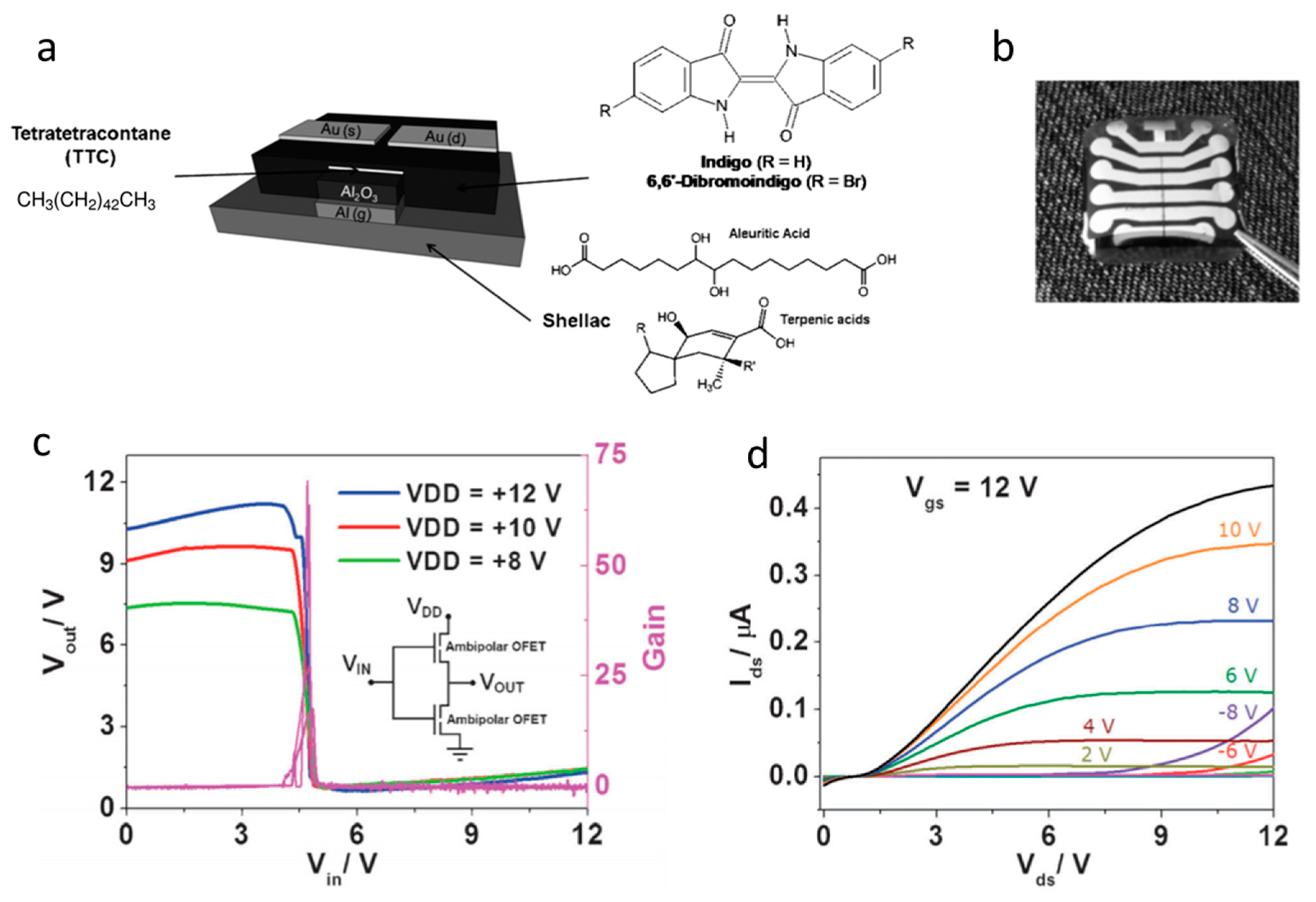
- Głowacki, E.D.; Voss, G.; Leonat, L.; Irimia-Vladu, M.; Bauer, S.; Sariciftci, N.S. Indigo and Tyrian Purple—From Ancient Natural Dyes to Modern Organic Semiconductors. Isr. J. Chem. 2012, 52, 540–551. [Google Scholar] [CrossRef]
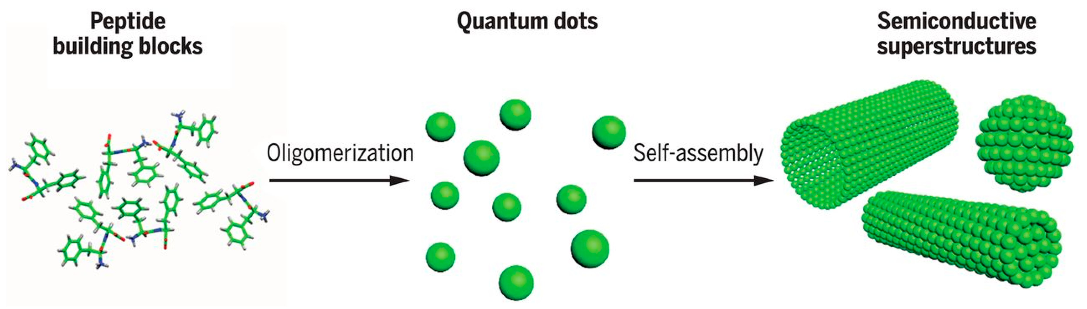
- Tao, K.; Makam, P.; Aizen, R.; Gazit, E. Self-assembling peptide semiconductors. Science 2017, 358, eaam9756. [Google Scholar] [CrossRef] [Green Version]
- Azuri, I.; Adler-Abramovich, L.; Gazit, E.; Hod, O.; Kronik, L. Why are diphenylalanine-based peptide nanostructures so rigid? Insights from first principles calculations. J. Am. Chem. Soc. 2014, 136, 963–969. [Google Scholar] [CrossRef] [PubMed]
- Pinotsi, D.; Grisanti, L.; Mahou, P.; Gebauer, R.; Kaminski, C.F.; Hassanali, A.; Kaminski Schierle, G.S. Proton transfer and structure-specific fluorescence in hydrogen bond-rich protein structures. J. Am. Chem. Soc. 2016, 138, 3046–3057. [Google Scholar] [CrossRef] [Green Version]
- Akdim, B.; Pachter, R.; Naik, R.R. Self-assembled peptide nanotubes as electronic materials: An evaluation from first-principles calculations. Appl. Phys. Lett. 2015, 106, 183707. [Google Scholar] [CrossRef]
- Amit, M.; Cheng, G.; Hamley, I.W.; Ashkenasy, N. Conductance of amyloid β based peptide filaments: Structure-function relations. Soft Matter 2012, 8, 8690–8696. [Google Scholar] [CrossRef]
- Amit, M.; Appel, S.; Cohen, R.; Cheng, G.; Hamley, I.W.; Ashkenasy, N. Hybrid proton and electron transport in peptide fibrils. Adv. Funct. Mater. 2014, 24, 5873–5880. [Google Scholar] [CrossRef]
- Wang, C.H.; Hsieh, C.Y.; Hwang, J.C. Flexible Organic Thin-Film Transistors with Silk Fibroin as the Gate Dielectric. Adv. Mater. 2011, 23, 1630–1634. [Google Scholar] [CrossRef]
- Zang, G.; Hui, H.Y.; Chu†, P.H.; Yuan, Z.; Chang, R.; Risteen, B.; Yang, H.; Reichmanis, E. From Staple Food to Flexible Substrate to Electronics: Rice as a Biocompatible Precursor for Flexible Electronic Components. Chem. Mater. 2016, 28, 8475–8479. [Google Scholar] [CrossRef]
- Valentini, L.; Bittolo Bon, S.; Cardinali, M.; Fortunati, E.; Kenny, J.M. Cellulose nanocrystals thin films as gate dielectric for flexible organic field-effect transistors. Mater. Lett. 2014, 126, 55–58. [Google Scholar] [CrossRef]
- Dai, S.; Chu, Y.; Liu, D.; Cao, F.; Wu, X.; Zhou, J.; Zhou, B.; Chen, Y.; Huang, J. Intrinsically ionic conductive cellulose nanopapers applied as all solid dielectrics for low voltage organic transistors. Nat. Commun. 2018, 9, 2737. [Google Scholar] [CrossRef] [PubMed] [Green Version]
- Seck, M.; Mohammadian, N.; Diallo, A.K.; Faraji, S.; Erouel, M.; Bouguila, N.; Ndiaye, D.; Khirouni, K.; Majewski, L.A. Organic FETs using biodegradable almond gum as gate dielectric: A promising way towards green electronics. Org. Electron. 2020, 83, 105735. [Google Scholar] [CrossRef]
- Shin, E.; Yoo, J.; Yoo, G.; Kim, Y.J.; Kim, Y.S. Eco-friendly cross-linked polymeric dielectric material based on natural tannic acid. Chem. Eng. J. 2019, 358, 170–175. [Google Scholar] [CrossRef]
- Singh, B.; Sariciftci, N.S. Bio-organic-semiconductor-field-effect-transistor based on deoxyribonucleic acid gate dielectric. J. Appl. Phys. 2006, 100, 024514. [Google Scholar] [CrossRef]
- Oppelt, K.; Singh, T.B.; Grote, J.G.; Schwödiauer, R.; Bauer, S.; Piglmayer-Brezina, H.; Bäuerle, D.; Sariciftci, N.S. Organic field-effect transistors and memory elements using deoxyribonucleic acid (DNA) gate dielectric. Org. Electron. 2007, 8, 648. [Google Scholar] [CrossRef]
- Yumusak, C.; Singh, T.B.; Sariciftci, N.S.; Grote, J.G. Bio-organic field effect transistors based on crosslinked deoxyribonucleic acid (DNA) gate dielectric. Appl. Phys. Lett. 2009, 95, 263304. [Google Scholar] [CrossRef]
- Luo, K.; Song, G.; Wang, Y.; Yu, J.; Zhu, J.; Hu, Z. Low-k and Recyclable High-Performance POSS/Polyamide Composites Based on Diels–Alder Reaction. ACS Appl. Polym. Mater. 2019, 1, 944–952. [Google Scholar] [CrossRef]
- Kang, S.K.; Yin, L.; Bettinger, C. The emergence of transient electronic devices. MRS Bull. 2020, 45, 87–95. [Google Scholar] [CrossRef] [Green Version]
- Kumar, S.; Bhatt, K.; Kumar, P.; Sharma, S.; Kumar, A.; Tripathi, C.C. Laser patterned, high-power graphene paper resistor with dual temperature coefficient of resistance. RSC Adv. 2019, 9, 8262–8270. [Google Scholar] [CrossRef] [Green Version]
- Okonkwo, P.C.; Collins, E.; Okonkwo, E. Application of Biopolymer Composites in Super Capacitor. Biopolym. Compos. Electron. 2017, 487–503. [Google Scholar] [CrossRef]
- Lim, C.; Teoh, K.H.; Liew, C.W.; Ramesh, S. Electric double layer capacitor based on activated carbon electrode and biodegradable composite polymer electrolyte. Ionics 2014, 20, 251–258. [Google Scholar] [CrossRef]
- Lee, G.; Kang, S.K.; Won, S.M.; Gutruf, P.; Jeong, Y.R.; Koo, J.; Lee, S.S.; Rogers, J.A.; Ha, J.S. Fully Biodegradable Microsupercapacitor for Power Storage in Transient Electronics. Adv. Energy Mater. 2017, 7, 1700157. [Google Scholar] [CrossRef]
- Yang, Q.; Huang, Z.; Li, X.; Liu, Z.; Li, H.; Liang, G.; Wang, D.; Huang, Q.; Zhang, S.; Chen, S.; et al. A Wholly Degradable, Rechargeable Zn–Ti3C2 MXene Capacitor with Superior Anti-Self-Discharge Function. ACS Nano 2019, 13, 8275–8283. [Google Scholar] [CrossRef]
- Hamsan, M.H.; Shukur, M.F.; Kadir, M.F.Z. NH4NO3 as charge carrier contributor in glycerolized potato starch-methyl cellulose blend-based polymer electrolyte and the application in electrochemical double-layer capacitor. Ionics 2017, 23, 3429–3453. [Google Scholar] [CrossRef]
- Kasturi, P.R.; Ramasamy, H.; Meyrick, D.; Lee, Y.S.; Selvan, R.K. Preparation of starch-based porous carbon electrode and biopolymer electrolyte for all solid-state electric double layer capacitor. J. Colloid Interface Sci. 2019, 554, 142–156. [Google Scholar] [CrossRef] [PubMed]
- Nowacki, K.; Galiński, M.; Stępniak, I. Synthesis and characterization of modified chitosan membranes for applications in electrochemical capacitor. Electrochim. Acta 2019, 134632. [Google Scholar] [CrossRef]
- Avila-Niño, J.A.; Vilchis, S.; Araujo, E. Flexible and transparent capacitors based on gel-type natural polymers. J. Appl. Polym. Sci. 2020, e49028. [Google Scholar] [CrossRef]
- Menzel, J.; Frąckowiak, E.; Fic, K. Agar-based aqueous electrolytes for electrochemical capacitors with reduced self-discharge. Electrochim. Acta 2020, 332, 135435. [Google Scholar] [CrossRef]
- Li, H.; Zhao, C.C.; Wang, X.X.; Meng, J.P.; Zou, Y.; Noreen, S.; Zhao, L.M.; Liu, Z.; Ouyang, H.; Tan, P.C.; et al. Fully Bioabsorbable Capacitor as an Energy Storage Unit for Implantable Medical Electronics. Adv. Sci. 2019, 6, 1801625. [Google Scholar] [CrossRef] [Green Version]
- Guo, J.; Liu, J.; Yang, B.; Zhan, G.; Tang, L.; Tian, H.; Kang, X.; Peng, H.; Chen, X.; Yang, C. Biodegradable Junctionless Transistors With Extremely Simple Structure. IEEE Electron Device Lett. 2015, 36, 908–910. [Google Scholar] [CrossRef]
- Rullyani, C.; Ramesh, M.; Sung, C.F.; Lin, H.C.; Chu, C.W. Natural polymers for disposable organic thin film transistors. Org. Electron. 2018, 54, 154–160. [Google Scholar] [CrossRef]
- Jo, Y.J.; Kim, H.; Ok, J.; Shin, Y.J.; Shin, J.H.; Kim, T.H.; Jung, Y.; Kim, T.I. Biodegradable Organic Transistors: Biocompatible and Biodegradable Organic Transistors Using a Solid-State Electrolyte Incorporated with Choline-Based Ionic Liquid and Polysaccharide. Adv. Funct. Mater. 2020, 30, 2070190. [Google Scholar] [CrossRef]
- Yang, Y.H.; Li, J.; Chen, Q.; Zhou, Y.H.; Zhu, W.Q.; Zhang, J.H. Double-gate InZnO synaptic transistor with aqueous-solution-processed wheat flour electrolyte. Org. Electron. 2020, 77, 105518. [Google Scholar] [CrossRef]
- Pettersson, F.; Österbacka, R.; Koskela, J.; Kilpelä, A.; Remonen, T.; Zhang, Y.; Inkinen, S.; Wilén, C.E.; Bollström, R.; Toivakka, M.; et al. Ion-modulated transistors on paper using phase-separated semiconductor/insulator blends. MRS Commun. 2014, 4, 51–55. [Google Scholar] [CrossRef]
- Kim, S.; Ren, Y.; Lee, H.; Rida, A.; Nikolaou, S.; Tentzeris, M.M. Monopole Antenna With Inkjet-Printed EBG Array on Paper Substrate for Wearable Applications. IEEE Antennas Wirel. Propag. Lett. 2012, 11, 663–666. [Google Scholar] [CrossRef] [Green Version]
- Akbari, M.; Khan, M.W.A.; Hasani, M.; Björninen, T.; Sydänheimo, L.; Ukkonen, L. Fabrication and Characterization of Graphene Antenna for Low-Cost and Environmentally Friendly RFID Tags. IEEE Antennas Wirel. Propag. Lett. 2016, 15, 1569–1572. [Google Scholar] [CrossRef]
- Kanaparthi, S.; Sekhar, V.R.; Badhulika, S. Flexible, eco-friendly and highly sensitive paper antenna based electromechanical sensor for wireless human motion detection and structural health monitoring. Extrem. Mech. Lett. 2016, 9, 324–330. [Google Scholar] [CrossRef]
- Teng, L.; Ye, S.C.; Handschuh-Wang, S.; Zhou, X.H.; Gan, T.S.; Zhou, X.C. Liquid Metal-Based Transient Circuits for Flexible and Recyclable Electronics. Adv. Funct. Mater. 2019, 29, 1808739. [Google Scholar] [CrossRef]
- Katz, E.; Bückmann, A.F.; Willner, I. Self-Powered Enzyme-Based Biosensors. J. Am. Chem. Soc. 2001, 123, 10752–10753. [Google Scholar] [CrossRef]
- Hao, S.; Sun, X.; Zhang, H.; Zhai, J.; Dong, S. Recent development of biofuel cell based self-powered biosensors. J. Mater. Chem. B 2020, 8, 3393–3407. [Google Scholar] [CrossRef] [PubMed]
- Mano, N.; de Poulpiquet, A. O2 reduction in enzymatic biofuel cells. Chem. Rev. 2018, 118, 2392–2468. [Google Scholar] [CrossRef] [PubMed] [Green Version]
- Żelechowska, K.; Stolarczyk, K.; Łyp, D.; Rogalski, J.; Roberts, K.P.; Bilewicz, R.; Biernat, J.F. Aryl and N-arylamide carbon nanotubes for electrical coupling of laccase to electrodes in biofuel cells and biobatteries. Biocybern. Biomed. Eng. 2013, 3, 235–245. [Google Scholar] [CrossRef]
- Stolarczyk, K.; Kizling, M.; Majdecka, D.; Żelechowsk, K.; Biernat, J.F.; Rogalski, J.; Bilewicz, R. Biobatteries and biofuel cells with biphenylated carbon nanotubes. J. Power Sources 2014, 249, 263–269. [Google Scholar] [CrossRef]
- Kerr, J.; Minteer, S.D. Development of lipoxygenase bioanodes for biofuel cells. Abs. Pap. Am. Chem. Soc. 2006, 231, 352. [Google Scholar]
- Moehlenbrock, M.J.; Minteer, S.D. Extended lifetime biofuel cells. Chem. Soc. Rev. 2008, 37, 1188–1196. [Google Scholar] [CrossRef]
- Filip, J.; Monosik, R.; Tkac, J. Poly(lactic acid)-based Nanocomposite for Construction of Efficient Bilirubin Oxidase-Based Biocathodes and Stable Biofuel Cells. Int. J. Electrochem. Sci. 2014, 9, 2491–2506. [Google Scholar]
- Jenkins, P.; Tuurala, S.; Vaari, A.; Valkiainen, M.; Smolander, M.; Leech, D. A mediated glucose/oxygen enzymatic fuel cell based on printed carbon inks containing aldose dehydrogenase and laccase as anode and cathode. Enzyme Microb. Technol. 2012, 50, 181–187. [Google Scholar] [CrossRef]
- Shitanda, I.; Kato, S.; Hoshi, Y.; Itagaki, M.; Tsujimura, S. Electrodes are screen-printed on both side of a Japanese paper. Chem. Commun. 2013, 49, 11110–11112. [Google Scholar] [CrossRef]
- Wu, X.E.; Guo, Y.Z.; Chen, M.Y.; Chen, X.D. Fabrication of flexible and disposable enzymatic biofuel cells. Electroanalysis 2016, 28, 1188–1200. [Google Scholar] [CrossRef]
- Ciniciato, G.; Lau, C.; Cochrane, A.; Sibbett, S.S.; Gonzalez, E.R.; Atanassov, P. Development of paper based electrodes: From air-breathing to paintable enzymatic cathodes. Electrochim. Acta 2012, 82, 208–213. [Google Scholar] [CrossRef]
- Desmet, C.; Marquette, C.A.; Blum, L.J.; Doumèche, B. Paper electrodes for bioelectrochemistry: Biosensors and biofuel cells. Biosens. Bioelectron. 2016, 76, 145–163. [Google Scholar] [CrossRef] [PubMed]
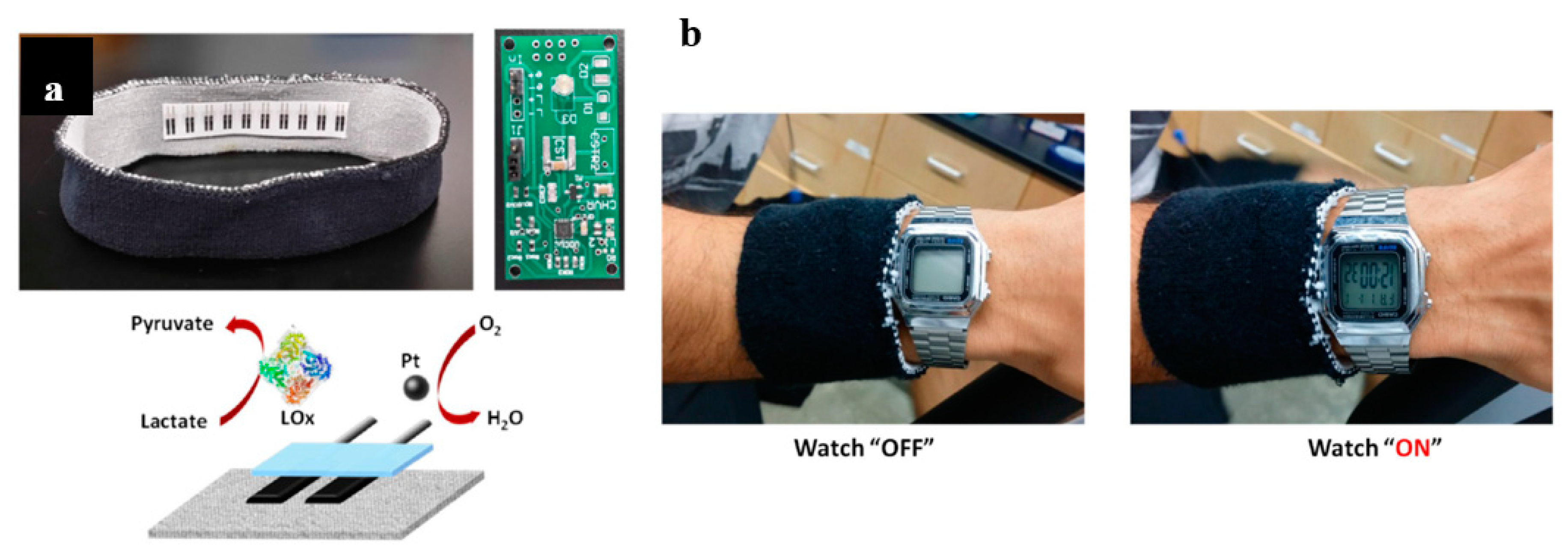
- Bandodkar, A.J.; Wang, J. Wearable Biofuel Cells: A Review. Electroanalysis 2016, 28, 1188–1200. [Google Scholar] [CrossRef]
- Jia, W.; Wang, X.; Imani, S.; Bandodkar, A.J.; Ramirez, J.; Mercier, P.P.; Wang, J. Wearable textile biofuel cells for powering electronics. J. Mater. Chem. A 2014, 2, 18184–18189. [Google Scholar] [CrossRef]
- Gross, A.J.; Holzinger, M.; Cosnier, S. Buckypaper bioelectrodes: Emerging materials for implantable and wearable biofuel cells. Energy Environ. Sci. 2018, 11, 1670–1687. [Google Scholar] [CrossRef]
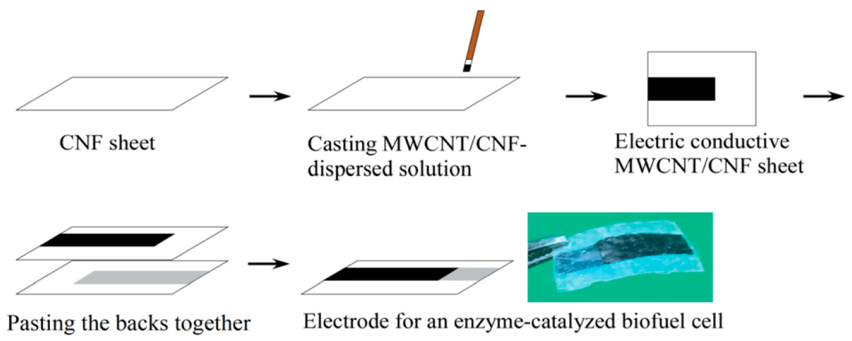
- Tominaga, M.; Kuwaharaa, K.; Tsushida, M.; Shida, K. Cellulose nanofiber-based electrode as a component of an enzyme-catalyzed biofuel cell. RSC Adv. 2020, 10, 22120–22125. [Google Scholar] [CrossRef]
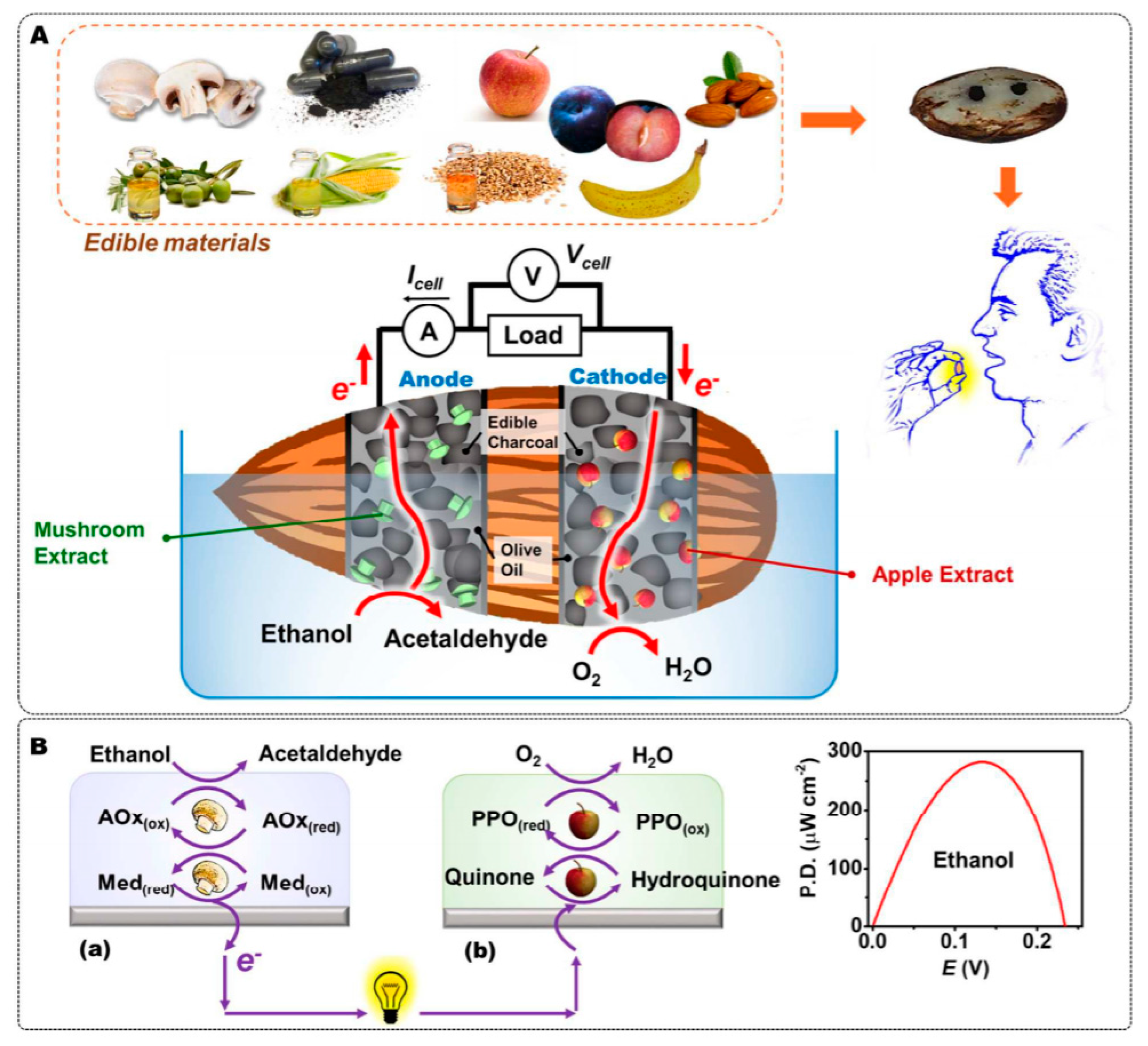
- Jeerapan, I.; Ciui, B.; Martin, I.; Cristea, C.; Sandulescu, R.; Wang, J. Fully edible biofuel cells. J. Mater. Chem. B 2018, 6, 3571–3578. [Google Scholar] [CrossRef]
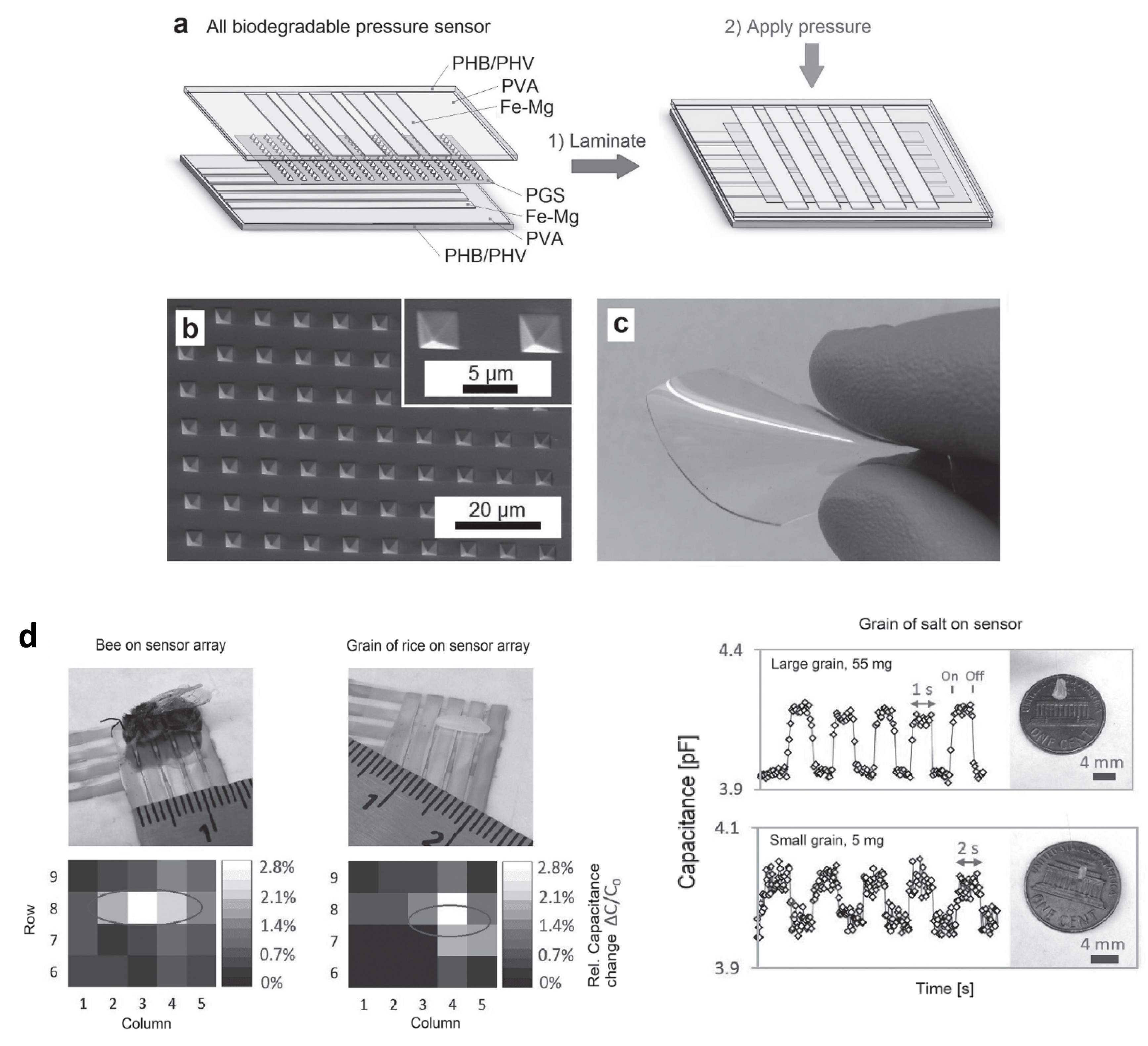
- Annese, V.F.; De Venuto, D.; Martin, C.; Cumming, D.R.S. Biodegradable pressure sensor for health-care. In Proceedings of the IEEE International Conference on Electronics, Circuits and Systems 2014, Marseille, France, 7–10 December 2014; pp. 598–601. [Google Scholar] [CrossRef]
- Luo, M.; Martinez, A.W.; Song, C.; Herrault, F.; Allen, M.G. A Microfabricated Wireless RF Pressure Sensor Made Completely of Biodegradable Materials. J. Microelectromech. Syst. 2014, 23, 4–13. [Google Scholar] [CrossRef]
- Boutry, C.M.; Nguyen, A.; Lawal, Q.O.; Chortos, A.; Rondeau-Gagné, S.; Bao, Z. A Sensitive and Biodegradable Pressure Sensor Array for Cardiovascular Monitoring. Adv. Mater. 2015, 27, 6954–6961. [Google Scholar] [CrossRef]
- Boutry, C.M.; Beker, L.; Kaizawa, Y.; Vassos, C.; Tran, H.; Hinckley, A.C.; Pfattner, R.; Niu, S.; Li, J.; Claverie, J.; et al. Biodegradable and flexible arterial-pulse sensor for the wireless monitoring of blood flow. Nat. Biomed. Eng. 2019, 3, 47–57. [Google Scholar] [CrossRef]
- Hosseini, E.S.; Manjakkal, L.; Shakthivel, D.; Dahiya, R. Glycine–Chitosan-Based Flexible Biodegradable Piezoelectric Pressure Sensor. ACS Appl. Mater. Interfaces 2020, 12, 9008–9016. [Google Scholar] [CrossRef] [PubMed] [Green Version]
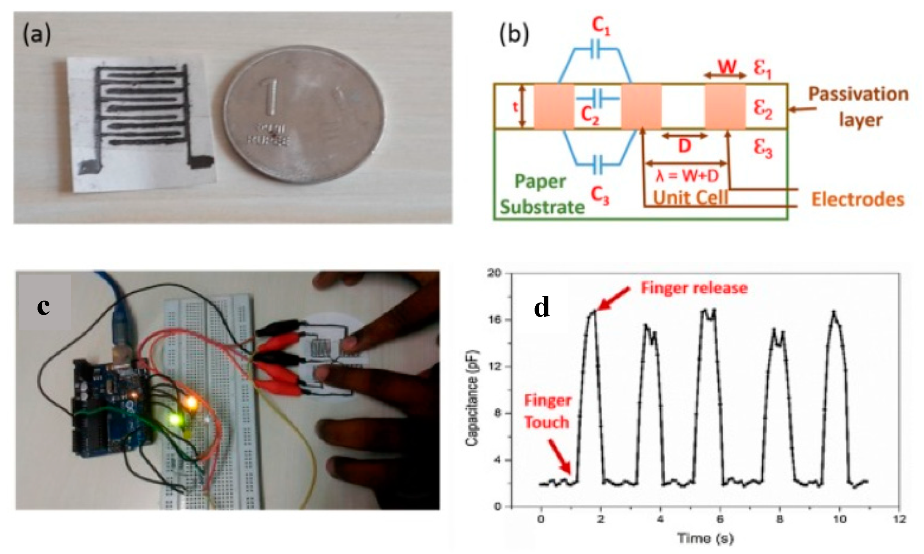
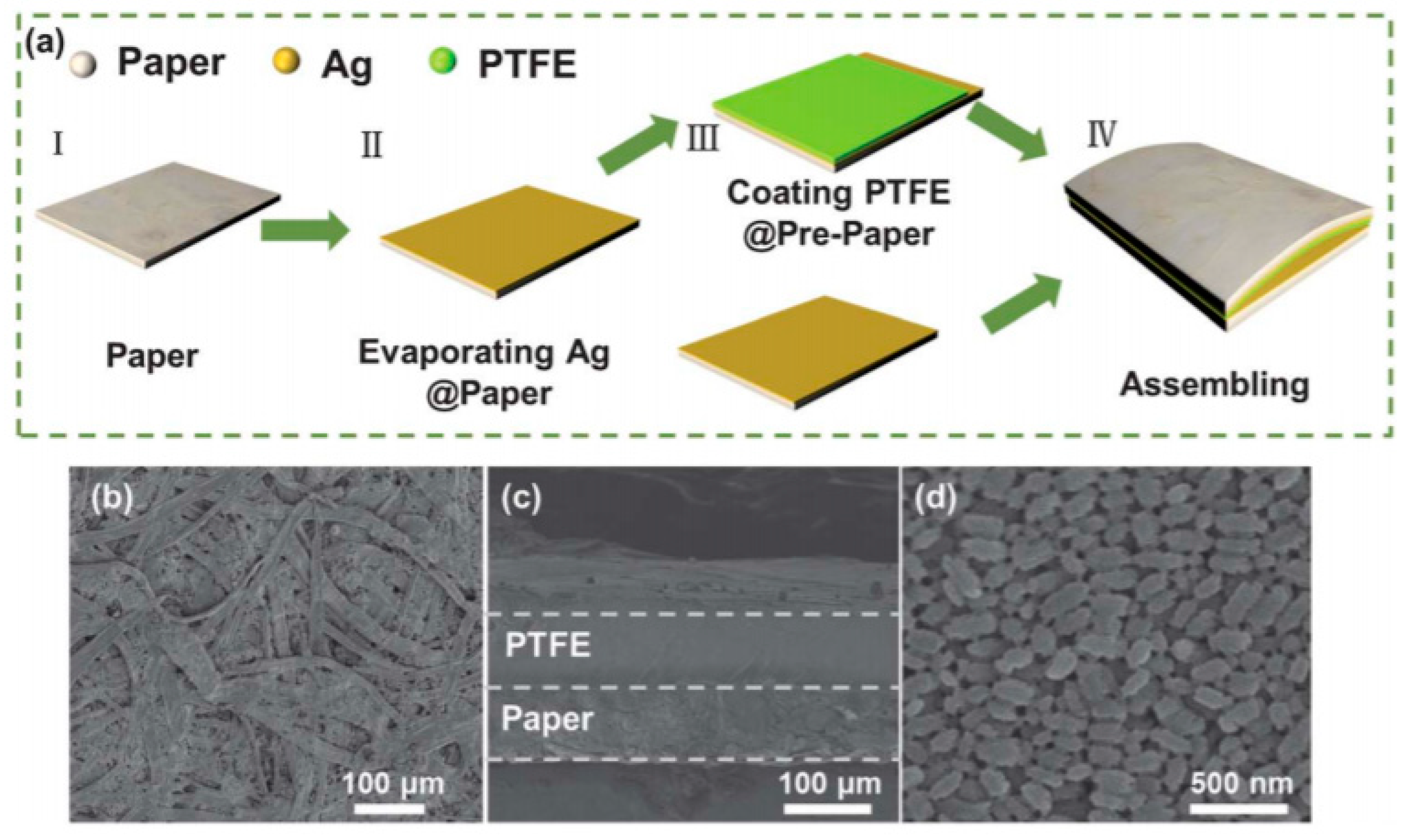
- Kanaparthi, S.; Badhulika, S. Low cost, flexible and biodegradable touch sensor fabricated by solvent-free processing of graphite on cellulose paper. Sens. Actuators B Chem. 2017, 242, 857–864. [Google Scholar] [CrossRef]
- Zhong, Q.; Zhong, J.; Hu, B.; Hu, Q.; Zhou, J.; Wang, Z.L. A paper-based nanogenerator as a power source and active sensor. Energy Environ. Sci. 2013, 6, 1779. [Google Scholar] [CrossRef]
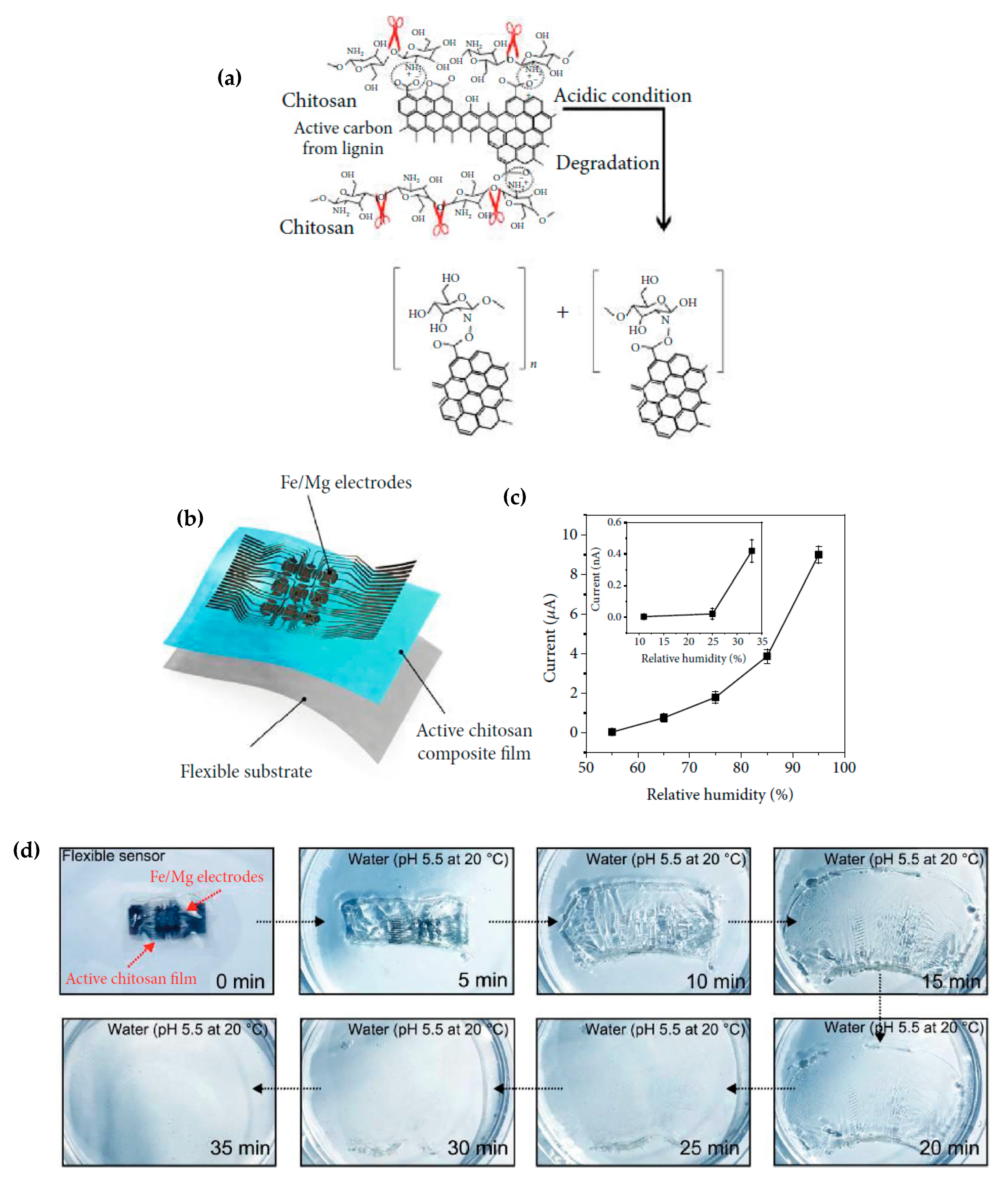
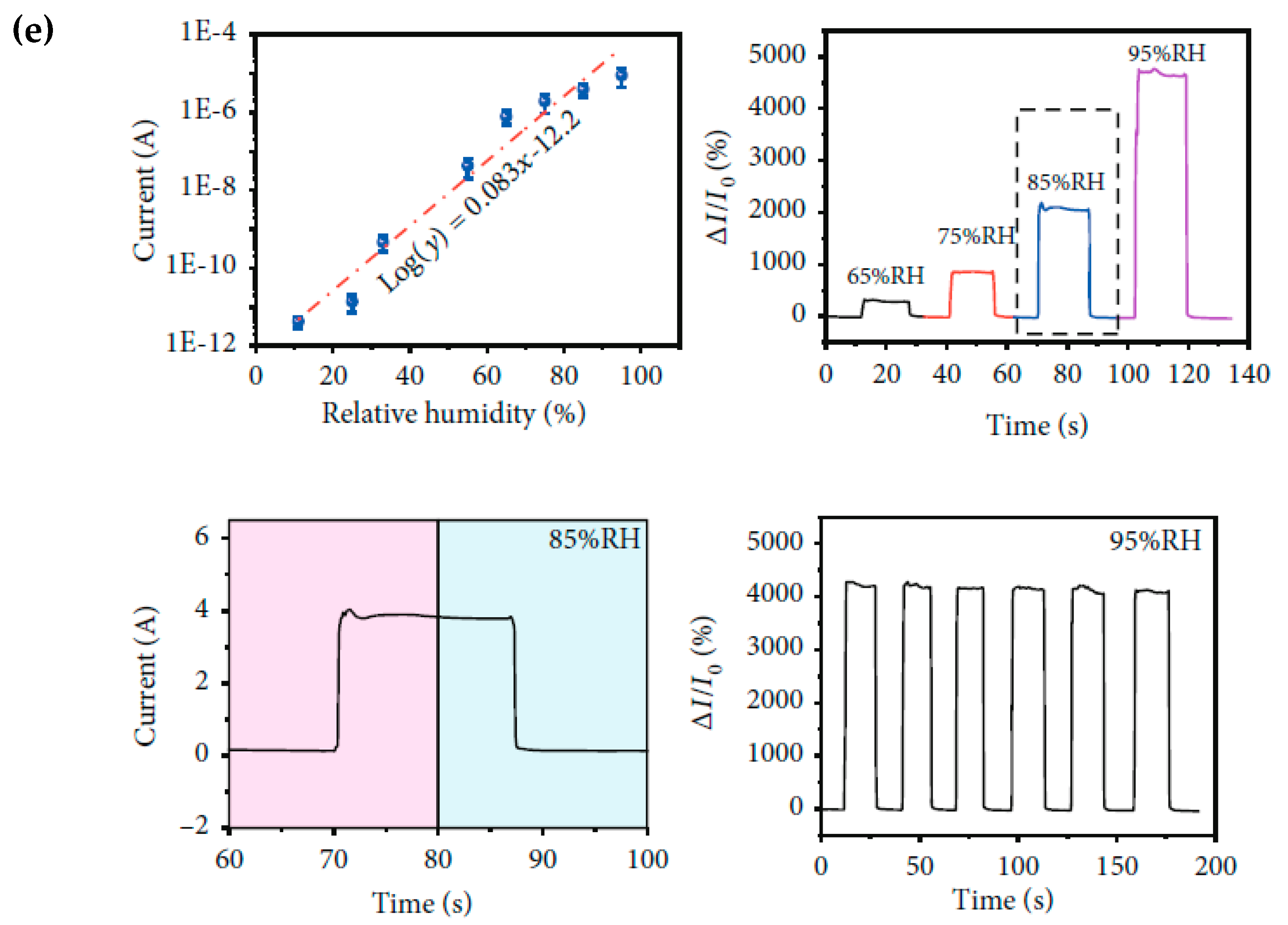
- Wang, L.; Lou, Z.; Wang, K.; Zhao, S.; Yu, P.; Wei, W.; Wang, D.; Han, W.; Jiang, K.; Shen, G. Biocompatible and Biodegradable Functional Polysaccharides for Flexible Humidity Sensors. Research 2020, 8716847. [Google Scholar] [CrossRef] [PubMed] [Green Version]
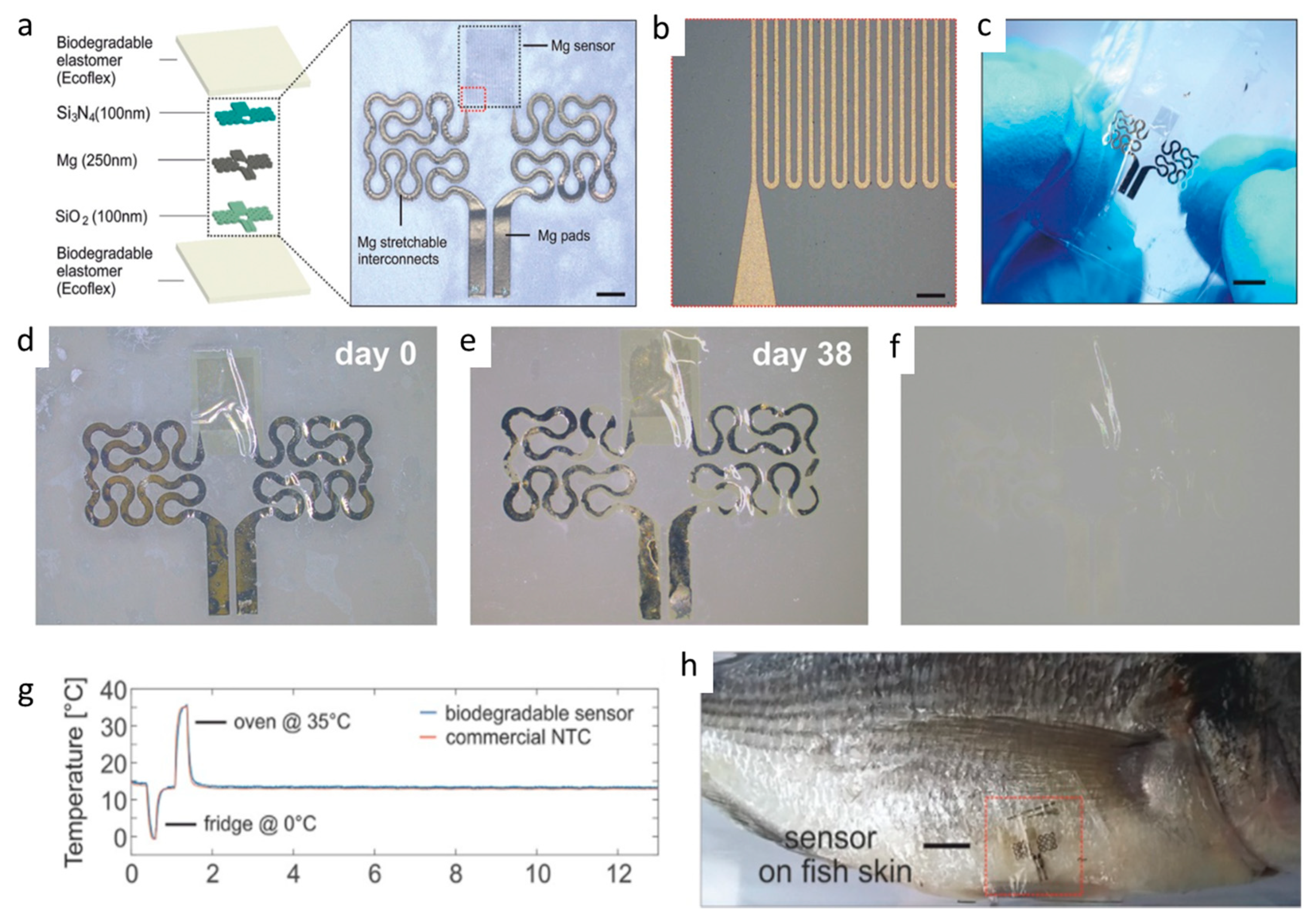
- Salvatore, G.A.; Sülzle, J.; Dalla Valle, F.; Cantarella, G.; Robotti, F.; Jokic, P.; Knobelspies, S.; Daus, A.; Büthe, L.; Petti, L.; et al. Biodegradable and highly deformable temperature sensors for the internet of things. Adv. Funct. Mater. 2017, 27, 1702390. [Google Scholar] [CrossRef]
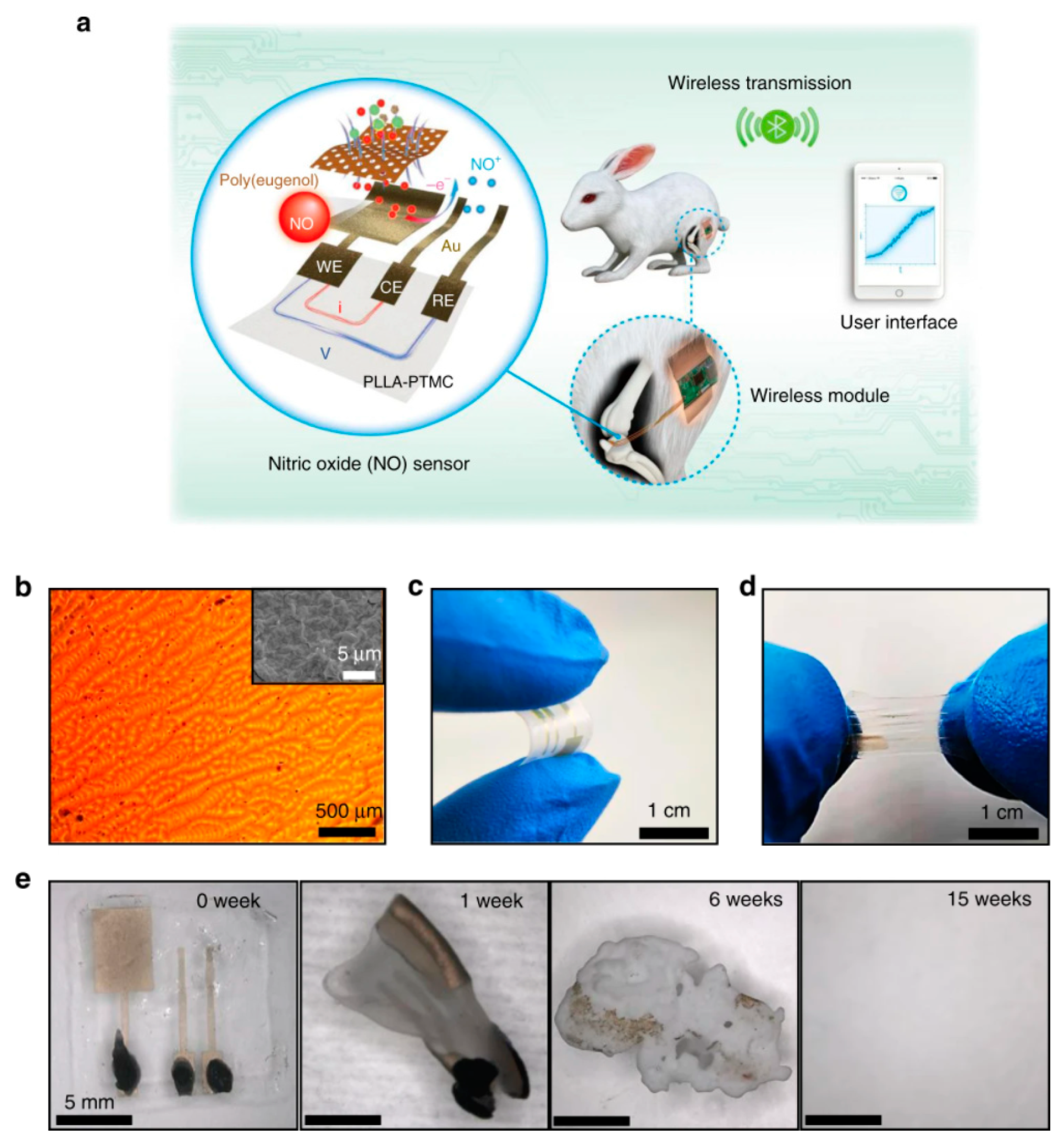
- Li, R.; Qi, H.; Ma, Y.; Deng, Y.; Liu, S.; Jie, Y.; Jing, J.; He, J.; Zhang, X.; Wheatley, L.; et al. A flexible and physically transient electrochemical sensor for real-time wireless nitric oxide monitoring. Nat. Commun. 2020, 11, 3207. [Google Scholar] [CrossRef] [PubMed]
- Mattana, G.; Loi, A.; Woytasik, M.; Barbaro, M.; Noël, V.; Piro, B. Inkjet-Printing: A New Fabrication Technology for Organic Transistors. Adv. Mater. Technol. 2017, 2, 1700063. [Google Scholar] [CrossRef]
- Ferreira Cruz, S.M.; Rocha, L.A.; Viana, J.C. Printing Technologies on Flexible Substrates for Printed Electronics. In Flexible Electronics; IntechOpen: London, UK, 2018. [Google Scholar] [CrossRef] [Green Version]
- Huang, Q.; Zhu, Y. Printing Conductive Nanomaterials for Flexible and Stretchable Electronics: A Review of Materials, Processes, and Applications. Adv. Mater. Technol. 2019, 4, 1800546. [Google Scholar] [CrossRef]
- Khan, S.; Lorenzelli, L.; Dahiya, R.S. Technologies for Printing Sensors and Electronics Over Large Flexible Substrates: A Review. IEEE Sens. J. 2015, 15, 3164–3185. [Google Scholar] [CrossRef]
- Kanaparthi, S. Solvent-Free Fabrication of Eco-Friendly All-Carbon Flexible Paper Electronics. Master’s Thesis, Indian Institute of Technology Hyderabad, Kandi, Telangana, India, 2016. Available online: http://raiith.iith.ac.in/id/eprint/2606 (accessed on 3 August 2020).
- Peng, B.; Chan, P.K.L. Flexible organic transistors on standard printing paper and memory properties induced by floated gate electrode. Org. Electron. 2014, 15, 203–210. [Google Scholar] [CrossRef]
- Bihar, E.; Wustoni, S.; Pappa, A.M.; Salama, K.N.; Baran, D.; Inal, S. A fully inkjet-printed disposable glucose sensor on paper. NPJ Flex. Electron. 2018, 2, 30. [Google Scholar] [CrossRef] [Green Version]
- Bedük, T.; Bihar, E.; Surya, S.G.; Robles, A.N.C.; Inal, S.; Salama, K.N. A paper-based inkjet-printed PEDOT:PSS/ZnO sol-gel hydrazine sensor. Sens. Actuators B Chem. 2019, 127539. [Google Scholar] [CrossRef]
- Serpelloni, M.; Cantù, E.; Borghetti, M.; Sardini, E. Printed Smart Devices on Cellulose-Based Materials by means of Aerosol-Jet Printing and Photonic Curing. Sensors 2020, 20, 841. [Google Scholar] [CrossRef] [PubMed] [Green Version]
- Wie, D.S.; Zhang, Y.; Kim, M.K.; Kim, B.; Park, S.; Kim, Y.J.; Irazoqui, P.P.; Zheng, X.; Xu, B.; Lee, C.H. Wafer-recyclable, environment-friendly transfer printing for large-scale thin-film nanoelectronics. Proc. Natl. Acad. Sci. USA 2018, 115, E7236–E7244. [Google Scholar] [CrossRef] [PubMed]


| Acronyms | Definitions | Acronyms | Definitions |
|---|---|---|---|
| AFM | Atomic Force Microscopy | RIE | Reactive-Ion Etching |
| BFC | Biofuel Cell | PBS | Phosphate Buffer Saline |
| CCR | Carbon Composition Resistance | PCB | Printed Circuit Board |
| CMOS | Complementary Metal Oxide Semiconductor | PDMS | Poly(DimethylSiloxane) |
| DNTT | DiNaphtho[2,3-b:2′,3′-f]Thieno[3,2-b]Thiophene | PEDOT | Poly(3,4-ethylenedioxythiophene) |
| DPPDTT | Poly(3,6-di (2-thien-5-yl)-2,5-di (2-octyldodecyl)-Pyrrolo [3,4-c] Pyrrole-1,4-Dione)Thieno [3,2-b] Thiophene) | PECVD | Plasma-Enhanced Chemical Vapor Deposition |
| EDLC | Electrochemical Double Layer Capacitor | P3HT | Poly(3-hexylthiophene) |
| EGT | Electrolyte-Gated Transistor | PI | Poly(imide) |
| FET | Field-Effect Transistor | PMMA | Poly(MethylMethAcrylate) |
| HBT | Heterojunction Bipolar Transistors | PSS | Poly(styrene sulfonate) |
| IoT | Internet of Things | PTCDI-C8 | N,N′-Dioctyl-3,4,9,10-perylenedicarboximide |
| LED | Light Emitting Diode | PTFE | PolyTetraFluoroEthylene |
| MOSFET | Metal Oxide Silicon Field-Effect Transistor | RRC | Relative Resistance Changes |
| NTA | NanoTube Array | SEM | Scanning Electron Microscopy |
| NTC | Negative Temperature Coefficient | TCR | Temperature Coefficient Resistance |
| OFET | Organic Field-Effect Transistor |
| Name | Structure | Full Name |
|---|---|---|
| Ag | - | Silver |
| AgNW | - | Silver NanoWire |
| Al | - | Aluminum |
| CHE CKF CNF |  | Cellulose-based Hydrogel Electrolytes Cellulose/KOH Film Cellulose NanoFibril |
| DNA | - | DesoxyriboNucleic Acid |
| Fe | - | Iron |
| FF |  | Diphenylalanine |
| FW |  | Phenylalanine-Triptophan |
| GO | - | Graphene Oxide |
| IGZO | - | Indium-Gallium-Zinc Oxide |
| Indigo |  | Indigo |
| IZO | - | Indium-Zinc Oxide |
| LCF |  | Lignin-derived Carbonized Nanofibers |
| Mg | - | Magnesium |
 | ||
| PGS | W with R = H | Poly(Glycerol Sebacate) |
| PHB |  | Poly(HydroxyButyrate) |
| PHV |  | Poly(HydroxyValerate) |
| PLLA PDLA PLA |  | Poly(L-Lactic Acid) Poly(D-Lactic Acid) Poly(Lactic acid) |
| PLGA |  | Poly(lactic-co-glycolic acid) |
| POMaC |  | Poly(Octamethylene Maleate Anhydride Citrate) |
| POSS |  | Polyhedral Oligomeric SilSesquioxane |
| PTMC |  | Poly(TriMethylene Carbonate) |
| PVA |  | Poly(VinylAlcohol) |
| RF | - | Rice Film |
| rGO | - | Reduced Graphene Oxide |
| SA |  | Sodium Alginate |
| Si | - | Silicon |
| SOG | - | Silica spin-On-Glass |
| TTC |  | TetraTretraContane |
| Zn | - | Zinc |
Publisher’s Note: MDPI stays neutral with regard to jurisdictional claims in published maps and institutional affiliations. |
© 2020 by the authors. Licensee MDPI, Basel, Switzerland. This article is an open access article distributed under the terms and conditions of the Creative Commons Attribution (CC BY) license (http://creativecommons.org/licenses/by/4.0/).
Share and Cite
Piro, B.; Tran, H.V.; Thu, V.T. Sensors Made of Natural Renewable Materials: Efficiency, Recyclability or Biodegradability—The Green Electronics. Sensors 2020, 20, 5898. https://doi.org/10.3390/s20205898
Piro B, Tran HV, Thu VT. Sensors Made of Natural Renewable Materials: Efficiency, Recyclability or Biodegradability—The Green Electronics. Sensors. 2020; 20(20):5898. https://doi.org/10.3390/s20205898
Chicago/Turabian StylePiro, Benoît, Hoang Vinh Tran, and Vu Thi Thu. 2020. "Sensors Made of Natural Renewable Materials: Efficiency, Recyclability or Biodegradability—The Green Electronics" Sensors 20, no. 20: 5898. https://doi.org/10.3390/s20205898