Fabrication of Ultraviolet Photodetectors Based on Fe-Doped ZnO Nanorod Structures


Abstract
:1. Introduction
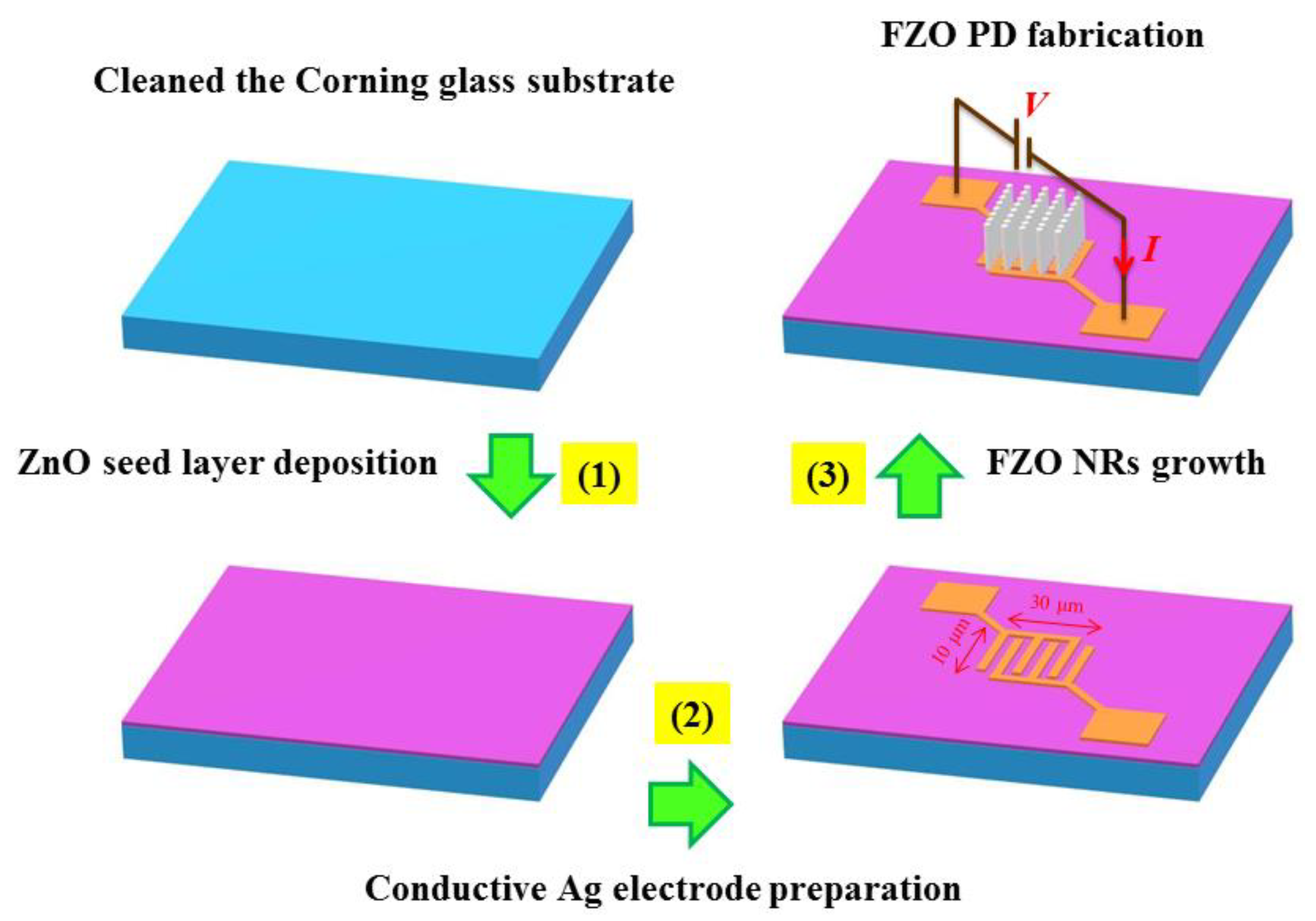
2. Experimental
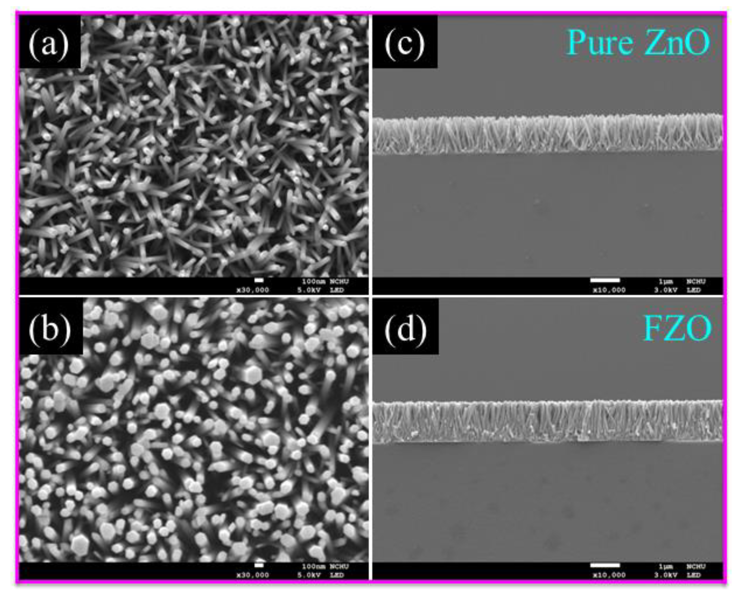
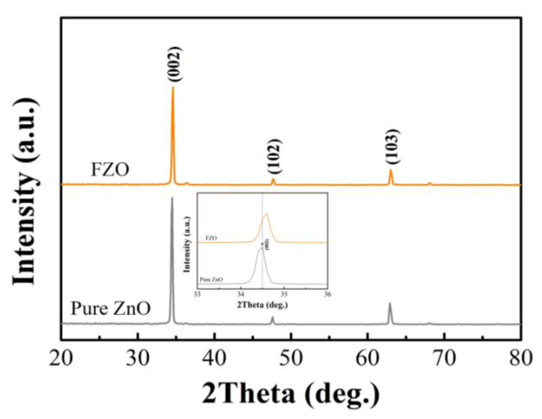
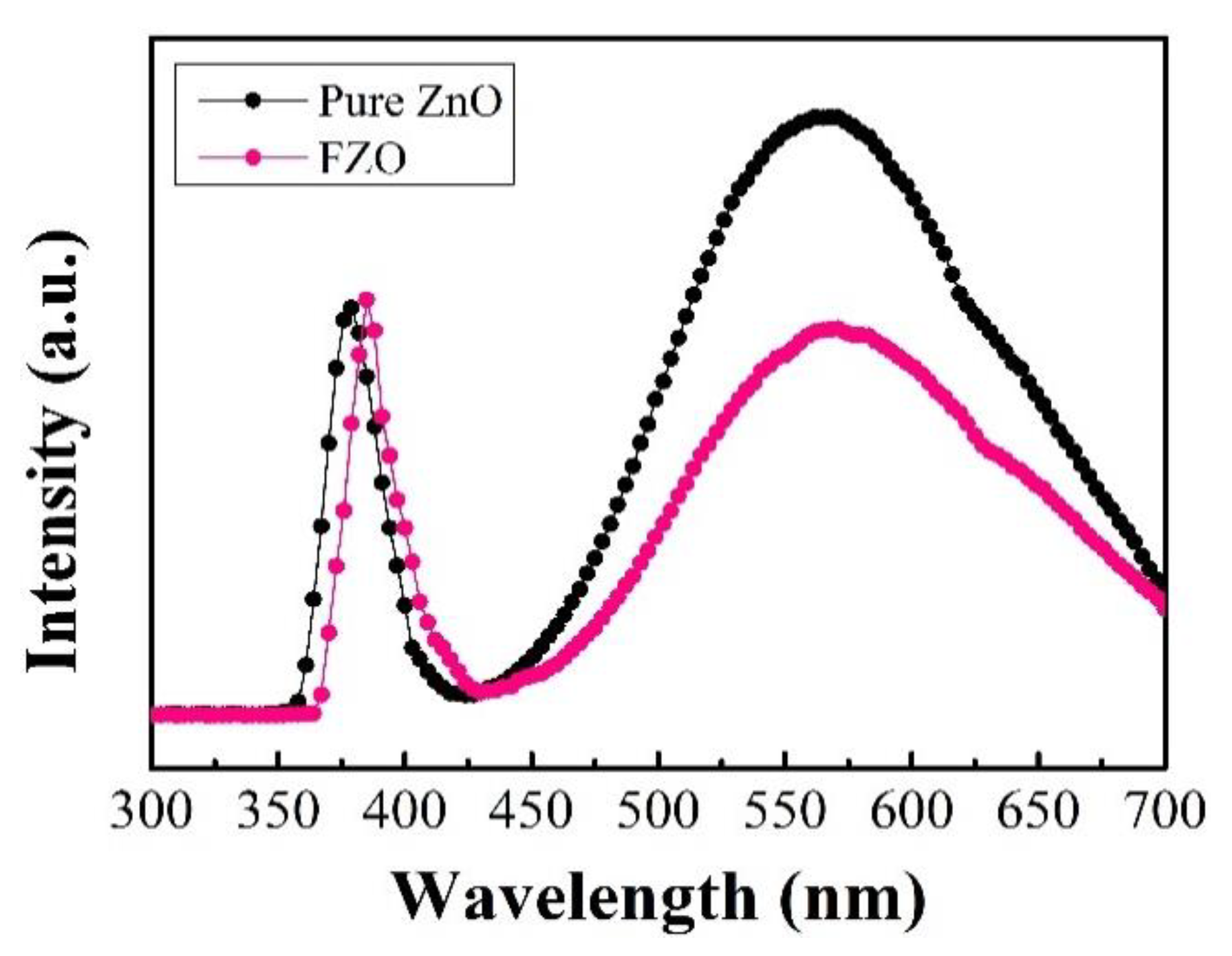
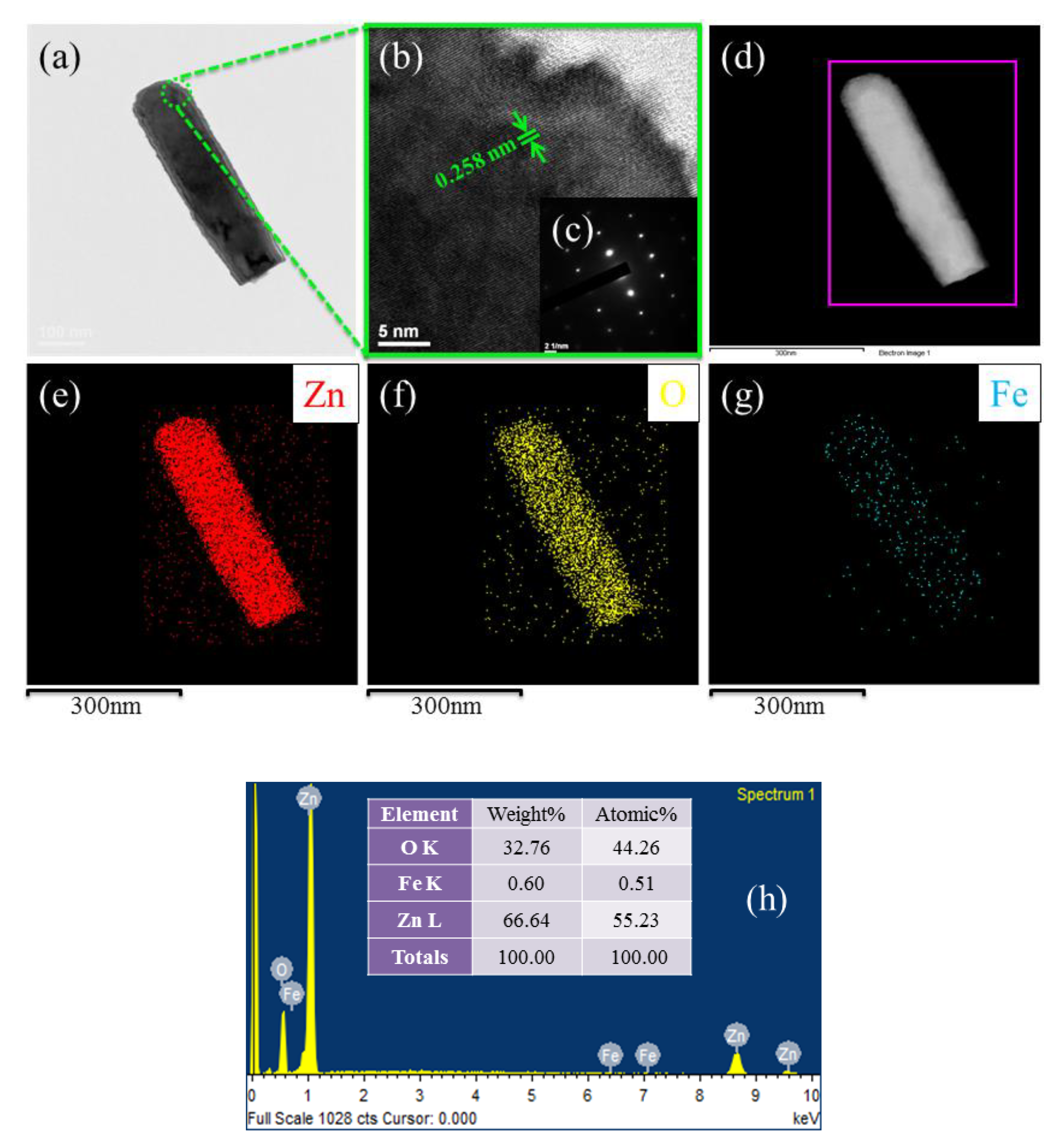
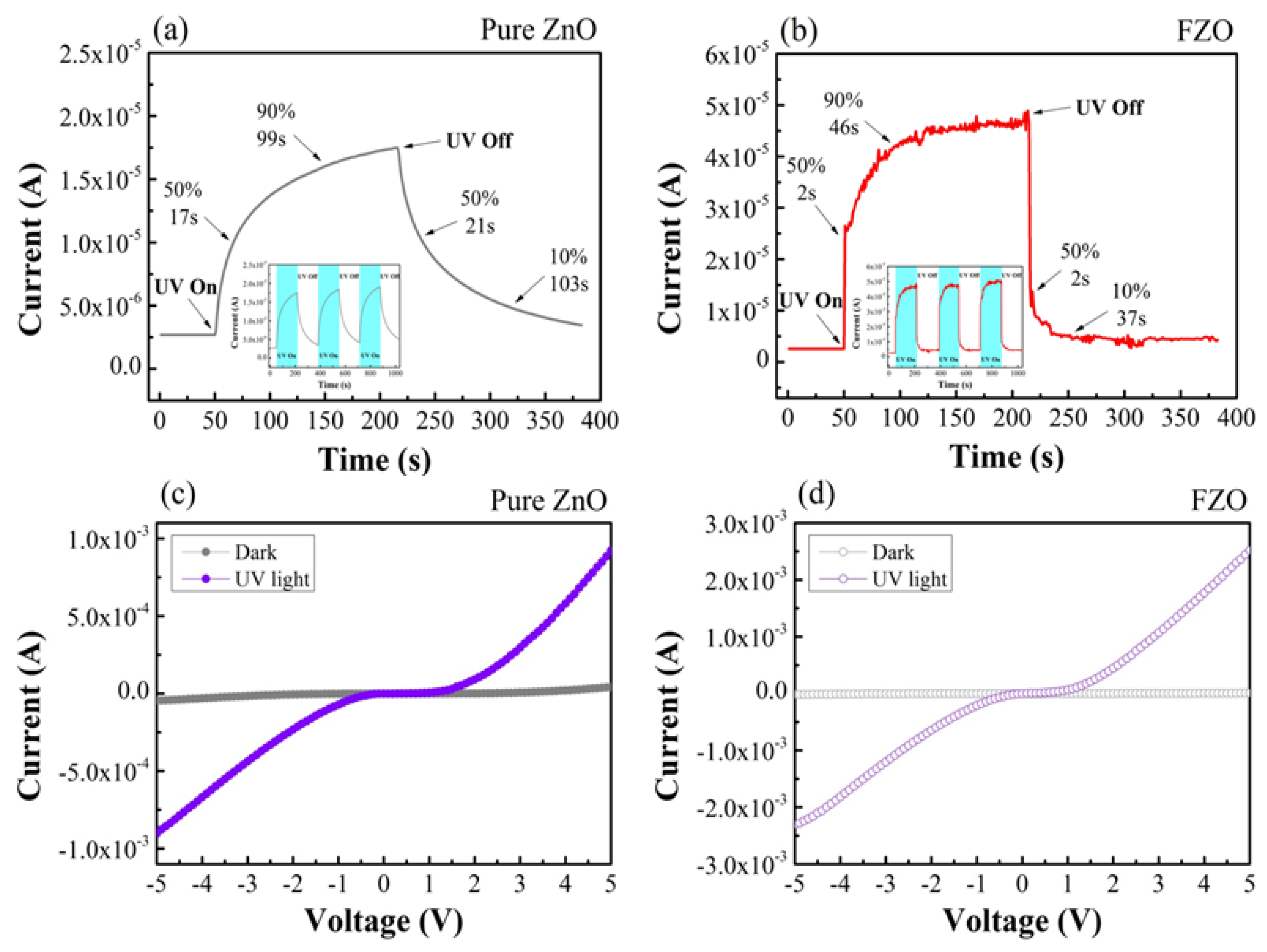
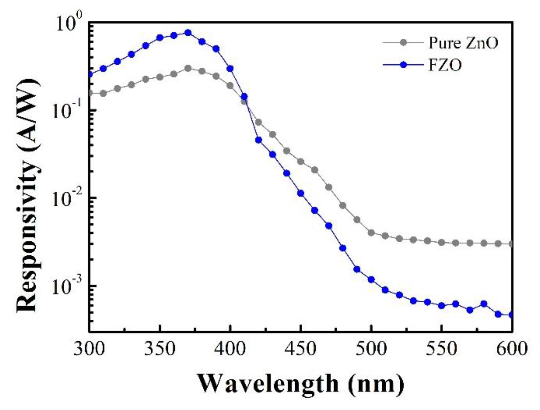
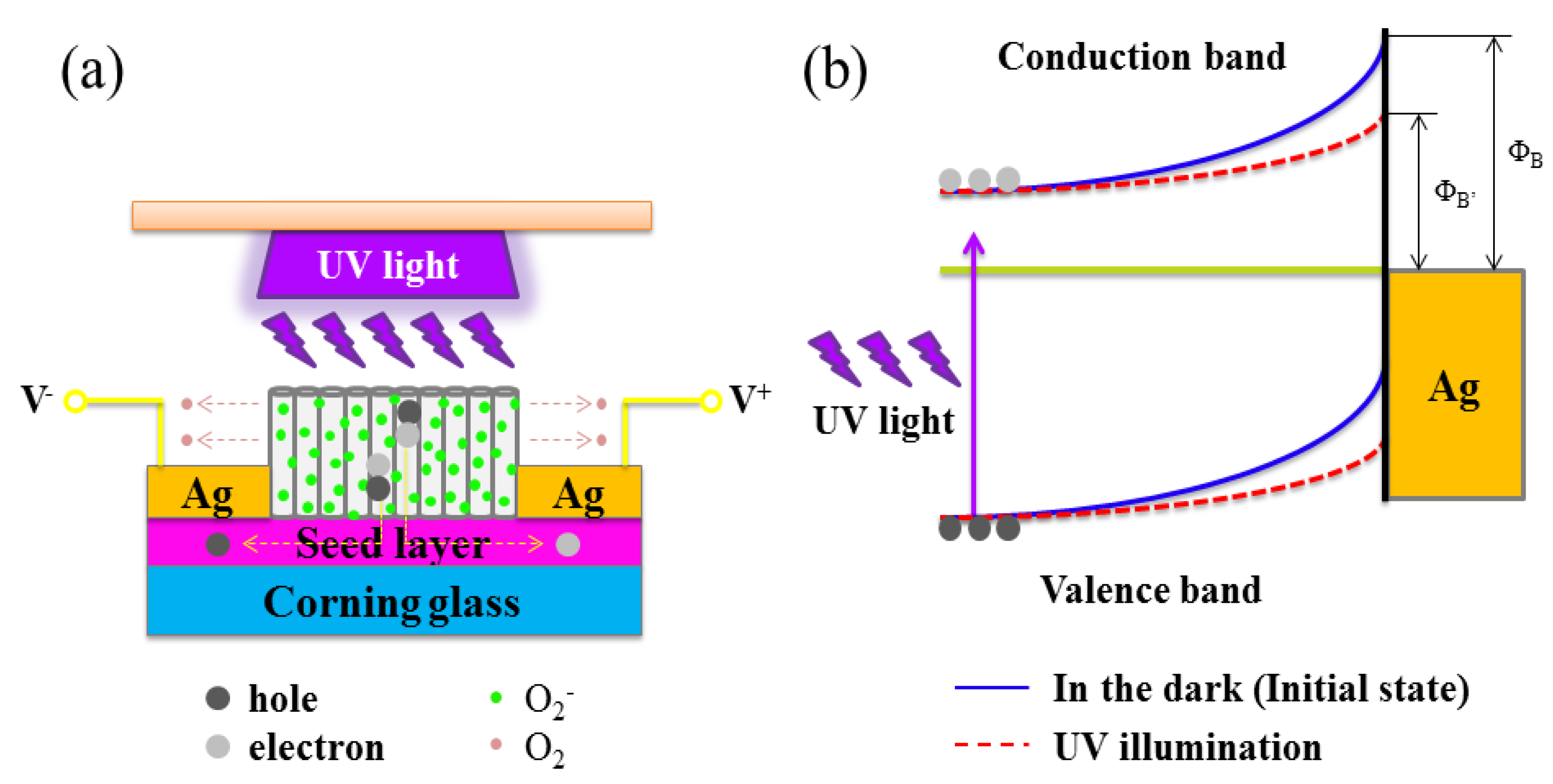
3. Results and Discussion
4. Conclusions
Author Contributions
Funding
Acknowledgments
Conflicts of Interest
References
- Amaro-Ortiz, A.; Yan, B.; D’Orazio, J.A. Ultraviolet Radiation, Aging and the Skin: Prevention of Damage by Topical cAMP Manipulation. Molecules 2014, 19, 6202–6219. [Google Scholar] [CrossRef] [PubMed]
- D’Orazio, J.; Jarrett, S.; Amaro-Ortiz, A.; Scott, T. UV Radiation and the Skin. Int. J. Mol. Sci. 2013, 14, 12222–12248. [Google Scholar] [CrossRef] [PubMed] [Green Version]
- Chu, T.T.; Jiang, H.L.; Ji, L.W.; Fang, T.H.; Shih, W.S.; Chang, T.L.; Meen, T.H.; Zhong, J.C. Characterization of UV photodetectors with MgxZn1-xO thin films. Microelectron. Eng. 2010, 87, 1777–1780. [Google Scholar] [CrossRef]
- Young, S.J.; Ji, L.W.; Chang, S.J.; Du, X.L. ZnO Metal-Semiconductor-Metal Ultraviolet Photodiodes with Au Contacts. J. Electrochem. Soc. 2017, 154, H26–H29. [Google Scholar] [CrossRef] [Green Version]
- Aldalbahi, A.; Li, E.; Rivera, M.; Velazquez, R.; Altalhi, T.; Peng, X.Y.; Feng, P.X. A new approach for fabrications of SiC based photodetectors. Sci. Rep. 2016, 6, 23457. [Google Scholar] [CrossRef]
- Liu, L.; Yang, C.; Patane, A.; Yu, Z.G.; Yan, F.G.; Wang, K.Y.; Lu, H.X.; Li, J.M.; Zhao, L.X. High-detectivity Ultraviolet Photodetectors based on Laterally Mesoporous GaN. Nanoscale 2017, 9, 8142–8148. [Google Scholar] [CrossRef] [Green Version]
- Nayef, U.M.; Hubeatir, K.A.; Abdulkareem, Z.J. Ultraviolet photodetector based on TiO2 nanoparticles/porous silicon hetrojunction. Optik 2016, 127, 2806–2810. [Google Scholar] [CrossRef]
- Chu, Y.L.; Ji, L.W.; Lu, H.Y.; Young, S.J.; Tang, I.T.; Chu, T.T.; Guo, J.S.; Tsai, Y.T. Fabrication and Characterization of UV Photodetectors with Cu-Doped ZnO Nanorod Arrays. J. Electrochem. Soc. 2020, 167, 027522. [Google Scholar] [CrossRef]
- Huang, C.H.; Chu, Y.L.; Ji, L.W.; Tang, I.T.; Chu, T.T.; Chiou, B.J. Fabrication and characterization of homostructured photodiodes with Li-doped ZnO nanorods. Microsyst. Technol. 2020, 1. [Google Scholar] [CrossRef]
- Espid, E.; Adeli, B.; Taghipour, F. Enhanced Gas Sensing Performance of Photo-Activated, Pt-Decorated, Single-Crystal ZnO Nanowires. J. Electrochem. Soc. 2019, 166, H3223–H3230. [Google Scholar] [CrossRef]
- Young, S.J.; Wang, T.H. ZnO Nanorods Adsorbed with Photochemical Ag Nanoparticles for IOT and Field Electron Emission Application. J. Electrochem. Soc. 2018, 165, B3043–B3045. [Google Scholar] [CrossRef]
- Chu, Y.L.; Ji, L.W.; Hsiao, Y.J.; Lu, H.Y.; Young, S.J.; Tang, I.T.; Chu, T.T.; Chen, X.J. Fabrication and Characterization of Ni-Doped ZnO Nanorod Arrays for UV Photodetector Application. J. Electrochem. Soc. 2020, 167, 067506. [Google Scholar] [CrossRef]
- Lam, K.T.; Chu, Y.L.; Ji, L.W.; Hsiao, Y.J.; Chu, T.T.; Huang, B.W. Characterization of nanogenerators based on S-doped zinc oxide nanorod arrays. Microsyst. Technol. 2020. [Google Scholar] [CrossRef]
- Young, S.J.; Tang, W.L. Wireless Zinc Oxide Based pH Sensor System. J. Electrochem. Soc. 2019, 166, B3047–B3050. [Google Scholar] [CrossRef]
- Kim, W.; Chu, K.S. ZnO nanowire field-effect transistor as a UV photodetector, optimization for maximum sensitivity. Phys. Status Solidi A 2009, 206, 179–182. [Google Scholar] [CrossRef]
- Shan, F.K.; Shin, B.C.; Jang, S.W.; Yu, Y.S. Substrate effects of ZnO thin films prepared by PLD technique. J. Eur. Ceram. Soc. 2004, 24, 1015–1018. [Google Scholar] [CrossRef]
- Kim, J.B.; Byun, D.; Ie, S.Y.; Park, D.H.; Choi, W.K.; Choi, J.W.; Angadi, B. Cu-doped ZnO-based p–n hetero-junction light emitting diode. Semicond. Sci. Technol. 2008, 23, 095004. [Google Scholar] [CrossRef]
- Chikoidze, E.; Modreanu, M.; Sallet, V.; Gorochov, O.; Galtier, P. Electrical properties of chlorine-doped ZnO thin films grown by MOCVD. Phys. Status Solidi A 2008, 205, 1575–1579. [Google Scholar] [CrossRef]
- Zhao, J.K.; Ge, S.S.; Pan, D.; Pan, Y.L.; Murugadoss, V.; Li, R.J.; Xie, W.; Lu, Y.; Wu, T.T.; Wujcik, E.K.; et al. Microwave Hydrothermal Synthesis of In2O3-ZnO Nanocomposites and Their Enhanced Photoelectrochemical Properties. J. Electrochem. Soc. 2019, 166, H3074–H3083. [Google Scholar] [CrossRef]
- Kim, D.C.; Jung, B.O.; Kwon, Y.H.; Cho, H.K. Highly Sensible ZnO Nanowire Ultraviolet Photodetectors Based on Mechanical Schottky Contact. J. Electrochem. Soc. 2011, 159, K10–K14. [Google Scholar] [CrossRef]
- Wang, R.C.; Hou, Y.R.; Liu, J.Y.; Chen, Y.W. Differentiating Ammonia from Other Reducing Gases via Response Reversal Phenomena by Varied ZnO/CuxO Nanorod Arrays. J. Electrochem. Soc. 2018, 165, B484–B490. [Google Scholar] [CrossRef]
- Young, S.J.; Yuan, K.W. Self-Powered ZnO Nanorod Ultraviolet Photodetector Integrated with Dye-Sensitised Solar Cell. J. Electrochem. Soc. 2019, 166, B1034–B1037. [Google Scholar] [CrossRef]
- Anitha, R.; Ramesh, R.; Loganathan, R.; Vavilapalli, D.S.; Baskar, K.; Singh, S. Large area ultraviolet photodetector on surface modified Si:GaN layers. Appl. Surf. Sci. 2018, 435, 1057–1064. [Google Scholar]
- Rambu, A.P.; Nica, V.; Dobromir, M. Influence of Fe-doping on the optical and electrical properties of ZnO films. Superlattice Microst. 2013, 59, 87–96. [Google Scholar] [CrossRef]
- Zhang, W.H.; Zhang, W.D.; Zhou, J.F. Solvent thermal synthesis and gas-sensing properties of Fe-doped ZnO. J. Mater. Sci. 2010, 45, 209–215. [Google Scholar] [CrossRef]
- Liu, C.W.; Chang, S.J.; Hsiao, C.H.; Liu, C.C.; Huang, R.J.; Lin, Y.S.; Su, M.C.; Wang, P.H.; Lo, K.Y. Diluted Magnetic Nanosemiconductor: Fe-Doped ZnO Vertically Aligned Nanorod Arrays Grown by Hydrothermal Synthesis. IEEE Trans. Nanotechnol. 2013, 12, 649–655. [Google Scholar] [CrossRef]
- Sahai, A.; Kumar, Y.; Agarwal, V.; Olive-Mendez, S.F.; Goswami, N. Doping concentration driven morphological evolution of Fe doped ZnO nanostructures. J. Appl. Phys. 2014, 116, 164315. [Google Scholar] [CrossRef]
- Yu, A.; Qian, J.S.; Pan, H.; Cui, Y.M.; Xu, M.G.; Tu, L.; Chai, Q.L.; Zhou, X.F. Micro-lotus constructed by Fe-doped ZnO hierarchically porous nanosheets: Preparation, characterization and gas sensing property. Sens. Actuat. B Chem. 2011, 158, 9–16. [Google Scholar] [CrossRef]
- Chand, P.; Gaur, A.; Kumar, A.; Gaur, U.K. Structural, morphological and optical study of Li doped ZnO thin films on Si (100) substrate deposited by pulsed laser deposition. Ceram. Int. 2014, 40, 11915–11923. [Google Scholar] [CrossRef]
- Chey, C.O.; Masood, A.; Riazanova, A.; Liu, X.; Rao, K.V.; Nur, O.; Willander, M. Synthesis of Fe-Doped ZnO Nanorods by Rapid Mixing Hydrothermal Method and Its Application for High Performance UV Photodetector. J. Nanomater. 2014, 2014, 524530. [Google Scholar] [CrossRef]
- Dom, R.; Baby, L.R.; Kim, H.G.; Borse, P.H. Fe controlled charge-dynamics in ZnO for solar hydrogen generation. Int. J. Hydrog. Energy 2017, 42, 5758–5767. [Google Scholar] [CrossRef]
- Wang, D.; Seo, H.W.; Tin, C.C.; Bozack, M.J.; Williams, J.R.; Park, M.; Sathitsuksanoh, N.; Cheng, A.J.; Tzeng, Y.H. Effects of postgrowth annealing treatment on the photoluminescence of zinc oxide nanorods. J. Appl. Phys. 2006, 99, 113509. [Google Scholar] [CrossRef]
- Yang, Z.X.; Zhong, W.; Au, C.T.; Du, X.; Song, H.A.; Qi, X.S.; Ye, X.J.; Xu, M.H.; Du, Y.W. Novel Photoluminescence Properties of Magnetic Fe/ZnO Composites: Self-Assembled ZnO Nanospikes on Fe Nanoparticles Fabricated by Hydrothermal Method. J. Phys. Chem. C 2009, 113, 21269–21273. [Google Scholar] [CrossRef]
- Saha, S.; Gupta, V. Al and Fe co-doped transparent conducting ZnO thin film for mediator-less biosensing application. AIP Adv. 2001, 1, 042112. [Google Scholar] [CrossRef]
- Hassan, M.M.; Khan, W.; Azam, A.; Naqvi, A.H. Effect of size reduction on structural and optical properties of ZnO matrix due to successive doping of Fe ions. J. Lumin. 2014, 145, 160–166. [Google Scholar] [CrossRef]
- Liu, Y.H.; Young, S.J.; Ji, L.W.; Chang, S.J. Noise Properties of Mg-Doped ZnO Nanorods Visible-Blind Photosensors. IEEE J. Sel. Topics Quantum Electron. 2015, 21, 3800405. [Google Scholar] [CrossRef]
- Bera, A.; Basak, D. Carrier relaxation through two-electron process during photoconduction in highly UV sensitive quasi-one-dimensional ZnO nanowires. Appl. Phys. Lett. 2008, 93, 053102. [Google Scholar] [CrossRef]
- Young, S.J.; Liu, Y.H. Ultraviolet Photodetectors With 2-D Indium-Doped ZnO Nanostructures. IEEE Trans. Electron Devices 2016, 63, 3160–3164. [Google Scholar] [CrossRef]
- Wu, C.Z.; Ji, L.W.; Peng, S.M.; Chen, Y.L.; Young, S.J. MgZnO Nanorod Homojunction Photodetectors for Solar-Blind Detection. Electrochem. Solid-State Lett. 2011, 14, J55–J57. [Google Scholar] [CrossRef]
- Heitz, R.; Hoffmann, A.; Broser, I. Fe3+ center in ZnO. Phys. Rev. B 1992, 45, 8997. [Google Scholar] [CrossRef]
- Ji, L.W.; Peng, S.M.; Su, Y.K.; Young, S.J.; Wu, C.Z.; Cheng, W.B. Ultraviolet photodetectors based on selectively grown ZnO nanorod arrays. Appl. Phys. Lett. 2009, 94, 203106. [Google Scholar] [CrossRef]
- Peng, S.M.; Su, Y.K.; Ji, L.W.; Wu, C.Z.; Cheng, W.B.; Chao, W.C. ZnO Nanobridge Array UV Photodetectors. J. Phys. Chem. C 2010, 114, 3204–3208. [Google Scholar] [CrossRef]
- Bai, S.L.; Guo, T.; Zhao, Y.B.; Sun, J.H.; Li, D.Q.; Chen, A.F.; Liu, C.C. Sensing performance and mechanism of Fe-doped ZnO microflowers. Sens. Actuat. B Chem. 2014, 195, 657–666. [Google Scholar] [CrossRef]
- Guo, W.W. Design of Gas Sensor Based on Fe-Doped ZnO Nanosheet-Spheres for Low Concentration of Formaldehyde Detection. J. Electrochem. Soc. 2016, 163, B517–B525. [Google Scholar] [CrossRef]
- Chen, T.P.; Young, S.J.; Chang, S.J.; Hsiao, C.H. Photoconductive Gain of Vertical ZnO Nanorods on Flexible Polyimide Substrate by Low-Temperature Process. IEEE Sens. J. 2011, 11, 3457–3461. [Google Scholar] [CrossRef]
- Chen, T.P.; Young, S.J.; Chang, S.J.; Hsiao, C.H.; Huang, C.S. Field-Emission and Photoelectrical Characteristics of ZnO Nanorods Photodetectors Prepared on Flexible Substrate. J. Electrochem. Soc. 2012, 159, J153–J157. [Google Scholar] [CrossRef]
- Hsiao, C.H.; Huang, C.S.; Young, S.J.; Chang, S.J.; Guo, J.J.; Liu, C.W.; Yang, T.Y. Field-Emission and Photoelectrical Characteristics of Ga–ZnO Nanorods Photodetector. IEEE Trans. Electron Dev. 2013, 60, 1905–1910. [Google Scholar] [CrossRef]
- Chang, S.J.; Liu, C.W.; Hsiao, C.H.; Lo, K.Y.; Young, S.J.; Kao, T.H.; Tsai, K.S.; Wu, S.L. Noise Properties of Fe-ZnO Nanorod Ultraviolet Photodetectors. IEEE Photon. Technol. Lett. 2013, 25, 2089. [Google Scholar] [CrossRef]
- Kumar, N.; Srivastava, A. Faster photoresponse, enhanced photosensitivity and photoluminescence in nanocrystalline ZnO films suitably doped by Cd. J. Alloys Compd. 2017, 706, 438–446. [Google Scholar] [CrossRef]
- Kumar, N.; Srivastava, A. Green photoluminescence and photoconductivity from screen-printed Mg doped ZnO films. J. Alloys Compd. 2018, 735, 312–318. [Google Scholar] [CrossRef]


| PD Samples | τr1 (s) | τr2 (s) | τd1 (s) | τd2 (s) | Idark (A) | Iphoto (A) | Sensitivity |
|---|---|---|---|---|---|---|---|
| Pure ZnO | 17 | 99 | 21 | 103 | 6.89 × 10⁻⁶ | 2.97 × 10⁻⁴ | 43.1 |
| FZO | 2 | 46 | 2 | 37 | 2.25 × 10⁻⁶ | 1.06 × 10⁻³ | 471.1 |
| MOS Structures | Bias (V) | Sensitivity (Iph/Id) | Rise Time (s) | Decay Time (s) | Responsivity (A/W) | Ref. |
|---|---|---|---|---|---|---|
| Ni-ZnO NRs | 3 | 393.04 | 70 | 43 | 2.10 | [12] |
| Ga-ZnO NRs | 1 | 11.7 | 29.75 | 89.67 | <0.05 | [47] |
| Pure ZnO NRs | 1 | <10 | 42.9 | 132.9 | × | [48] |
| Fe-ZnO NRs | 1 | ~49 | 21.2 | 24.7 | 0.06 | [48] |
| 2 at% Cd-ZnO film | 5 | 93.78 | 37.03 | 221.93 | × | [49] |
| 15 at% Mg-ZnO film | 5 | 71.68 | 381 | 122.5 | × | [50] |
| FZO NRs | 3 | 471.1 | 46 | 37 | 0.758 | Present |
© 2020 by the authors. Licensee MDPI, Basel, Switzerland. This article is an open access article distributed under the terms and conditions of the Creative Commons Attribution (CC BY) license (http://creativecommons.org/licenses/by/4.0/).
Share and Cite
Chu, Y.-L.; Young, S.-J.; Ji, L.-W.; Tang, I.-T.; Chu, T.-T. Fabrication of Ultraviolet Photodetectors Based on Fe-Doped ZnO Nanorod Structures. Sensors 2020, 20, 3861. https://doi.org/10.3390/s20143861
Chu Y-L, Young S-J, Ji L-W, Tang I-T, Chu T-T. Fabrication of Ultraviolet Photodetectors Based on Fe-Doped ZnO Nanorod Structures. Sensors. 2020; 20(14):3861. https://doi.org/10.3390/s20143861
Chicago/Turabian StyleChu, Yen-Lin, Sheng-Joue Young, Liang-Wen Ji, I-Tseng Tang, and Tung-Te Chu. 2020. "Fabrication of Ultraviolet Photodetectors Based on Fe-Doped ZnO Nanorod Structures" Sensors 20, no. 14: 3861. https://doi.org/10.3390/s20143861