1. Introduction
Micro-electromechanical system (MEMS) resonators have been intensively investigated in recent years for an increasing number of applications, ranging from timing [
1], filtering [
2], and actuating to sensing [
3]. One advantage of the emerging adoption of MEMS resonators is their potential level of integration with current integrated circuit (IC) technology [
4] with respect to other devices, such as surface acoustic wave (SAW) [
5,
6] or quartz crystal [
7] resonators.
Different actuation and detection mechanisms have been adopted for MEMS resonators, such as electrostatic, magnetic, piezoresistive or piezoelectric [
8,
9]. In particular, piezoelectric materials, such as lead-zirconate-titanate (PZT) films, have been successfully deposited on silicon resonators, either as post-processed thick films [
10,
11,
12], or thin films [
13]. In addition, the deposition of other piezoelectric materials, such as zinc oxide (ZnO) or aluminum nitride (AlN) [
14], has been demonstrated. In particular, AlN thin-film piezoelectric-on-silicon (TPoS) resonators have attracted great interest because of their better compatibility with IC fabrication processes compared to both PZT and ZnO films [
15].
One additional advantage of piezoelectric resonators, especially when operated as sensors, is their suitability for contactless interrogation, i.e., excitation and detection of mechanical resonances without required wired connections [
16]. Contactless operation is particularly attractive when cabled connections are unpractical, such as operation in closed environments, sealed packages or in-liquid operation in enclosed volumes. Contactless interrogation exploits the magnetic coupling between a readout coil, which is coupled to the reading circuitry forming the interrogation unit, and a sensor coil, which is connected to the piezoelectric resonator forming the sensor unit. Effective contactless interrogation in real applications demands for the readout of the resonant frequency of the resonator to be independent from the stand-off distance between the interrogation and sensor units. For this purpose, techniques both in the frequency [
17] and time [
18] domains have been investigated.
Frequency domain techniques typically rely on simultaneous excitation and detection phases with a reflected impedance measured at the readout coil [
19,
20]. Time domain techniques, also referred to as time-gated, excite the sensor for a finite time duration, and then detect the decaying resonant response, from which the resonant frequency and possibly the quality factor are extracted. Both techniques, besides being applicable also to capacitive sensors [
17], have been demonstrated to be to first order independent from the interrogation distance. Additionally, residual dependence on the distance, mainly due to parasitic capacitance in parallel to the readout coil introduced by electrical connections and the front-end electronic circuit, can be mitigated electronically by suitable compensation circuits [
21].
In this work the time-gated contactless interrogation technique is innovatively applied to a TPoS contour-mode MEMS resonator based on AlN [
22,
23]. The resonator is operated in one-port configuration and the proposed technique is verified and experimentally validated through a purposely-designed electronic circuit that is tailored to the electrical parameters of the microresonator. The TPoS resonator is applied as a sensor to the measurement of ambient temperature and the detection of acoustic loading due to microdroplets of deionized (DI) water deposited on the resonator top surface, with real-time tracking of the subsequent evaporation. The proposed system can advantageously operate as a stand-alone device which can be electromagnetically linked for interrogation, without requiring on-board active electronics. The fabrication of the AlN TPoS resonator, the results of finite element simulations, the operating principle of the contactless interrogation technique and electronic circuit, the results of the experimental characterization and the conclusions are reported in
Section 2,
Section 3,
Section 4,
Section 5 and
Section 6, respectively.
Appendix A summarizes the main symbols adopted in the paper.
2. Technology and Fabrication Processes
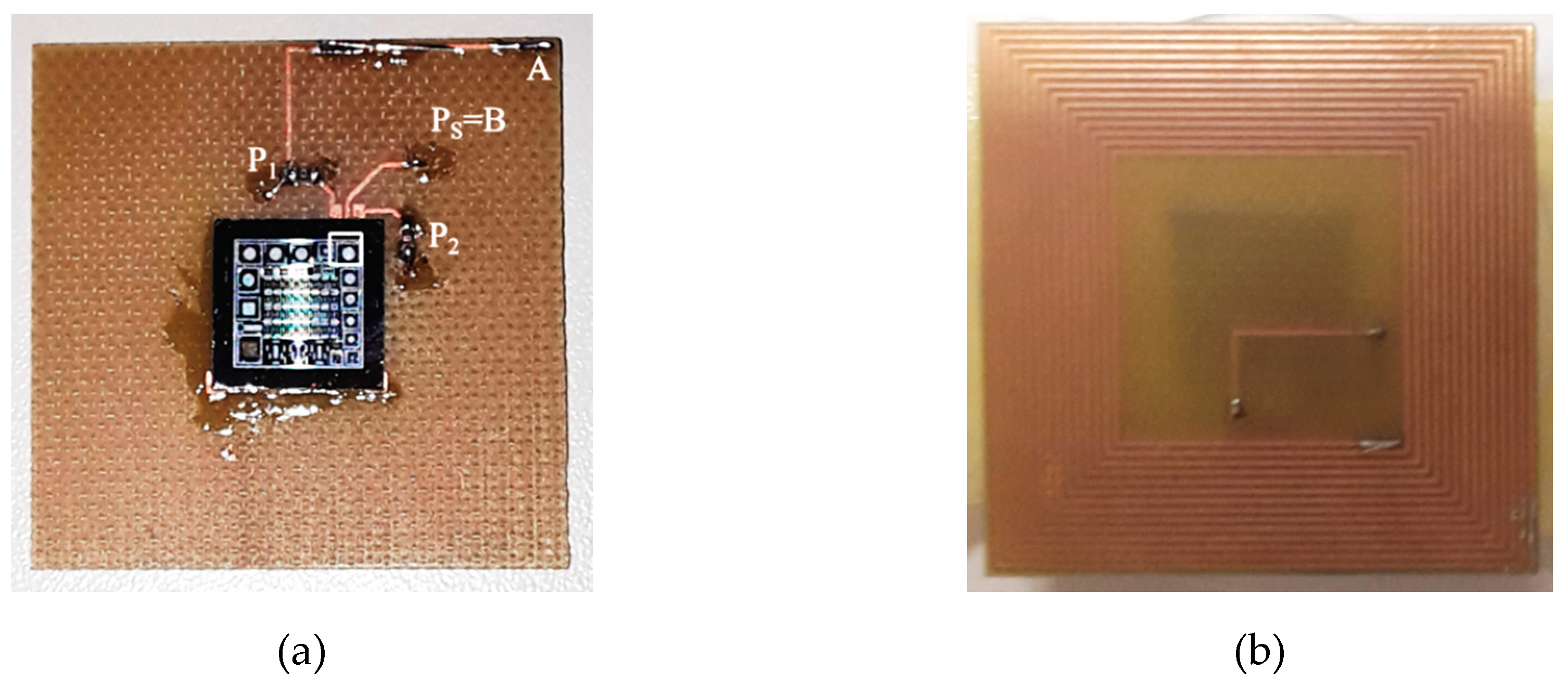
Figure 1a shows the optical micrograph of the adopted MEMS resonator seen from the top. The MEMS resonator is an AlN TPoS disk with a radius of 400 µm, fabricated using the PiezoMUMPs (Piezo Multi-User MEMS Processes) foundry process offered by MEMSCAP [
24]. The process begins with a silicon-on-insulator (SOI) wafer and a silicon device layer (Si) that is 10-µm thick. The device layer is a surface-doped n-type layer in order to create an ohmic layer in a subsequent metallization stage to define the contact pads and electrodes. A 200-nm-thick thermal oxide is grown and patterned by reactive ion etching as an insulation layer on the silicon device layer, as depicted in
Figure 1b. This is then followed by deposition of AlN as the piezoelectric material by reactive sputtering with a thickness of 500 nm. The AlN layer is patterned by wet etching. The use of AlN has the advantage of having the potential for chip level integration and CMOS compatibility compared to other piezoelectric materials like PZT and ZnO. The 10-µm-thick silicon layer increases energy storage to the resonator compared to a structure that is comprised of only AlN, which generally yields higher quality factors. Next, a metal stack of 20-nm-thick Cr and 1-µm-thick Al is patterned and deposited by a lift-off process to define the contact pads and top electrodes of the resonator, as shown in
Figure 1c. Next, the silicon device layer is lithographically patterned and etched by deep reactive ion etching (DRIE) to define the features of the resonator as depicted in
Figure 1d. This includes the T-shape tethers on 4 sides of the disk resonator for supporting the structures, as indicated in
Figure 1a. The resonator has to be supported from the sides in this case as it is not possible to clamp the structure from the center due to the release method. To release the structure from the substrate, the top side of the wafer is covered with a protective polymer coat first. The back of the SOI wafer is lithographically patterned to define the opening of a cavity, through which the handling layer of the wafer is trench etched by DRIE followed by wet oxide removal of the buried oxide layer. The front side protective coat is then removed to release the device, as shown in
Figure 1e, followed by dicing. In this case, the back cavity is circular, which can be viewed in
Figure 1a as the dark ring around the TPoS disk. The two Al top electrodes P
1 and P
2, and the bottom ground electrode P
S allow the operation of the device as either a two-port resonator or, by shorting P
1 and P
2, as a one-port resonator between the connections A and B, as shown in
Figure 1e. By relating the top view of the device in
Figure 1a, with a side view schematic in
Figure 1e, it can be seen that the contact pads of P
1 and P
2 are isolated from the silicon device layer by 200-nm thermal oxide, while the wide frame tracks around the resonator contact the silicon device layer as grounding pads (P
S).
3. FEM Simulations
The considered device, with the configuration of the electrodes shown in
Figure 1b, vibrates in the so-called radial contour mode. The device was investigated by finite element (FE) analysis simulations using COMSOL Multiphysics. An eigenfrequency analysis to compute the mode shape (eigenfunction) and corresponding modal frequency (eigenfrequency) was performed first.
Figure 2a shows the total displacement profile of the fundamental radial contour mode, which can be described by the disk contracted and expanding radially with a nodal point at the center.
Figure 2b shows the corresponding distribution of the sum of lateral strains, where the maximum strain is concentrated at the center of the disk for the radial contour mode. The resonant frequency scales inversely with the diameter or radius of the disk. The elasticity properties and density of the structure, which determine the resonant frequency, are dominated by the silicon device layer, which is much thicker than the other constituent layers. In the FE model, to compute the resonant frequency, the elastic matrix of single-crystal silicon for the (100) plane, based on the material properties reported in reference [
25], has been adopted instead of assuming isotropic elasticity. In the case of the device presented in this paper, which has a disk radius of 400 µm, the resonant frequency of the radial contour mode obtained by FE is 6.32 MHz.
Subsequently, a frequency domain analysis was performed to compute the electrical admittance
Y = G + j
B of the resonator, where
G and
B are the conductance and susceptance, respectively. For this purpose, the resonator was driven by a harmonic fixed-frequency voltage across A and B to determine the corresponding value of electrical admittance. By sweeping the driving frequency in the range from 6.310 to 6.330 MHz, the spectra of
G and
B were derived as shown in
Figure 3a. The electromechanical behavior of the TPoS resonator can be modeled around its resonant frequency through the equivalent Butterworth–van Dyke (BVD) circuit of
Figure 3b. The BVD circuit is composed of an electrical branch formed by the capacitance
C0 plus a motional branch in parallel. The motional branch comprises the series inductance
Lm, capacitance
Cm and resistance
Rm, which represent the equivalent mass, compliance and energy losses of the resonator, respectively [
9]. The values of
Y from the simulation have been fitted with the corresponding expressions of
G and
B given by Equations (1) and (2):
where
f is the frequency in hertz. From the fitting, the values of the parameters of the equivalent BVD circuit have been estimated. The resulting fitted curves and the estimated parameters are shown in
Figure 3a. From these values, the resonant frequency and the quality factor of the resonator can be calculated as Equations (3) and (4):
Accordingly, the simulated resonant frequency and the quality factor result fS,sim = 6.318 MHz and Qsim = 1222, respectively.
4. Operating Principle of the Interrogation Technique and Electronic Circuit
Figure 4 shows the block diagram of the developed contactless interrogation system, which is composed of an interrogation unit (IU) and a sensor unit (SU). The IU is in turn composed of two programmable direct digital synthesizers (DDSs) named DDS1 and DDS2, fed by the common clock CLK, which generate the relevant signals for system operation. DDS1 generates the sinusoidal waveform
ve(
t) at frequency
fe, gated by the square waveform
vg(
t), with period
Tg =
Te +
Td generated by DDS2. During the time interval
Te, the interrogation system is in the excitation phase. Consequently, the switch SW is closed and the fully differential amplifier U
1 drives the readout coil, modeled by the inductance
L1 and series resistance
R1. During the time interval
Td, the interrogation system is in the detection phase. The switch SW is open and the readout signal
vd(
t) across the readout coil is sensed by the high-impedance amplifier U
2 and amplified with gain
GA = 8. The output voltage
vo(
t) is fed to a frequency counter to obtain the readout frequency
fout.
The readout coil is electromagnetically air-coupled to the sensor coil modeled by the inductance L2 and series resistance R2. The magnetic coupling between L1 and L2 is represented by the mutual inductance M = k(L1L2)1/2, where k is the coupling factor. The sensor coil is connected to the resonator represented by its BVD circuit. The sensor coil and the resonator form the SU.
During the excitation phase, through the electromagnetic coupling between
L1 and
L2, the sensor is excited at a frequency
fe proximal to its series resonant frequency given by Equation (3), i.e.,
fe ≈
fS. During the detection phase, the excitation signal is disconnected, and the resonator undergoes decaying oscillations at the damped frequency
fdm, forcing a current in
L2. Consequently, an induced readout voltage
vd(
t) can be sensed across
L1, i.e., at the input of U
2. It has been demonstrated that the signal
vd(
t) is the sum of two damped sinusoidal signals at frequency
fdm and
fde with exponential decay times
τm and
τe, respectively [
18]. The damped sinusoid at
fdm is due to the mechanical response of the resonator, while the damped sinusoid at
fde is due to
L2 resonating with
C0. Considering for the resonator the typical values of the BVD model of
Figure 3b, for suitable values of
L2 and
R2, it occurs that
τm >>
τe, i.e., the damped sinusoid at
fde decays rapidly to zero with respect to the damped sinusoid at
fdm. Hence, the contribution of the damped sinusoid at
fde to
vd(
t) can be neglected. In addition, assuming infinite input impedance of U
2, |
R2 + j2π
fSL2| << 1/(2π
fSC0) and
Rm << 1/(2π
fSC0), i.e., at
fS, the impedance of
C0 can be neglected with respect to the corresponding impedance of
R2-
L2, and to that of the motional branch
Rm-
Lm-
Cm of the BVD circuit, the following simplified expression for
vo(
t) can be derived [
18]:
where the amplitude and phase coefficients
Am and
θm are functions of both the initial conditions taken at the end of the excitation period and the electrical and mechanical parameters of the system composed of
R1,
L1,
R2,
L2 and the resonator. In Equation (5), the damped frequency is
fdm = [
fS2 − 1/(2π
τm)
2]
1/2, with
fS given by Equation (3), while
τm is related to the mechanical quality factor
Q of the resonator in Equation (4) by
Q = π
fSτm [
16]. It has been demonstrated [
18] that if
Lm >>
L2 and for
Q in the order of 1000, it results
fdm ≈
fS, with (
fS −
fdm)/
fS in the order of 10
−7. The additional term
GA in Equation (5) is a voltage impulse which accounts for the initial current in
L1.
It should be noticed that the exact knowledge of the resonant frequency of the resonator is not strictly required to set the excitation frequency fe because the measurement technique exploits the free response of the resonator which is independent of the type of excitation. However, if fe is close to fS, the signal-to-noise ratio (SNR) during the detection phase is enhanced, and hence, in principle, a higher interrogation distance d can be attained. Equation (5) also shows that vo(t) is proportional to fS and the mutual inductance M advantageously only acts as a scaling factor on the amplitude of the signal without affecting the value of fdm. This is a key feature of the proposed technique that makes it possible to derive fdm independently from the distance d. The frequency fdm can be measured through a frequency counter gated with the signal vg(t) to synchronize with the transient and give the readout frequency fout = fdm.
5. Results and Discussion
Preliminarily, the resonator was electrically characterized by measuring the real and imaginary parts of the admittance
Y =
G + j
B between A and B through contact probes by means of a HP4194A impedance analyzer (Palo Alto, CA, USA). The measurements were taken with the resonator in air at room temperature and atmosphere. The measured spectra of
G and
B around the frequency of the first vibration mode are reported in
Figure 5, where, consistently with the BVD model, the resonant frequency has been taken in correspondence of the maximum of
G, i.e.,
fS = 6.322 MHz. The parameters of the BVD equivalent circuit were extracted from the fitting of Y to the measured data, resulting in
Rm = 56.2 Ω,
Cm = 365 fF,
Lm = 1.79 mH,
C0 = 78.2 pF. From these values, a quality factor
Q = 1226 can be estimated. Compared to the FE simulation results, it can be observed that the experimental values of the parameters of the BVD circuit are in agreement within a few percent. Hence, it also results that
fS ≈
fS,sim and
Q ≈
Qsim.
Figure 6 shows the fabricated SU. A planar spiral coil has been milled from a copper-clad flame-retardant (FR4) substrate with dimensions of 35 mm × 35 mm. The coil has been electrically characterized at
fS, where it has an equivalent resistance
R2 = 7.23 Ω and inductance
L2 = 8.19 µH. The silicon chip with the TPoS resonator has been glued at the center of the spiral coil and bonded through gold wires to the connection pads.
A prototype of the IU, corresponding to the schematic diagram of
Figure 4, was fabricated. In particular, the IU adopts two AD9834 (Analog Devices, Norwood, MA, USA) for the DDSs, fed by a 40 MHz clock. The amplifiers U1 and U2 are an AD8139 (Analog Devices, Norwood, MA, USA) and an OPA656 (Texas Instruments, Dallas, TX, USA), respectively, while the switch SW is a MAX303 (Maxim Integrated, San Jose, CA, USA). The readout coil is a spiral coil on FR4 substrate with
R1 = 5.12 Ω and
L1 = 8.5 µH measured at
fS. The readout frequency
fout was measured by means of a PM6681 (Fluke, Everett, WA, USA) frequency counter.
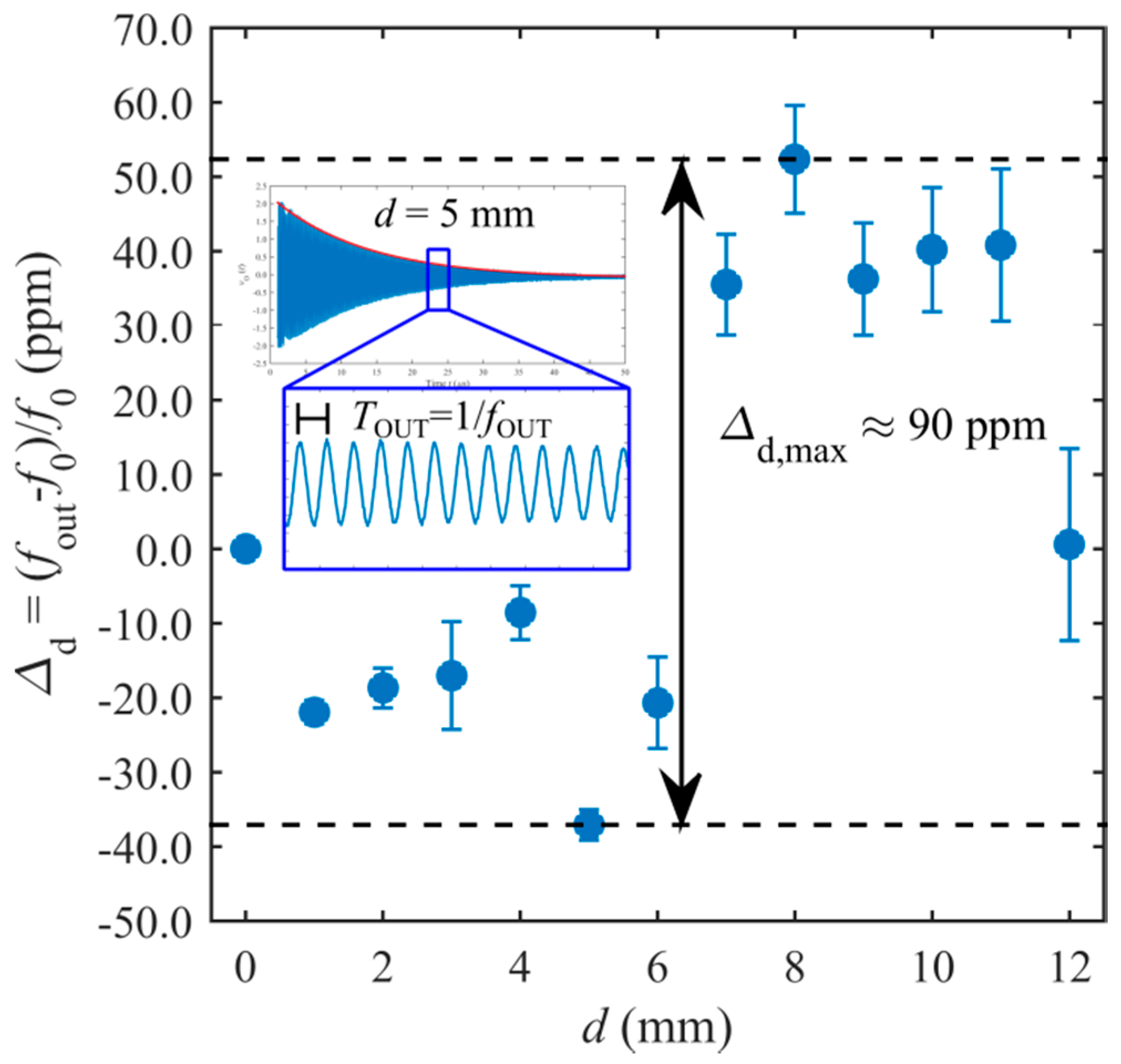
Initially, the system was tested to verify the independence of
fout from the interrogation distance
d. For this purpose, measurements were taken at several prescribed values of
d in the range between 0 mm and 12 mm.
Figure 7 reports the resulting
Δd = (
fout –
f0)/
f0, i.e., the measured relative deviation of
fout with respect to
f0 = 6.355 MHz, where
f0 corresponds to
fout at
d = 0 mm.
For each value of
d, ten repeated measurements have been acquired and the corresponding standard deviation
σ(
d) was calculated. The error bars in
Figure 7 represent the relative standard deviation, i.e.,
σ(
d)/
fout. As it can be observed, in the explored range of distances, the maximum variation of
Δd is about
Δd,max = 90 ppm, validating the theoretical predictions of the model in
Section 2, according to which
fout does not depend on
M, and hence, on
d. The residual difference between
f0 and
fS can be ascribed to secondary effects not accounted for in the proposed model of the interrogation principle. The inset of
Figure 7 shows the typical waveform of
vo(
t) during the detection phase, corresponding to
d = 5 mm. As expected,
vo(
t) is a damped sinusoid at frequency
fout = fdm.
To validate the interrogation principle and the capability of the TPoS resonator system to operate as a contactless sensor, two tests have been proposed and performed.
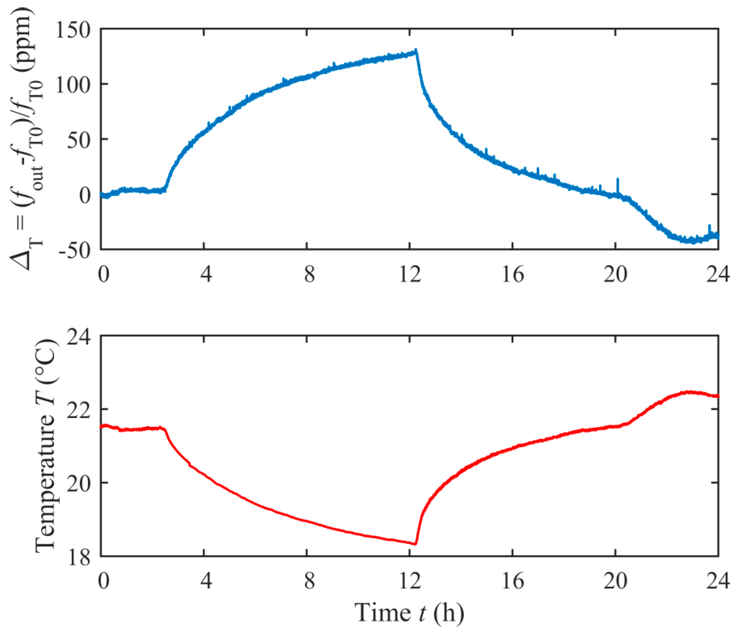
Firstly, the system was tested for temperature sensing, by acquiring
fout and the ambient temperature
T by means of a Pt1000 sensor close to the resonator.
Figure 8 shows
ΔT = (
fout –
fT0)/
fT0, i.e., the relative deviation of
fout with respect to
fT0, where
fT0 is
fout at
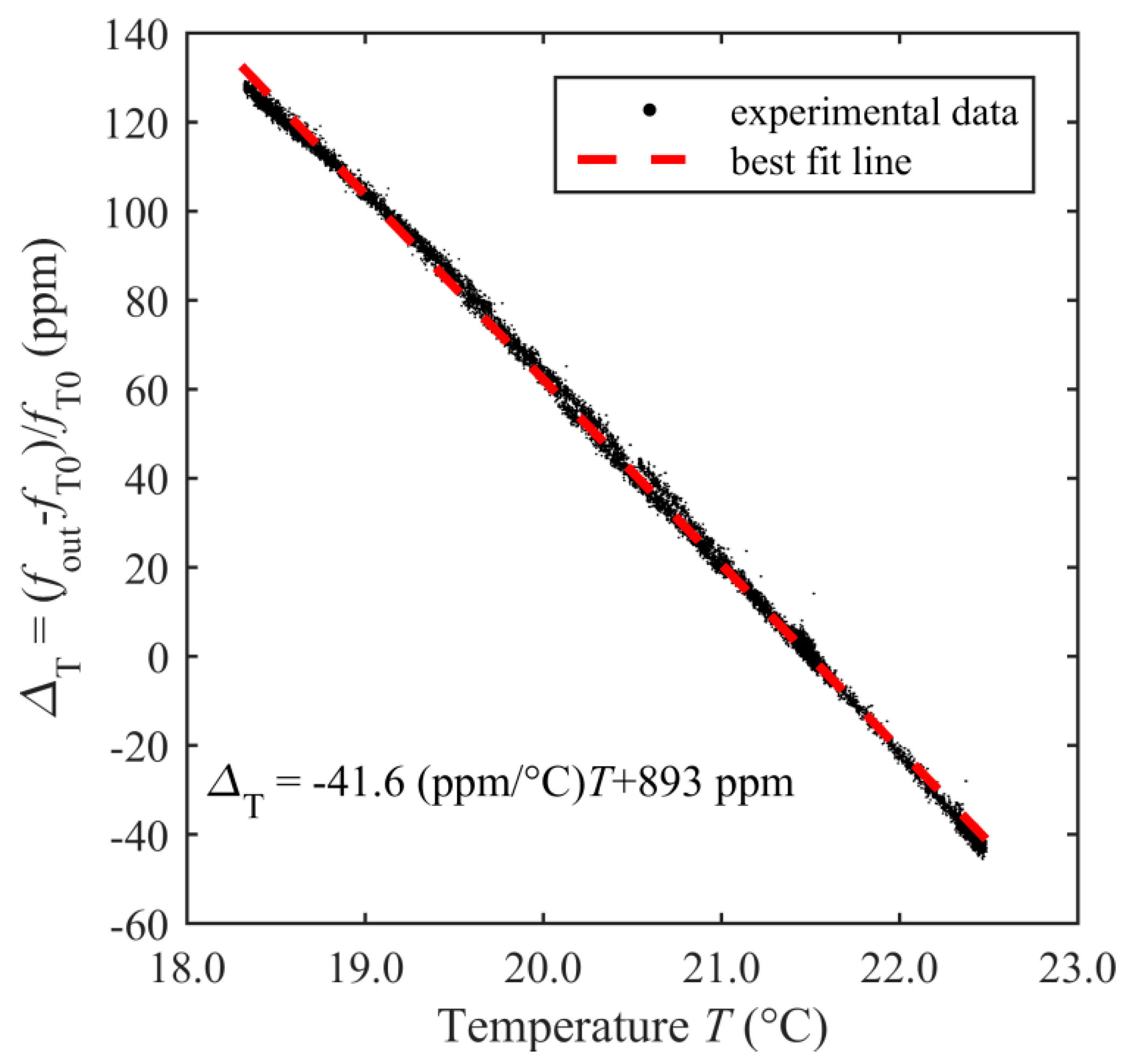
t = 0, over a period of 24 h, while the resonator undergoes ambient temperature changes. It can be observed that
ΔT follows the temperature
T, with an opposite correlation evidenced by
Figure 9, which plots
ΔT as a function of
T, similarly to the results in reference [
26]. The best fit line of the experimental data allows estimating, for the considered temperature range, a temperature coefficient of frequency (TCF) of −41.6 ppm/°C.
Subsequently, the system was applied to the measurement of frequency changes due to the deposition of different volumes of DI water microdroplets on the top surface of the TPoS resonator [
27].
Figure 10 shows the experimental setup, which adopts a MJ-AB-80 piezoelectric microdispenser (MicroFab Technologies, Inc., Plano, TX, USA) with 80-µm-diameter orifice to deposit 150 pl microdroplets of water on the sensor surface [
28]. The microdispenser was driven by a trapezoidal pulse train waveform by means of a programmable function generator and a custom designed power amplifier. Each driving pulse has an amplitude of 60 V and a duration of 25 μs, with rise and fall times of 3 μs, and this causes the ejection of a single droplet. The adopted pulse-train waveform was composed of
N pulses at the driving frequency of 250 Hz, with
N that can be set. The SU has been placed under a microscope to align the microdispenser to the resonator surface and take pictures of the microdroplets during the tests. The IU, and hence, the readout coil were kept at
d = 5 mm beneath the sensor coil for all the deposition tests.
The upper plot of
Figure 11 shows the measured values of
Δm = (
fout –
fm0)/
fm0 as a function of time for
N = 100, i.e., the relative deviation of
fout with respect to
fm0, where
fm0 is
fout at
t = 0, i.e., with no added microdroplets. It can be seen that the response of the resonator, considering also the transient behavior, has a complex pattern. The analysis of such a pattern requires sophisticated modeling [
27] which is not considered in the present work that is dedicated to the validation of the time-gated technique innovatively coupled to TPoS resonators. Hence, in the following, only a qualitative discussion of the observed phenomena will be offered. For this purpose, in
Figure 11a–f, pictures are shown, taken in correspondence with selected events along the deposition and evaporation process of the droplets.
In particular, the pictures have been respectively taken as listed in the following: (a) at the beginning, when the resonator is dry, hence Δm = 0; (b) after the deposition of the droplets, hence Δm decreases; (c) after a transient, hence Δm settles to a steady state value depending on the amount of the deposited water which, in the meantime, evaporates; (d) when the drying of the surface begins and the water creates a thin film, hence Δm rises; (e) when the drying is almost complete, a fast change in Δm occurs, possibly to be ascribed to the visible change in the spatial distribution of the water film; (f) when the drying is complete, Δm returns to zero.
Similar responses have been measured for different volumes of deposited water, as shown in
Figure 12, which compares the cases
N = 20,
N = 50 and
N = 100, respectively. As expected, it can be observed that the initial decrease in
Δm is related to the volume of deposited water, and hence, to
N. Similarly, the period of time when
Δm has a steady value depends on
N, being related to the evaporation time.
It is remarkable that the proposed interrogation technique and system coupled to a TPoS resonator allows the detection of such complex behaviors as was possible with different resonators, namely quartz crystal resonators (QCRs) [
29] or resonant piezo-layers (RPLs) [
16]. Such an ability is partly due to the inherent speed of data acquisition allowed by the developed technique and electronic system compared to the other techniques, such as for example those based on impedance measurements, which require sampling and computation. In this respect, comparable results have also been obtained by adopting QCRs coupled to oscillator circuits [
30,
31,
32].
In the use of disks resonators as mass-sensitive sensors, it has to be considered that for them, as compared to QCRs and RPLs, due to the involved vibration mode, the mass sensitivity is inherently dependent on both the location and distribution of the added mass on the surface of the resonator. For a distributed mass, the change in frequency depends on the integral of the vibration velocity distribution over the area where the mass is spread [
33].

 ,
, 


