Article

Study of Metal–Semiconductor–Metal CH3NH3PbBr3 Perovskite Photodetectors Prepared by Inverse Temperature Crystallization Method

1
Department of Electro-optical Engineering, National Taipei University of Technology, 1, 3 Sec., Chung-Hsiao E. Rd., Taipei 10608, Taiwan
2
Department of Electrical Engineering, China University of Science and Technology, Taipei 11581, Taiwan
3
Department of Electronics, Chang Gung University, Wen-Hwa 1st Road, Kwei-Shan, Tao-Yuan 33302, Taiwan
*
Authors to whom correspondence should be addressed.
Sensors 2020, 20(1), 297; https://doi.org/10.3390/s20010297
Submission received: 11 December 2019 / Revised: 27 December 2019 / Accepted: 3 January 2020 / Published: 5 January 2020
(This article belongs to the Section Sensor Materials)

Abstract

:
Numerous studies have addressed the use of perovskite materials for fabricating a wide range of optoelectronic devices. This study employs the deposition of an electron transport layer of C60 and an Ag electrode on CH3NH3PbBr3 perovskite crystals to complete a photodetector structure, which exhibits a metal–semiconductor–metal (MSM) type structure. First, CH3NH3PbBr3 perovskite crystals were grown by inverse temperature crystallization (ITC) in a pre-heated circulator oven. This oven was able to supply uniform heat for facilitating the growth of high-quality and large-area crystals. Second, the different growth temperatures for CH3NH3PbBr3 perovskite crystals were investigated. The electrical, optical, and morphological characteristics of the perovskite crystals were analyzed by X-ray diffraction (XRD), scanning electron microscopy (SEM), ultraviolet-visible spectroscopy, and photoluminescence (PL). Finally, the CH3NH3PbBr3 perovskite crystals were observed to form a contact with the Ag/C60 as the photodetector, which revealed a responsivity of 24.5 A/W.

1. Introduction

Perovskite is a material that comprises an ABX3 structure. In this molecular formula, A, B, and X represent an alkali metal ion or a methylamine radical (CH3NH3), a metal cation (Pb2, Sn2), and a halogen cation (Cl-, Br-, I-), respectively. Compared with organic semiconductor materials, perovskite materials based on organic metal halides exhibit unique optical and electrical properties. It is well-established that the exciton binding energy of perovskite materials is extremely small; therefore, the majority of the excitons, which are generated after being excited by light, can be separated to form free electrons and holes at room temperature. Further, the carrier current possesses a fast diffusion speed and a long diffusion distance. The diffusion lengths of electrons and holes vary with the crystal structure. Compared with MAPbI3, MAPbBr3 has a shorter lattice constant, higher cohesion energy, lower phase transition temperature, and superior anisotropy [1]. The energy gap is approximately 2.2 eV, and the emission wavelength is green [2]. It has a significantly high optical gain and can be used as a gain dielectric layer in laser [3]. Perovskite materials have been successfully developed in light-emitting diodes [4,5,6,7] and solar cells [8,9,10,11,12]. Perovskite materials can be utilized for a wide range of applications in the field of optoelectronics. Thus far, various types of light sensors have been studied and consequently applied; these include various photodetectors and Schottky barrier diodes [13,14,15,16,17,18,19,20,21,22,23,24,25]. Metal–semiconductor–metal (MSM) structured light sensors or photodetectors have the advantages of a straightforward manufacturing process, high sensitivity, and high response speed as compared with sensors possessing other structures.
Therefore, this study employs CH3NH3PbBr3 perovskite crystals prepared by inverse temperature crystallization method. Conventional crystallization methods, such as the typical cooling or antisolvent vapor-assisted crystallization techniques, are time-consuming and have a long process period. In contrast, the inverse temperature crystallization (ITC) is a fast solution-based crystal growth method, and the optical, electrical, and crystal properties were comparable to the results of them [26,27,28]. C60/Ag electrodes were formed to produce a MSM structure for its required research path. The optoelectronic properties of the MSM-type CH3NH3PbBr3 perovskite photodetectors were then examined.

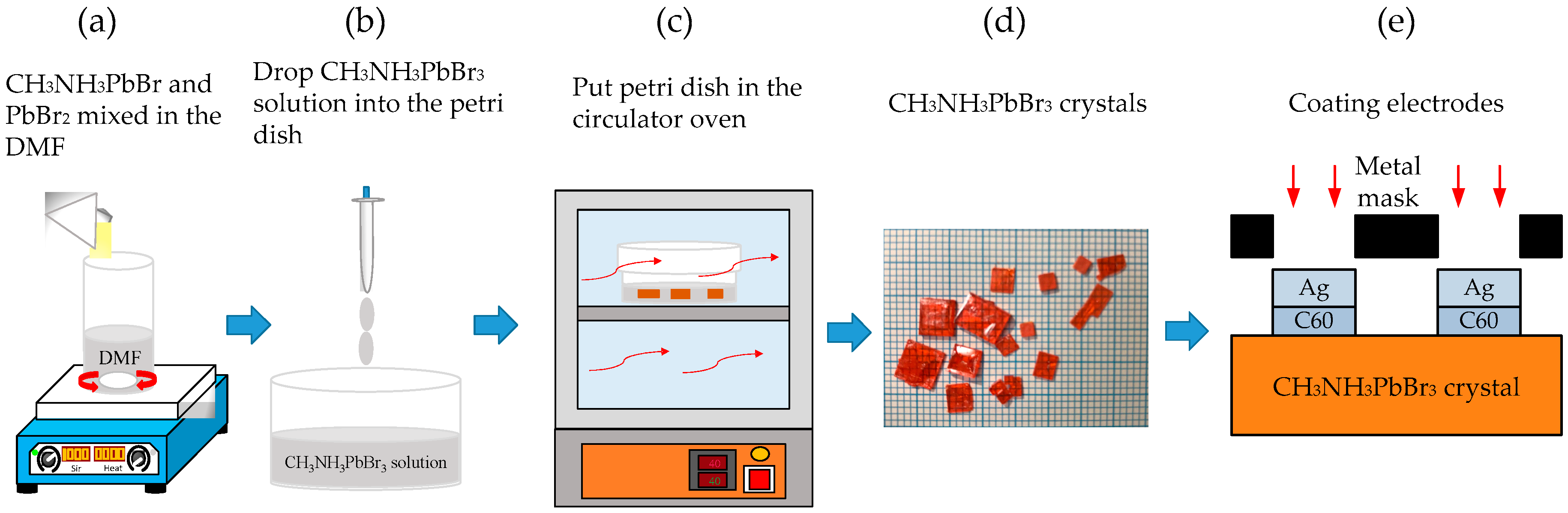
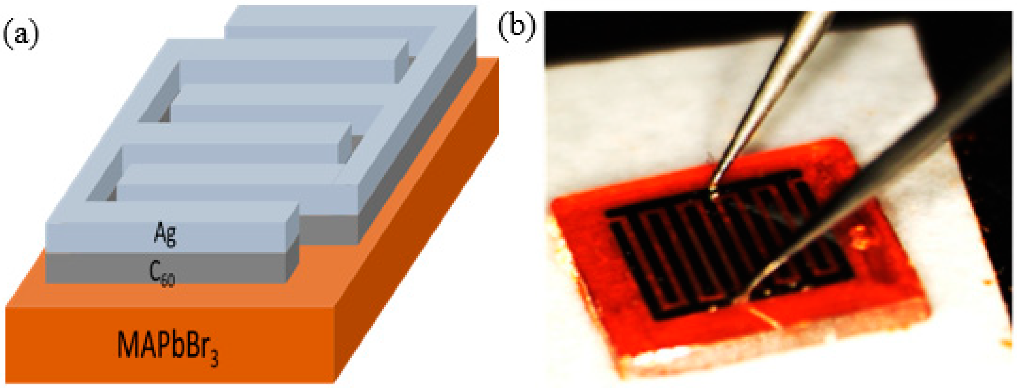
2. Materials and Methods

First of all, the CH3NH3PbBr3 perovskite precursor solution was prepared with the incorporation of 0.0367 g PbBr2 (99.998%), 0.0112 g CH3NH3Br2 (MAB, 99.9%), and 1 mL of dimethylformamide (DMF, 98%) solvent. Subsequently, the precursor solution was stirred until it turned clear. The Petri dishes were sonicated with acetone, alcohol, and isopropyl alcohol for 10 min. The precursor solution was then poured into the Petri dish and placed in the hot circulator oven at different temperatures, namely: 40 °C, 50 °C, 60 °C, 70 °C, and 80 °C. CH3NH3PbBr3 crystals were found to grow at a slow rate and gradually became larger during the crystal growth. Finally, the electron transport layer of 20 nm-thick C60 and the 100 nm-thick Ag electrodes were deposited on CH3NH3PbBr3 crystals via thermal evaporation and metal mask to complete the MSM structures with an interdigital finger electrode. Figure 1 presents the schematic diagram of the MSM photodetector process procedure.

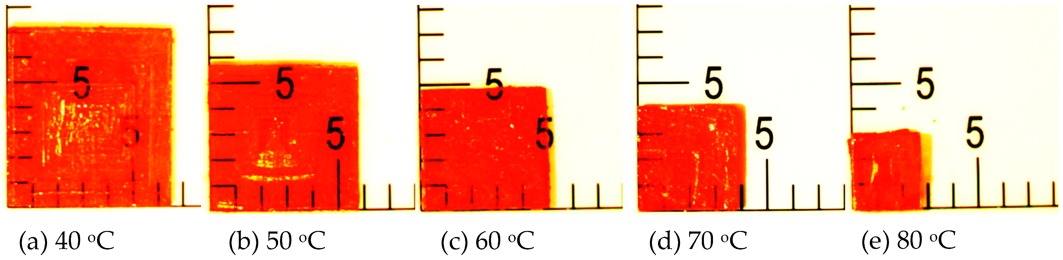
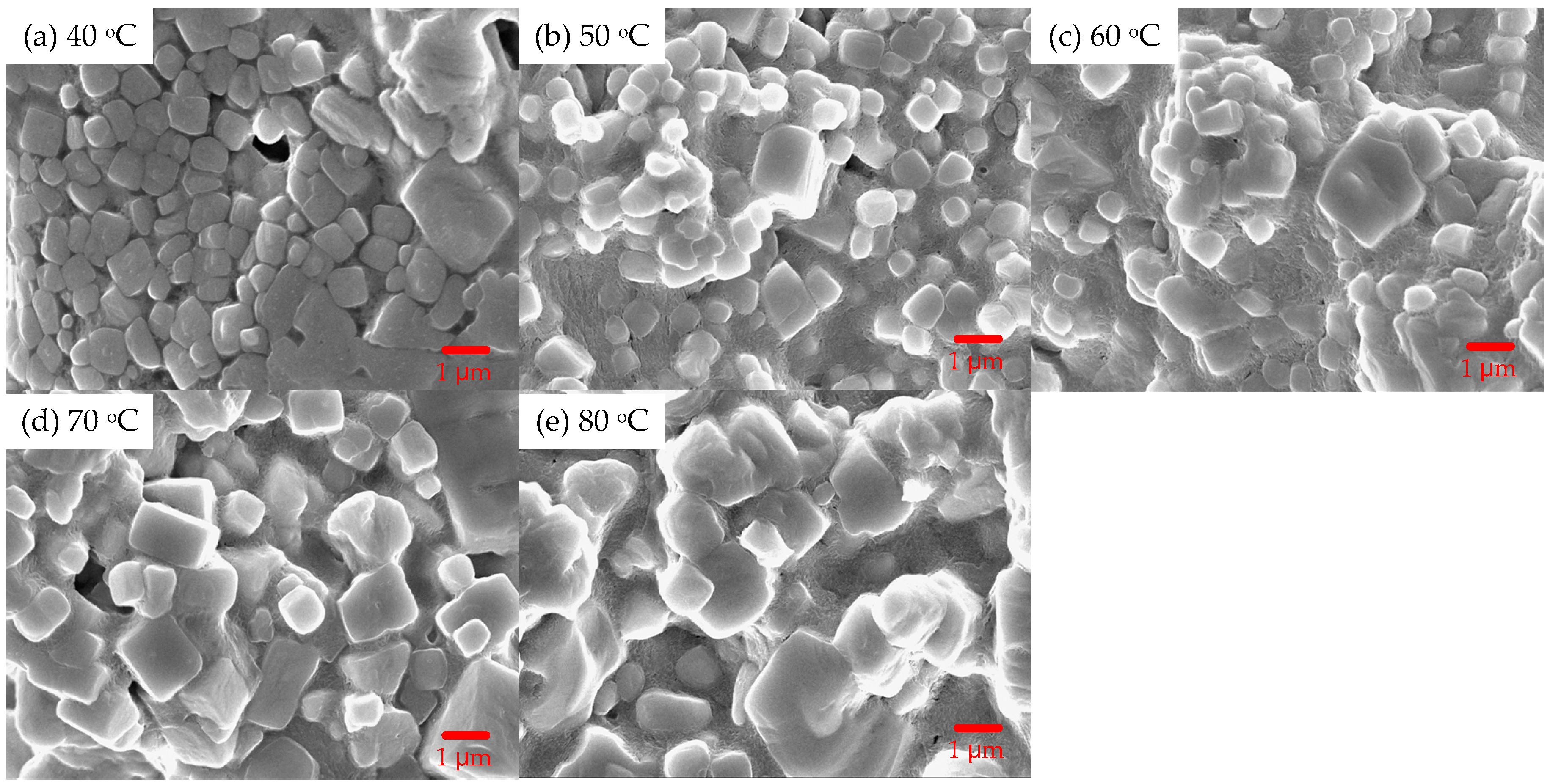
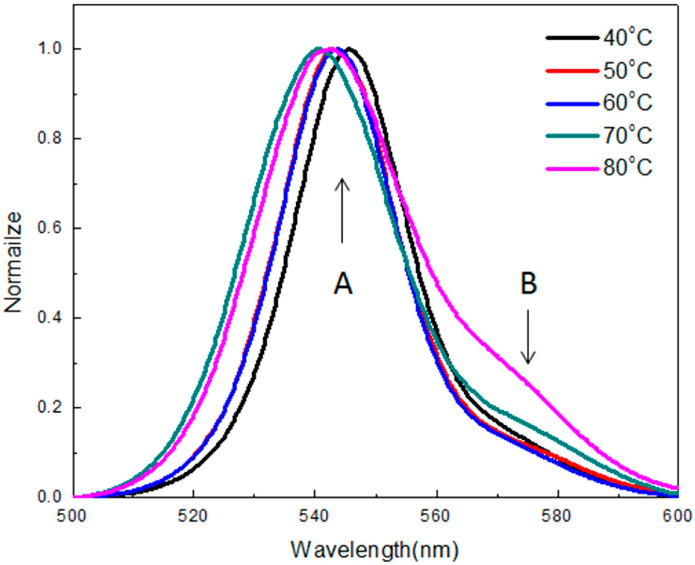
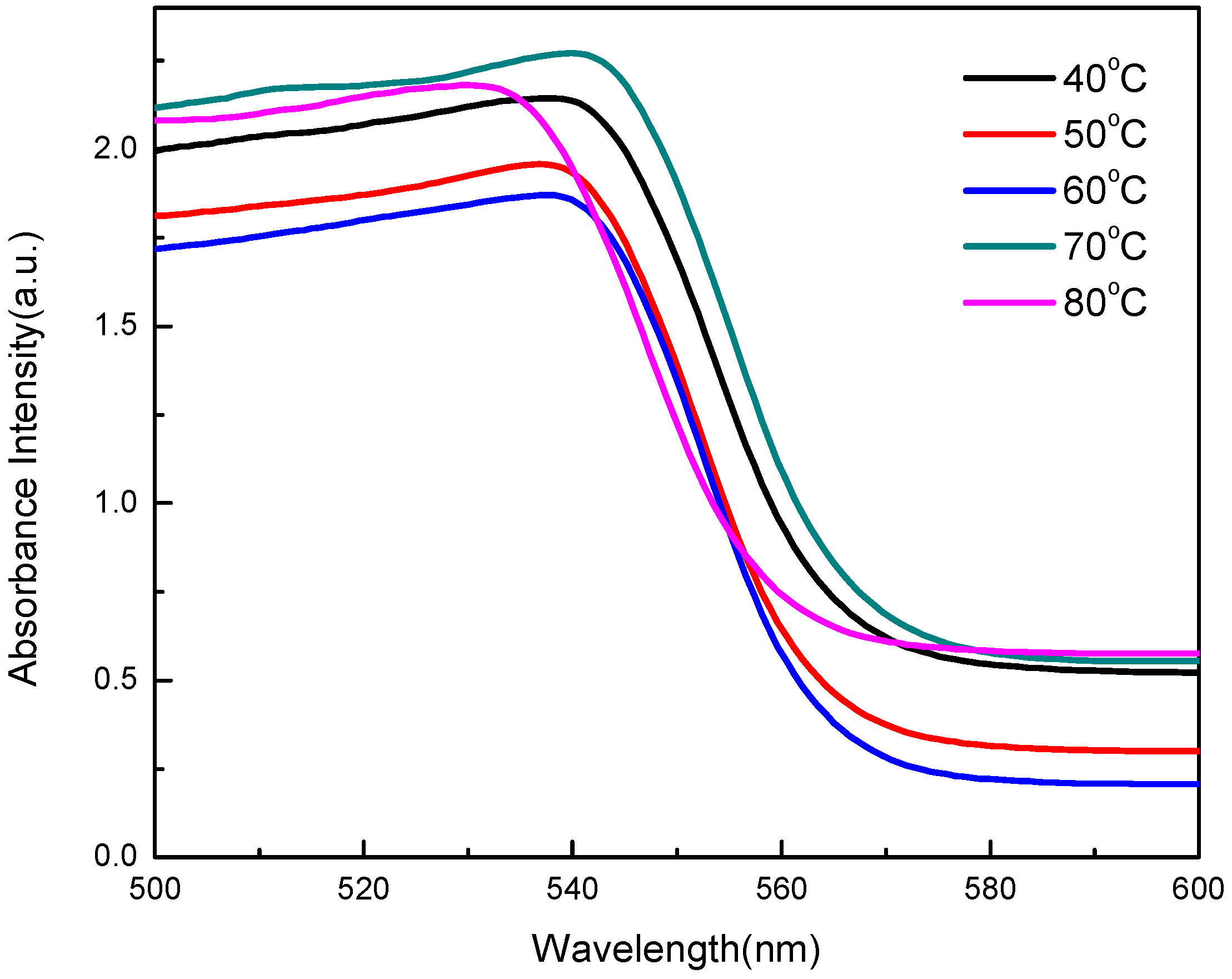
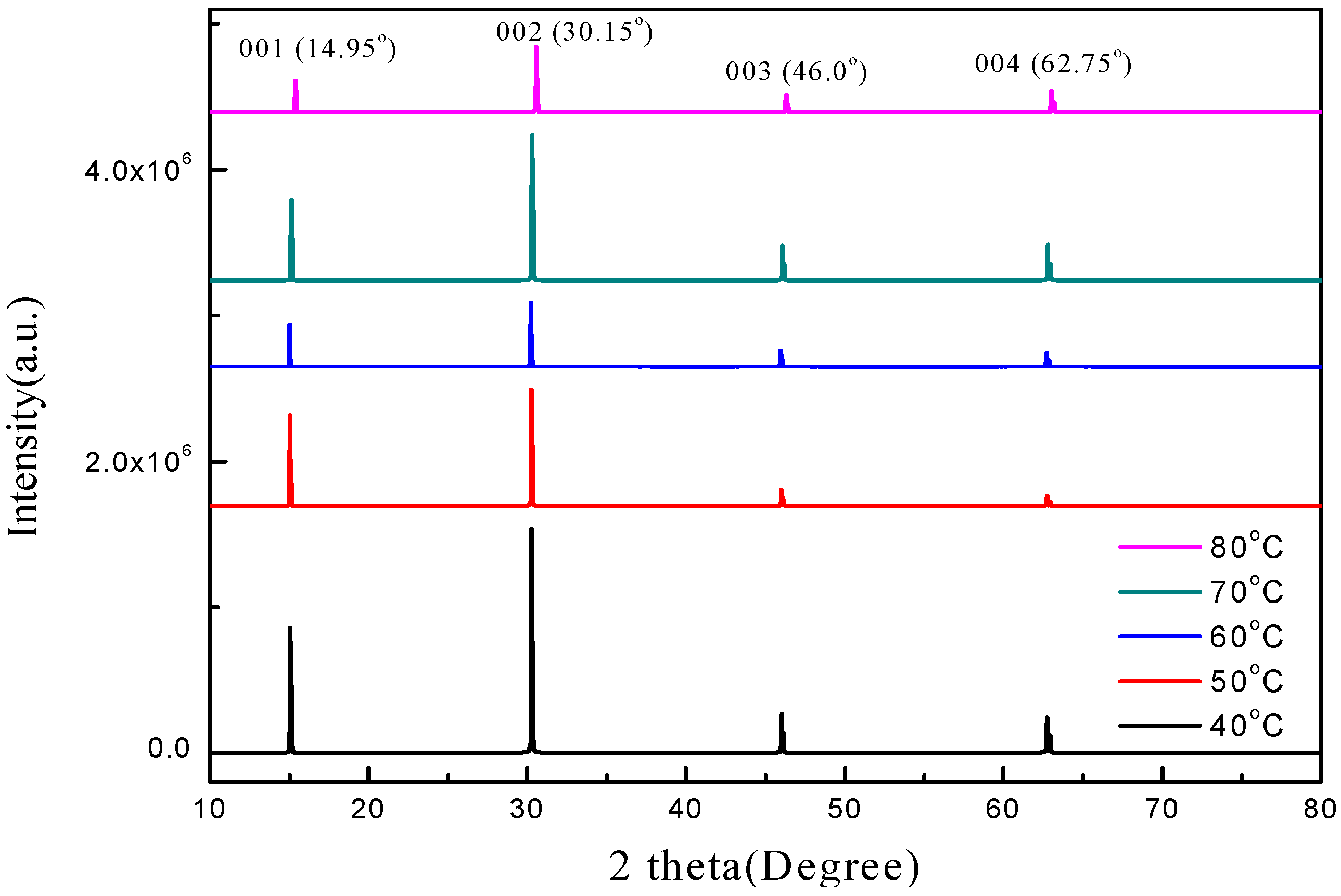
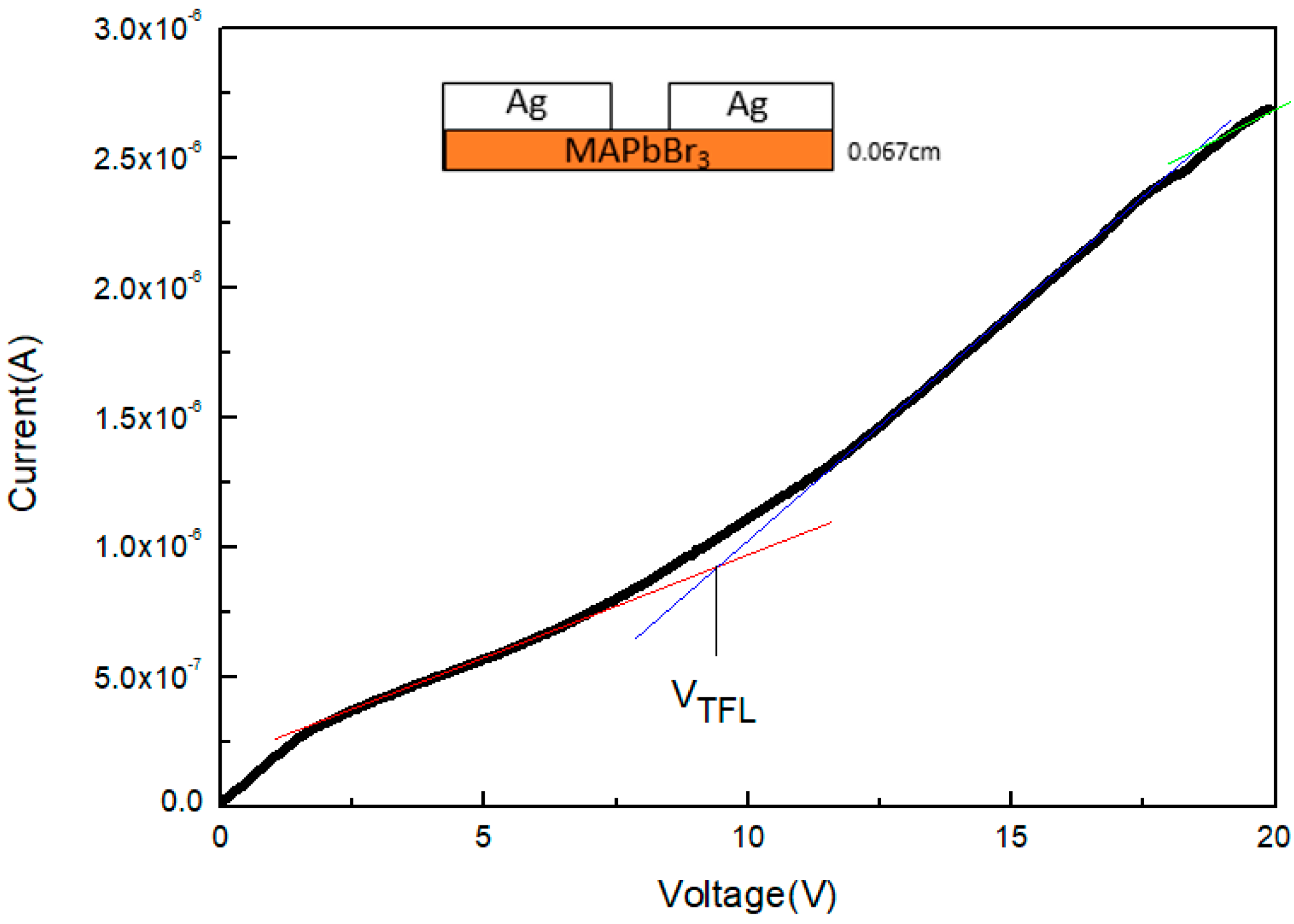
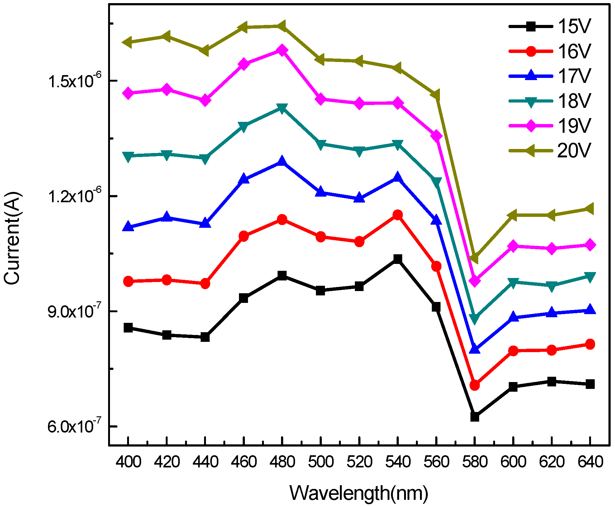
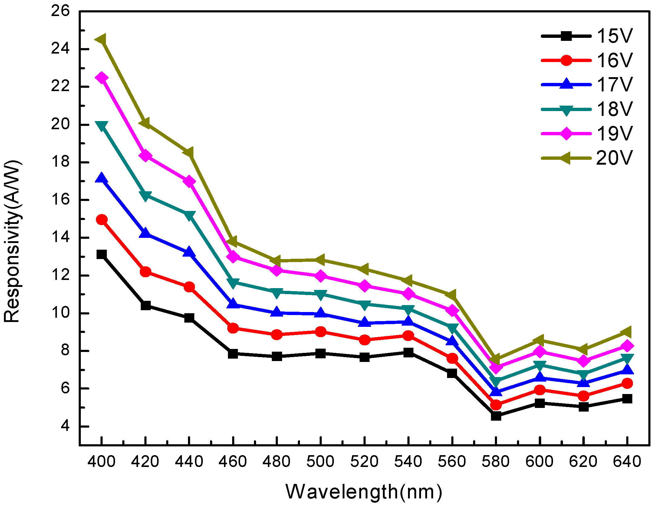
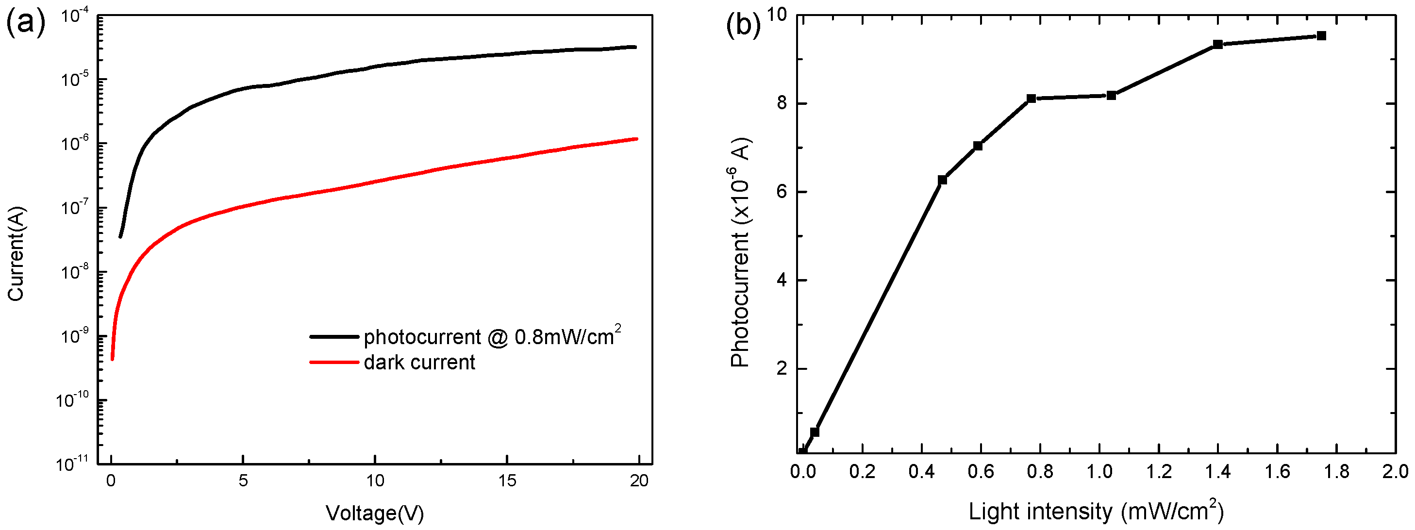
3. Results and Discussion

In this study, the CH3NH3PbBr3 precursor solution was grown in an oven until the solution completely evaporated. As shown in Figure 2, the CH3NH3PbBr3 crystal size was the largest under the growth temperature at 40 °C (45.5 mm2). However, the MAPbBr3 crystal area gradually decreased with an increase in the growth temperature. The CH3NH3PbBr3 crystal area was the smallest under the growth temperature at 80 °C (9 mm2). Therefore, it can be observed that the growth temperature is inversely proportional to the crystal size. A high temperature makes the solution evaporate and decrease, such that it is difficult to grow a large-sized crystal.
Figure 3 shows the scanning electron microscopy (SEM) images of the MAPbBr3 crystals at 40 °C, 50 °C, 60 °C, 70 °C, and 80 °C, respectively.
The MAPbBr3 crystal was composed of several crystal grains. The crystal obtained at 40 and 80 °C comprised many smaller and larger grains, respectively. Further, it was found that the crystal grains constituting the MAPbBr3 crystals became larger with an increase in the growth temperature.
As shown in Figure 4, the photoluminescence (PL) emission peaks of MAPbBr3 crystals were located at 545.6 nm, 543 nm, 543.6 nm, 540.6 nm, and 542.4 nm at temperatures of 40 °C, 50 °C, 60 °C, 70 °C, and 80 °C, respectively. It was observed that the peaks were in close proximity between 540 nm and 546 nm. The PL emission peak exhibited a blue shift with an increase in the growth temperature. The blue shift may be attributed to the difference in laser fluence and measurement system, as well as the atmosphere environment for characterization. [29,30,31]. The dominant PL peak (peak A) with the highest energy is located at ~545 nm (2.275 eV, close to band gap) with a full width at half maximum (FWHM) of ~30 nm. It is corresponding to the band-to-band transition. The lower energy peak (peak B) at ~560 nm, which had a broad bandwidth of 30 nm, was attributed to the emission of band-to-trap state (Br vacancies on the crystal surface) [32,33,34].
As shown in Figure 5, the edges of absorption spectra of the MAPbBr3 crystals were located at 537.58 nm, 536.83 nm, 537.58 nm, 539.85 nm, and 536.03 nm at temperatures of 40 °C, 50 °C, 60 °C, 70 °C, and 80 °C, respectively. It can be observed that the edges of absorption spectra are extremely close to one another, and that the peaks are located between 530 nm and 540 nm, corresponding to the band gap of 2.275 eV of MAPbBr3 single crystals [35].
Figure 6 shows the X-ray diffraction (XRD) patterns of the MAPbBr3 crystal at 40 °C, 50 °C, 60 °C, 70 °C, and 80 °C. All growth temperatures displayed significant peaks at 14.95°, 30.15°, 46.0°, and 62.75°. The crystal plane directions corresponding to the cubic crystal structure were (001), (002), (003), and (004), which, in turn, correspond to high-quality MAPbBr3 crystals. When the temperature was 40 °C, the peak intensity was observed to be higher. Conversely, at 80 °C, the peak intensities were significantly lower. It can be seen from the SEM images in Figure 2 that the crystallinity and density of the sample prepared at 40 °C is the best. The peak intensity is greater than that of the samples prepared at the temperatures of 50 to 80 °C, which is due to the lower density even though the particles are larger.
Figure 7 shows the current–voltage curve of the MAPbBr3 crystal; the red, blue, and green lines depict the Ohmic region (n = 1), trap-filled region (n > 3), and Child’s region (n = 2), respectively. According to Mott-Gurney’s law: μ = 8JDL3/9εεoV2 [26,36]. Consequently, the carrier mobility of the MAPbBr3 crystal was calculated to be 14.4 cm2V−1s−1. The trap density is calculated using the following equation: nt = 2VTFLεεo/eL2; the trap density of MAPbBr3 crystals was 4.7 × 1010 cm−3.
The MSM structure of the MAPbBr3 crystal photodetector is shown in Figure 8a. A medium layer C60 was inserted between the silver (Ag) electrodes and the MAPbBr3 crystal in order to prevent from a compound of both. Figure 8b shows a photograph of the MAPbBr3 crystal with the MSM structure.
Figure 9 shows the current vs. wavelength graph of the photodetector under each bias. The devices exhibit high current values in the wavelength range of 400 nm to 560 nm for each bias. However, the current decreased significantly in the range of 570 nm to 580 nm. The absorption edge located at around 580 nm is corresponding to the trap level transition. The current was observed to rise slightly between 600 nm and 640 nm owing to the carrier relations from the trap in the band structure.
Figure 10 shows the wavelength and responsivity at different bias voltages. At a wavelength of 400 nm, the responsivity of the component is 13.13 A/W, 14.97 A/W, 17.13 A/W, 19.98 A/W, 22.48 A/W, and 24.50 A/W at different bias voltages of 15 V, 16 V, 17 V, 18 V, 19 V, and 20 V, respectively. From 400 nm to 460 nm, the responsivity gradually decreases and becomes stable in the range of 460 nm to 560 nm. The responsivity attained its lowest value at 580 nm, and increases slightly in the range of 600 nm to 640 nm.
Figure 11a plots typical dark and illuminated (under 0.8 mW/cm2) I–V characteristics of MSM-MAPbBr3 crystal photodetectors at a bias ranging from 0 to 20 V. The photocurrent was approximately 7.04 × 10⁻⁶ A, and the dark current was approximately 1.04 × 10⁻⁷ A at a bias of 5 V. In this research, a relatively high dark current is a result of leakage current from the boundary in the crystal. However, a large photocurrent-to-dark-current contrast ratio is observed—at almost two orders of magnitude. The orders of magnitude of the photocurrent-to-dark-current contrast ratio were similar to other structures in other studies [37,38,39]. As shown in Figure 11b, the photocurrent density at −5 V was measured under different illumination intensities of a 200 W Xe lamp as the light source in order to study the dependence of the photocurrent on the incident light intensity. A linear relationship was observed when the intensity of incident light power was lower than 0.8 mW/cm2. However, when the light intensity was higher than 0.8 mW/cm2, the photocurrent was saturated owing to the balance between generation and recombination of electron–hole pairs.

4. Conclusions

In this study, MAPbBr3 crystals were grown at low temperatures using an improved inverse temperature crystallization method. It was observed that the small single crystals obtained at different growth temperatures became larger as the temperature increased; however, the crystal size was found to decrease as the temperature increased. In all single crystals, the sample prepared at temperature 80 °C showed the smallest size; the single crystal prepared at 40 °C was observed to have the largest size. The XRD pattern revealed four significantly high peaks, which were associated with high-quality MAPbBr3 crystals. The PL emission peak was obtained between 536 nm to 538 nm. The absorption edge was located at 580 nm and corresponded to the trap-level transition. The photocurrent increased slightly from 600 to 640 nm, which had been caused by the carrier relations from the trap level.

Author Contributions

L.-C.C. wrote the paper and designed the experiments. L.-C.C., K.-Y.L., and R.-M.L. analyzed the data. K.-L.L. and Y.-W.H. prepared the samples and performed all measurements. All authors have read and agreed to the published version of the manuscript.

Funding

This research was funded by the Ministry of Science and Technology of the Republic of China, grant number MOST 108-2211-E-027-093.

Conflicts of Interest

The authors declare no conflict of interest.

References

  1. Hata, T.; Giorgi, G.; Yamashita, K.; Caddeo, C.; Mattoni, A. Development of a Classical Interatomic Potential for MAPbBr3. J. Phys. Chem. C 2017, 121, 3724–3733. [Google Scholar] [CrossRef]
  2. Chen, H.; Zheng, X.; Li, Q.; Yang, Y.; Xiao, S.; Hu, C.; Bai, Y.; Zhang, T.; Wong, K.S.; Yang, S. An amorphous precursor route to the conformable oriented crystallization of CH3NH3PbBr3 in mesoporous scaffolds: Toward efficient and thermally stable carbon-based perovskite solar cells. J. Mater. Chem. A 2016, 4, 12897–12912. [Google Scholar] [CrossRef]
  3. Deschler, F.; Price, M.; Pathak, S.; Klintberg, L.E.; Jarausch, D.D.; Higler, R.; Hüttner, S.; Leijtens, T.; Stranks, S.D.; Snaith, H.J.; et al. High Photoluminescence Efficiency and Optically Pumped Lasing in Solution-Processed Mixed Halide Perovskite Semiconductors. J. Phys. Chem. Lett. 2014, 5, 1421–1426. [Google Scholar] [CrossRef] [PubMed]
  4. Wang, H.C.; Wang, W.; Tang, A.C.; Tsai, H.Y.; Bao, Z.; Ihara, T.; Yarita, N.; Tahara, H.; Kanemitsu, Y.; Chen, S.; et al. High-Performance CsPb1-xSnxBr3 Perovskite Quantum Dots for Light-Emitting Diodes. Angew. Chem. Int. Ed. Engl. 2017, 56, 13650–13654. [Google Scholar] [CrossRef] [PubMed]
  5. Cho, H.; Kim, J.S.; Yun, H.J.; Bae, J.S.; Heo, J.; Ahn, S.; Lee, T.; Wolf, C. High-Efficiency Solution-Processed Inorganic Metal Halide Perovskite Light-Emitting Diodes. Adv. Mater. 2017, 29, 1700579. [Google Scholar] [CrossRef]
  6. Li, J.; Xu, L.; Wang, T.; Song, J.; Chen, J.; Xue, J.; Dong, Y.; Cai, B.; Shan, Q.; Han, B.; et al. 50-Fold EQE Improvement up to 6.27% of Solution-Processed All-Inorganic Perovskite CsPbBr3 QLEDs via Surface Ligand Density Control. Adv. Mater. 2017, 29, 1603885. [Google Scholar] [CrossRef]
  7. Zhu, Z.; Zhao, D.; Chueh, C.C.; Shi, X.; Li, Z.; Jen, A.K.Y. Highly Efficient and Stable Perovskite Solar Cells Enabled by All-Crosslinked Charge-Transporting Layers. Joule 2018, 2, 168–183. [Google Scholar] [CrossRef] [Green Version]
  8. Yang, W.S.; Park, B.W.; Jung, E.H.; Jeon, N.J.; Kim, Y.C.; Lee, D.U.; Shin, S.S.; Seo, J.; Kim, E.K.; Noh, J.H.; et al. Iodide management in formamidinium-lead-halide–based perovskite layers for efficient solar cells. Science 2017, 356, 1376–1379. [Google Scholar] [CrossRef] [Green Version]
  9. Cai, M.; Ishida, N.; Li, X.; Yang, X.; Noda, T.; Wu, Y.; Xie, F.; Naito, H.; Fujita, D.; Han, L. Control of Electrical Potential Distribution for High-Performance Perovskite Solar Cells. Joule 2018, 2, 296–306. [Google Scholar] [CrossRef] [Green Version]
  10. McMeekin, D.P.; Sadoughi, G.; Rehman, W.; Eperon, G.E.; Saliba, M.; Hörantner, M.T.; Haghighirad, A.; Sakai, N.; Korte, L.; Rech, B.; et al. A mixed-cation lead mixed-halide perovskite absorber for tandem solar cells. Science 2016, 351, 151–155. [Google Scholar] [CrossRef] [Green Version]
  11. Chen, Z.; Dong, Q.; Liu, Y.; Bao, C.; Fang, Y.; Lin, Y.; Tang, S.; Wang, Q.; Xiao, X.; Bai, Y.; et al. Thin single crystal perovskite solar cells to harvest below-bandgap light absorption. Nat. Commun. 2017, 8, 1890. [Google Scholar] [CrossRef] [PubMed] [Green Version]
  12. Bao, C.; Chen, Z.; Fang, Y.; Wei, H.; Deng, Y.; Xiao, X.; Li, L.; Huang, J. Low-Noise and Large-Linear-Dynamic-Range Photodetectors Based on Hybrid-Perovskite Thin-Single-Crystals. Adv. Mater. 2017, 29, 1703209. [Google Scholar] [CrossRef] [PubMed]
  13. Wei, H.; Fang, Y.; Mulligan, P.; Chuirazzi, W.; Fang, H.H.; Wang, C.; Ecker, B.R.; Gao, Y.; Loi, M.A.; Cao, L.; et al. Sensitive X-ray detectors made of methylammonium lead tribromide perovskite single crystals. Nat. Photonics 2016, 10, 333–339. [Google Scholar] [CrossRef]
  14. Saidaminov, M.I.; Adinolfi, V.; Comin, R.; Abdelhady, A.L.; Peng, W.; Dursun, I.; Yuan, M.; Hoogland, S.; Sargent, E.H.; Bakr, O.M. Planar-integrated single-crystalline perovskite photodetectors. Nat. Commun. 2015, 6, 8724. [Google Scholar] [CrossRef] [PubMed] [Green Version]
  15. Liu, Y.; Zhang, Y.; Yang, Z.; Yang, N.; Ren, X.; Pang, L.; Liu, S.F. Thinness- and Shape-Controlled Growth for Ultrathin Single-Crystalline Perovskite Wafers for Mass Production of Superior Photoelectronic Devices. Adv. Mater. 2016, 28, 9204–9209. [Google Scholar] [CrossRef]
  16. Gao, L.; Zeng, K.; Guo, J.; Ge, C.; Du, J.; Zhao, Y.; Chen, C.; Deng, H.; He, Y.; Song, H.; et al. Passivated Single-Crystalline CH3NH3PbI3 Nanowire Photodetector with High Detectivity and Polarization Sensitivity. Nano Lett. 2016, 16, 7446–7454. [Google Scholar] [CrossRef]
  17. Chandrasekar, P.V.; Yang, S.; Hu, J.; Sulaman, M.; Shi, Y.; Saleem, M.I.; Tang, Y.; Jiang, Y.; Zou, B.; Muhammad, I.S. Solution-phase, template-free synthesis of PbI2 and MAPbI3 nano/microtubes for high-sensitivity photodetectors. Nanoscale 2019, 11, 5188–5196. [Google Scholar] [CrossRef]
  18. Chen, L.C.; Weng, C.Y. Optoelectronic Properties of MAPbI3 Perovskite/Titanium Dioxide Heterostructures on Porous Silicon Substrates for Cyan Sensor Applications. Nanoscale Res. Lett. 2015, 10, 404. [Google Scholar] [CrossRef] [Green Version]
  19. Yalcin, M.; Ozmen, D.; Yakuphanoglu, F. Perovskite cobaltates/p-silicon heterojunction photodiodes. J. Alloys Compd. 2019, 796, 243–254. [Google Scholar] [CrossRef]
  20. Tian, C.; Wang, F.; Wang, Y.; Yang, Z.; Chen, X.; Mei, J.; Liu, H.; Zhao, D. Chemical Vapor Deposition Method Grown All-Inorganic Perovskite Microcrystals for Self-Powered Photodetectors. ACS Appl. Mater. Interfaces 2019, 11, 15804–15812. [Google Scholar] [CrossRef]
  21. Cifci, O.S.; Koçyiğit, A.; Sun, P. Perovskite/p-Si photodiode with ultra-thin metal cathode. Superlattices Microstruct. 2018, 120, 492–500. [Google Scholar] [CrossRef]
  22. Luo, W.; Yan, L.; Liu, R.; Zou, T.; Zhang, S.; Liu, C.; Dai, Q.; Chen, J.; Zhou, H. High detectivity ITO/organolead halide perovskite Schottky photodiodes. Semicond. Sci. Technol. 2019, 34, 074004. [Google Scholar] [CrossRef]
  23. Pandey, K.; Chauhan, M.; Bhatt, V.; Tripathi, B.; Yadav, P.; Kumar, M. High-performance self-powered perovskite photodetector with a rapid photoconductive response. RSC Adv. 2016, 6, 105076–105080. [Google Scholar] [CrossRef]
  24. Lee, W.; Lee, J.; Yun, H.; Kim, J.; Park, J.; Choi, C.; Kim, D.C.; Seo, H.; Lee, H.; Yu, J.W.; et al. High-Resolution Spin-on-Patterning of Perovskite Thin Films for a Multiplexed Image Sensor Array. Adv. Mater. 2017, 29, 1702902. [Google Scholar] [CrossRef] [PubMed]
  25. Liu, Z.; Li, H.; Qin, C.; Zhang, T.; Gu, Y.; Chen, H.; Zheng, H.; Li, S. Solution-Processed Inorganic Perovskite Flexible Photodetectors with High Performance. Nanoscale Res. Lett. 2019, 14, 284. [Google Scholar] [CrossRef] [PubMed]
  26. Maculan, G.; Sheikh, A.D.; Abdelhady, A.L.; Saidaminov, M.I.; Haque, A.; Murali, B.; Alarousu, E.; Mohammed, O.F.; Wu, T.; Bakr, O.M. CH3NH3PbCl3 Single Crystals: Inverse Temperature Crystallization and Visible-Blind UV-Photodetector. J. Phys. Chem. Lett. 2015, 6, 3781–3786. [Google Scholar] [CrossRef] [Green Version]
  27. Dang, Y.; Liu, Y.; Sun, Y.; Yuan, D.; Liu, X.; Lu, W.; Liu, G.; Xia, H.; Tao, X. Bulk crystal growth of hybrid perovskite material CH3NH3PbI3. CrystEngComm 2015, 17, 665–670. [Google Scholar] [CrossRef]
  28. Shi, D.; Adinolfi, V.; Comin, R.; Yuan, M.; Alarousu, E.; Buin, A.; Chen, Y.; Hoogland, S.; Rothenberger, A.; Katsiev, K.; et al. Low trap-state density and long carrier diffusion in organolead trihalide perovskite single crystals. Science 2015, 347, 519–522. [Google Scholar] [CrossRef] [Green Version]
  29. Fang, H.H.; Adjokatse, S.; Wei, H.; Yang, J.; Blake, G.R.; Huang, J.; Even, J.; Loi, M.A. Ultrahigh sensitivity of methylammonium lead tribromide perovskite single crystals to environmental gases. Sci. Adv. 2016, 2, e1600534. [Google Scholar] [CrossRef] [Green Version]
  30. Qiu, Y.H.; Nan, F.; Wang, Q.; Liu, X.D.; Ding, S.J.; Hao, Z.H.; Zhou, L.; Wang, Q.Q. Tuning the Competitive Recombination of Free Carriers and Bound Excitons in Perovskite CH3NH3PbBr3 Single Crystal. J. Phys. Chem. C 2017, 121, 6916. [Google Scholar] [CrossRef]
  31. Murali, B.; Dey, S.; Abdelhady, A.L.; Peng, W.; Alarousu, E.; Kirmani, A.R.; Cho, N.; Sarmah, S.P.; Parida, M.R.; Saidaminov, M.I.; et al. Surface restructuring of hybrid perovskite crystals. ACS Energy Lett. 2016, 1, 1119. [Google Scholar] [CrossRef] [Green Version]
  32. Wu, X.; Trinh, M.T.; Niesner, D.; Zhu, H.; Norman, Z.; Owen, J.S.; Yaffe, O.; Kudisch, B.J.; Zhu, X.Y. Trap States in Lead Iodide Perovskites. J. Am. Chem. Soc. 2015, 137, 2089–2096. [Google Scholar] [CrossRef] [PubMed]
  33. Mante, P.A.; Stoumpos, C.C.; Kanatzidis, M.G.; Yartsev, A. Electron–acoustic phonon coupling in single crystal CH3NH3PbI3 perovskites revealed by coherent acoustic phonons. Nat. Commun. 2017, 8, 14398. [Google Scholar] [CrossRef] [PubMed]
  34. Wu, K.; Bera, A.; Ma, C.; Du, Y.; Yang, Y.; Li, L.; Wu, T. Temperature-dependent excitonic photoluminescence of hybrid organometal halide perovskite films. Phys. Chem. Chem. Phys. 2014, 16, 22476–22481. [Google Scholar] [CrossRef] [PubMed]
  35. Han, L.; Liu, C.; Wu, L.; Zhang, J. Observation of the growth of MAPbBr3 single-crystalline thin film based on space-limited method. J. Cryst. Growth 2018, 501, 27–33. [Google Scholar] [CrossRef]
  36. Chen, L.C.; Lee, K.L.; Lin, S.E. Observation of Hybrid MAPbBr3 Perovskite Bulk Crystals Grown by Repeated Crystallizations. Crystals 2018, 8, 260. [Google Scholar] [CrossRef] [Green Version]
  37. Liu, C.; Wang, K.; Yi, C.; Shi, X.; Du, P.; Smith, A.W.; Karim, A.; Gong, X. Ultrasensitive solution-processed perovskite hybrid photodetectors. J. Mater. Chem. C 2015, 3, 6600–6606. [Google Scholar] [CrossRef]
  38. Lee, S.W.; Choi, K.J.; Kang, B.H.; Lee, J.S.; Kim, S.W.; Kwon, J.B.; Gopalan, S.A.; Bae, J.H.; Kim, E.S.; Kwon, D.H.; et al. Low dark current and improved detectivity of hybrid ultraviolet photodetector based on carbon-quantum-dots/zinc-oxide-nanorod composites. Org. Electron. 2016, 39, 250–257. [Google Scholar] [CrossRef]
  39. Lee, S.W.; Cha, S.H.; Choi, K.J.; Kang, B.H.; Lee, J.S.; Kim, S.W.; Kim, J.S.; Jeong, H.M.; Gopalan, S.A.; Kwon, D.H.; et al. Low Dark-Current, High Current-Gain of PVK/ZnO Nanoparticles Composite-Based UV Photodetector by PN-Heterojunction Control. Sensors 2016, 16, 74. [Google Scholar] [CrossRef] [Green Version]
Figure 1. Schematic diagram of experimental procedure in this research.
Sensors 20 00297 g001
Figure 2. Pictures of MAPbBr3 crystals prepared at various temperature. The unit of scale is 1 mm.
Sensors 20 00297 g002
Figure 3. Scanning electron microscopy (SEM) images of the MAPbBr3 crystals growth temperature at (a) 40 °C, (b) 50 °C, (c) 60 °C, (d) 70 °C, and (e) 80 °C.
Sensors 20 00297 g003
Figure 4. Photoluminescence (PL) spectra of the MAPbBr3 crystals prepared at various temperatures.
Sensors 20 00297 g004
Figure 5. Absorption spectra of the MAPbBr3 crystals prepared at various temperatures.
Sensors 20 00297 g005
Figure 6. X-ray diffraction (XRD) patterns of the MAPbBr3 crystals prepared at various temperatures.
Sensors 20 00297 g006
Figure 7. Current–voltage curve of the MAPbBr3 crystal.
Sensors 20 00297 g007
Figure 8. (a) Metal–semiconductor–metal (MSM) structure of the MAPbBr3 crystal photodetector. (b) Photograph of a MAPbBr3 crystal photodetector.
Sensors 20 00297 g008
Figure 9. Current and wavelength curve MSM-MAPbBr3 crystal photodetectors.
Sensors 20 00297 g009
Figure 10. Responsivity and wavelength curve of MSM-MAPbBr3 crystal photodetectors.
Sensors 20 00297 g010
Figure 11. (a) Current–Voltage (I–V) characteristics and (b) dynamic range of the MSM-MAPbBr3 crystal photodetector under illumination of 0.8 mW/cm2 and measured at 5 V.
Sensors 20 00297 g011

