
Dual-Dewetting Process for Self-Assembled Nanoparticle Clusters in Wafer Scale
 ,
,  , , , and
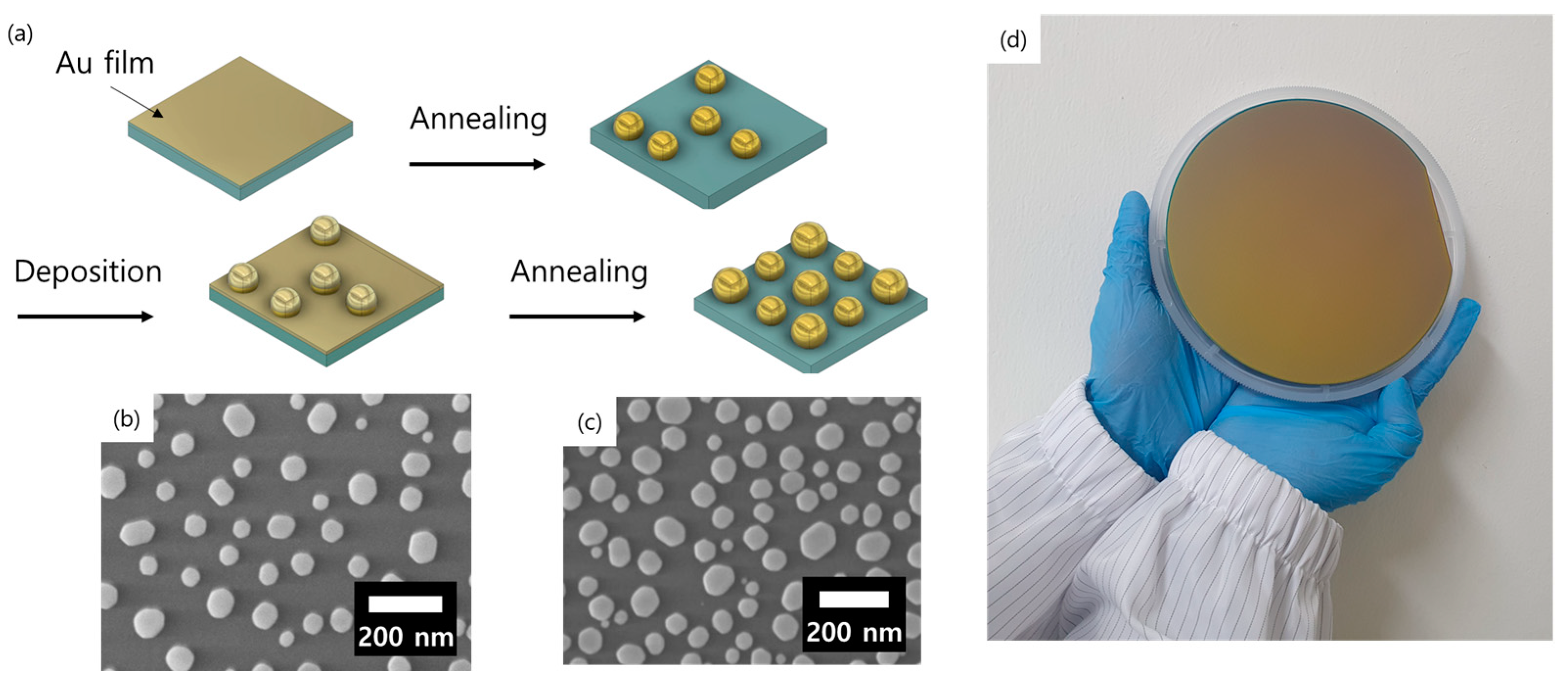
Abstract
:1. Introduction
2. Results and Discussion
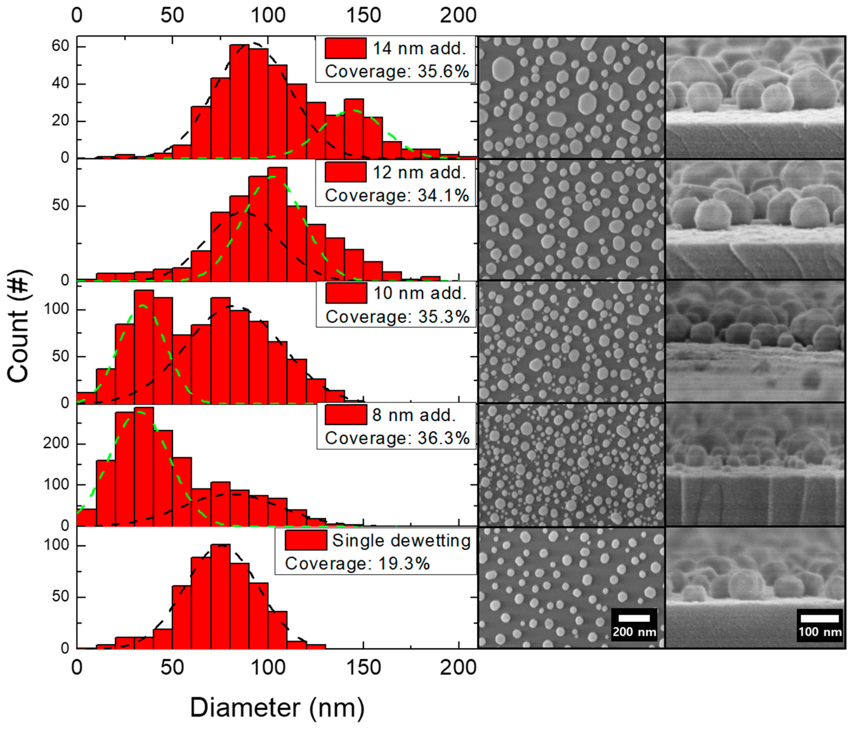
2.1. Subsection Shape and Distribution Characteristics of Gold Nanoparticles by Dewetting
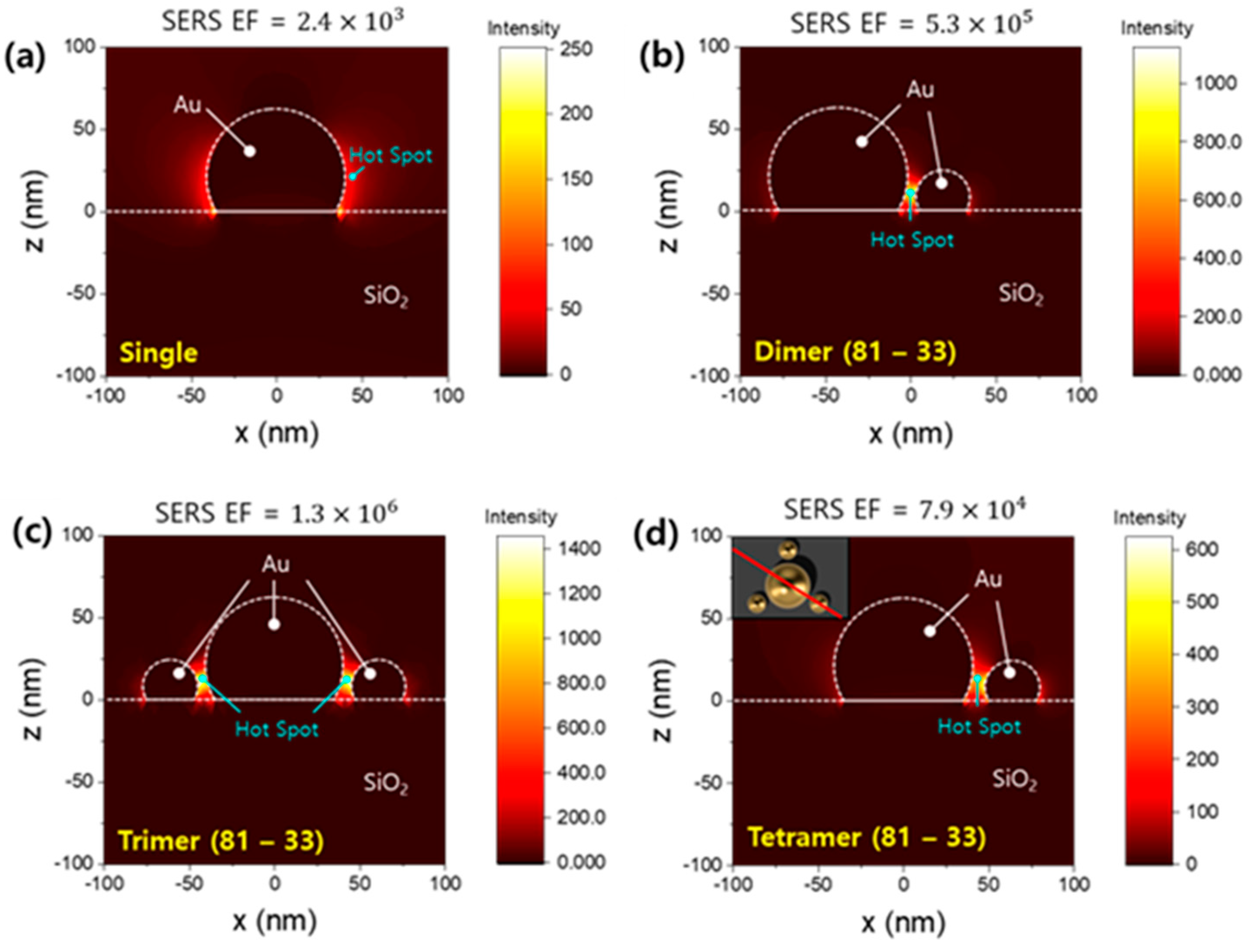
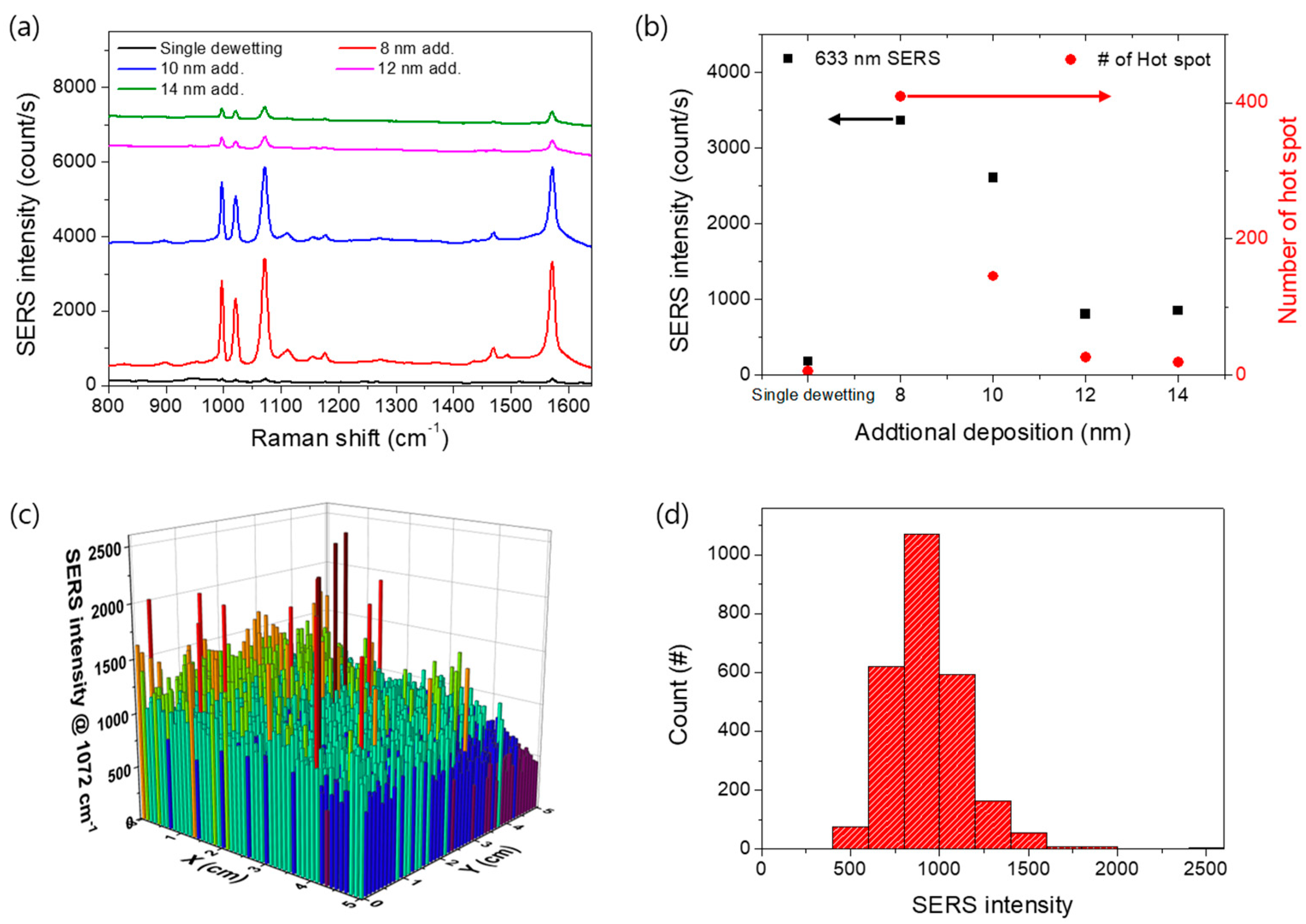
2.2. Enhancement of Dual-Dewetted Gold Nanoparticles Tics of Gold Nanoparticles by Dewetting
3. Materials and Methods
3.1. Dual-Dewetting Gold Nanoparticle Substrate Fabrication
3.2. Simulation
3.3. SERS Measurement
4. Conclusions
Supplementary Materials
Author Contributions
Funding
Institutional Review Board Statement
Informed Consent Statement
Data Availability Statement
Conflicts of Interest
References
- Fan, J.A.; Wu, C.; Bao, K.; Bao, J.; Bardhan, R.; Halas, N.J.; Manoharan, V.N.; Nordlander, P.; Shvets, G.; Capasso, F. Self-assembled plasmonic nanoparticle clusters. Science 2010, 328, 1135–1138. [Google Scholar] [CrossRef] [PubMed]
- Haran, G.; Chuntonov, L. Artificial plasmonic molecules and their interaction with real molecules. Chem. Rev. 2018, 118, 5539–5580. [Google Scholar] [CrossRef] [PubMed]
- Fleetham, T.; Choi, J.-Y.; Choi, H.W.; Alford, T.; Jeong, D.S.; Lee, T.S.; Lee, W.S.; Lee, K.-S.; Li, J.; Kim, I. Photocurrent enhancements of organic solar cells by altering dewetting of plasmonic Ag nanoparticles. Sci. Rep. 2015, 5, 14250. [Google Scholar] [CrossRef] [PubMed]
- Atwater, H.A.; Polman, A. Plasmonics for improved photovoltaic devices. Nat. Mater. 2010, 9, 205–213. [Google Scholar] [CrossRef]
- Ferry, V.E.; Munday, J.N.; Atwater, H.A. Design considerations for plasmonic photovoltaics. Adv. Mater. 2010, 22, 4794–4808. [Google Scholar] [CrossRef]
- Zang, F.; Su, Z.; Zhou, L.; Konduru, K.; Kaplan, G.; Chou, S.Y. Ultrasensitive Ebola virus antigen sensing via 3D nanoantenna arrays. Adv. Mater. 2019, 31, 1902331. [Google Scholar] [CrossRef]
- Tabakman, S.M.; Chen, Z.; Casalongue, H.S.; Wang, H.; Dai, H. A New Approach to Solution-Phase Gold Seeding for SERS Substrates. Small 2011, 7, 499–505. [Google Scholar] [CrossRef]
- Adhikari, S.; Ampadu, E.K.; Kim, M.; Noh, D.; Oh, E.; Lee, D. Detection of explosives by SERS platform using metal nanogap substrates. Sensors 2021, 21, 5567. [Google Scholar] [CrossRef]
- Li, W.-D.; Ding, F.; Hu, J.; Chou, S.Y. Three-dimensional cavity nanoantenna coupled plasmonic nanodots for ultrahigh and uniform surface-enhanced Raman scattering over large area. Opt. Express 2011, 19, 3925–3936. [Google Scholar] [CrossRef]
- Caldwell, J.D.; Glembocki, O.; Bezares, F.J.; Bassim, N.D.; Rendell, R.W.; Feygelson, M.; Ukaegbu, M.; Kasica, R.; Shirey, L.; Hosten, C. Plasmonic nanopillar arrays for large-area, high-enhancement surface-enhanced Raman scattering sensors. ACS Nano 2011, 5, 4046–4055. [Google Scholar] [CrossRef]
- Oh, Y.J.; Jeong, K.H. Glass Nanopillar Arrays with Nanogap-Rich Silver Nanoislands for Highly Intense Surface Enhanced Raman Scattering. Adv. Mater. 2012, 24, 2234–2237. [Google Scholar] [CrossRef] [PubMed]
- Park, H.J.; Cho, S.; Kim, M.; Jung, Y.S. Carboxylic acid-functionalized, graphitic layer-coated three-dimensional SERS substrate for label-free analysis of Alzheimer’s disease biomarkers. Nano Lett. 2020, 20, 2576–2584. [Google Scholar] [CrossRef] [PubMed]
- Linh, V.T.N.; Lee, M.-Y.; Mun, J.; Kim, Y.; Kim, H.; Han, I.W.; Park, S.-G.; Choi, S.; Kim, D.-H.; Rho, J. 3D plasmonic coral nanoarchitecture paper for label-free human urine sensing and deep learning-assisted cancer screening. Biosens. Bioelectron. 2023, 224, 115076. [Google Scholar] [CrossRef] [PubMed]
- Cinel, N.A.; Cakmakyapan, S.; Butun, S.; Ertas, G.; Ozbay, E. E-Beam lithography designed substrates for surface enhanced Raman spectroscopy. Photonics Nanostruct.-Fundam. Appl. 2015, 15, 109–115. [Google Scholar] [CrossRef]
- Yue, W.; Wang, Z.; Yang, Y.; Chen, L.; Syed, A.; Wong, K.; Wang, X. Electron-beam lithography of gold nanostructures for surface-enhanced Raman scattering. J. Micromech. Microeng. 2012, 22, 125007. [Google Scholar] [CrossRef]
- Joshi, R.; Adhikari, S.; Son, J.P.; Jang, Y.; Lee, D.; Cho, B.-K. Au nanogap SERS substrate for the carbaryl pesticide determination in juice and milk using chemomterics. Spectrochim. Acta Part A Mol. Biomol. Spectrosc. 2023, 297, 122734. [Google Scholar] [CrossRef] [PubMed]
- Halvorson, R.A.; Vikesland, P.J. Surface-enhanced Raman spectroscopy (SERS) for environmental analyses. Environ. Sci. Technol. 2010, 44, 7749–7755. [Google Scholar] [CrossRef]
- Han, Q.; Zhang, C.; Gao, W.; Han, Z.; Liu, T.; Li, C.; Wang, Z.; He, E.; Zheng, H. Ag-Au alloy nanoparticles: Synthesis and in situ monitoring SERS of plasmonic catalysis. Sens. Actuators B Chem. 2016, 231, 609–614. [Google Scholar] [CrossRef]
- Ren, H.; Yang, J.-L.; Yang, W.-M.; Zhong, H.-L.; Lin, J.-S.; Radjenovic, P.M.; Sun, L.; Zhang, H.; Xu, J.; Tian, Z.-Q.; et al. Core–Shell–Satellite Plasmonic Photocatalyst for Broad-Spectrum Photocatalytic Water Splitting. ACS Mater. Lett. 2021, 3, 69–76. [Google Scholar] [CrossRef]
- Wang, H.; Brandl, D.W.; Nordlander, P.; Halas, N.J. Plasmonic Nanostructures: Artificial Molecules. Acc. Chem. Res. 2007, 40, 53–62. [Google Scholar] [CrossRef]
- Wu, L.-A.; Li, W.-E.; Lin, D.-Z.; Chen, Y.-F. Three-Dimensional SERS Substrates Formed with Plasmonic Core-Satellite Nanostructures. Sci. Rep. 2017, 7, 13066. [Google Scholar] [CrossRef] [PubMed]
- Petti, L.; Capasso, R.; Rippa, M.; Pannico, M.; La Manna, P.; Peluso, G.; Calarco, A.; Bobeico, E.; Musto, P. A plasmonic nanostructure fabricated by electron beam lithography as a sensitive and highly homogeneous SERS substrate for bio-sensing applications. Vib. Spectrosc. 2016, 82, 22–30. [Google Scholar] [CrossRef]
- Clarke, C.; Liu, D.; Wang, F.; Liu, Y.; Chen, C.; Ton-That, C.; Xu, X.; Jin, D. Large-scale dewetting assembly of gold nanoparticles for plasmonic enhanced upconversion nanoparticles. Nanoscale 2018, 10, 6270–6276. [Google Scholar] [CrossRef]
- Rao, C.; Luber, E.J.; Olsen, B.C.; Buriak, J.M. Plasmonic Stamps Fabricated by Gold Dewetting on PDMS for Catalyzing Hydrosilylation on Silicon Surfaces. ACS Appl. Nano Mater. 2019, 2, 3238–3245. [Google Scholar] [CrossRef]
- Günendi, M.C.; Tanyeli, İ.; Akgüç, G.B.; Bek, A.; Turan, R.; Gülseren, O. Understanding the plasmonic properties of dewetting formed Ag nanoparticles for large area solar cell applications. Opt. Express 2013, 21, 18344–18353. [Google Scholar] [CrossRef]
- Chung, T.; Lee, Y.; Ahn, M.-S.; Lee, W.; Bae, S.-I.; Hwang, C.S.H.; Jeong, K.-H. Nanoislands as plasmonic materials. Nanoscale 2019, 11, 8651–8664. [Google Scholar] [CrossRef]
- Oh, Y.; Lee, J.; Lee, M. Fabrication of Ag-Au bimetallic nanoparticles by laser-induced dewetting of bilayer films. Appl. Surf. Sci. 2018, 434, 1293–1299. [Google Scholar] [CrossRef]
- Devaraj, V.; Lee, J.-M.; Adhikari, S.; Kim, M.; Lee, D.; Oh, J.-W. A single bottom facet outperforms random multifacets in a nanoparticle-on-metallic-mirror system. Nanoscale 2020, 12, 22452–22461. [Google Scholar] [CrossRef]
- Kang, M.; Park, S.-G.; Jeong, K.-H. Repeated solid-state dewetting of thin gold films for nanogap-rich plasmonic nanoislands. Sci. Rep. 2015, 5, 14790. [Google Scholar] [CrossRef]
- Fusco, Z.; Bo, R.; Wang, Y.; Motta, N.; Chen, H.; Tricoli, A. Self-assembly of Au nano-islands with tuneable organized disorder for highly sensitive SERS. J. Mater. Chem. C 2019, 7, 6308–6316. [Google Scholar] [CrossRef]
- Ray, N.J.; Yoo, J.-H.; Baxamusa, S.; Nguyen, H.T.; Elhadj, S.; Feigenbaum, E. Tuning gold nanoparticle size with fixed interparticle spacing in large-scale arrays: Implications for plasmonics and nanoparticle etching masks. ACS Appl. Nano Mater. 2021, 4, 2733–2742. [Google Scholar] [CrossRef]
- Devaraj, V.; Lee, J.-M.; Oh, J.-W. Influence of cavity geometry towards plasmonic gap tolerance and respective near-field in nanoparticle-on-mirror. Curr. Appl. Phys. 2020, 20, 1335–1341. [Google Scholar] [CrossRef]
- Baumberg, J.J.; Aizpurua, J.; Mikkelsen, M.H.; Smith, D.R. Extreme nanophotonics from ultrathin metallic gaps. Nat. Mater. 2019, 18, 668–678. [Google Scholar] [CrossRef] [PubMed]
- Devaraj, V.; Choi, J.-W.; Lee, J.-M.; Oh, J.-W. An Accessible Integrated Nanoparticle in a Metallic Hole Structure for Efficient Plasmonic Applications. Materials 2022, 15, 792. [Google Scholar] [CrossRef]


Disclaimer/Publisher’s Note: The statements, opinions and data contained in all publications are solely those of the individual author(s) and contributor(s) and not of MDPI and/or the editor(s). MDPI and/or the editor(s) disclaim responsibility for any injury to people or property resulting from any ideas, methods, instructions or products referred to in the content. |
© 2023 by the authors. Licensee MDPI, Basel, Switzerland. This article is an open access article distributed under the terms and conditions of the Creative Commons Attribution (CC BY) license (https://creativecommons.org/licenses/by/4.0/).
Share and Cite
Kim, M.; Ahn, H.-J.; Silalahi, V.C.; Heo, D.; Adhikari, S.; Jang, Y.; Lee, J.; Lee, D. Dual-Dewetting Process for Self-Assembled Nanoparticle Clusters in Wafer Scale. Int. J. Mol. Sci. 2023, 24, 13102. https://doi.org/10.3390/ijms241713102
Kim M, Ahn H-J, Silalahi VC, Heo D, Adhikari S, Jang Y, Lee J, Lee D. Dual-Dewetting Process for Self-Assembled Nanoparticle Clusters in Wafer Scale. International Journal of Molecular Sciences. 2023; 24(17):13102. https://doi.org/10.3390/ijms241713102
Chicago/Turabian StyleKim, Minjun, Hyun-Ju Ahn, Vanna Chrismas Silalahi, Damun Heo, Samir Adhikari, Yudong Jang, Jongmin Lee, and Donghan Lee. 2023. "Dual-Dewetting Process for Self-Assembled Nanoparticle Clusters in Wafer Scale" International Journal of Molecular Sciences 24, no. 17: 13102. https://doi.org/10.3390/ijms241713102