
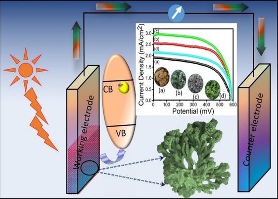
Impact of Annealing Temperature on the Morphological, Optical and Photoelectrochemical Properties of Cauliflower-like CdSe0.6Te0.4 Photoelectrodes; Enhanced Solar Cell Performance

 ,
,
Abstract
:
1. Introduction
2. Results and Discussion
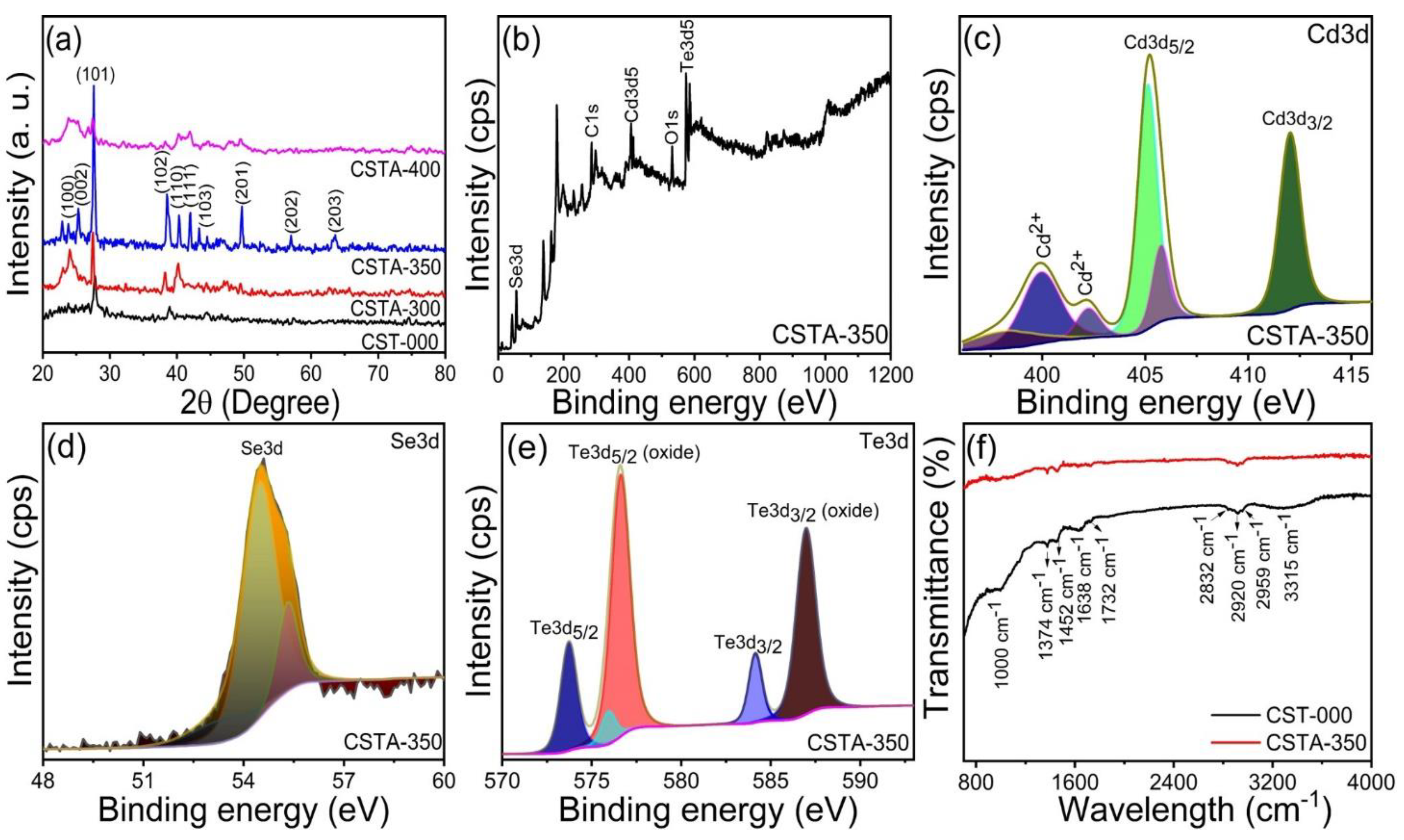
2.1. X-ray Diffraction
2.2. X-ray Photoelectron Spectroscopy
2.3. FT-IR
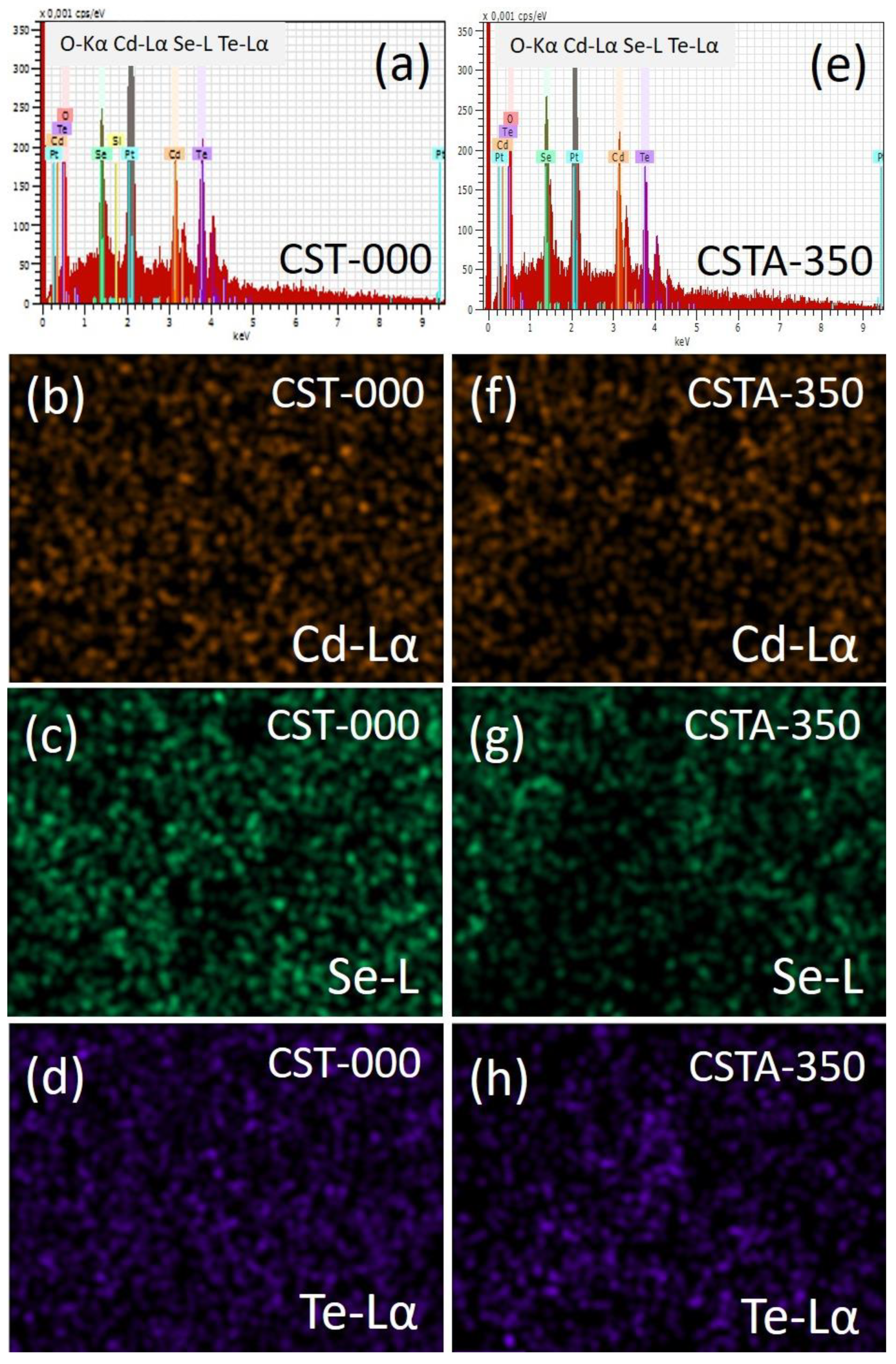
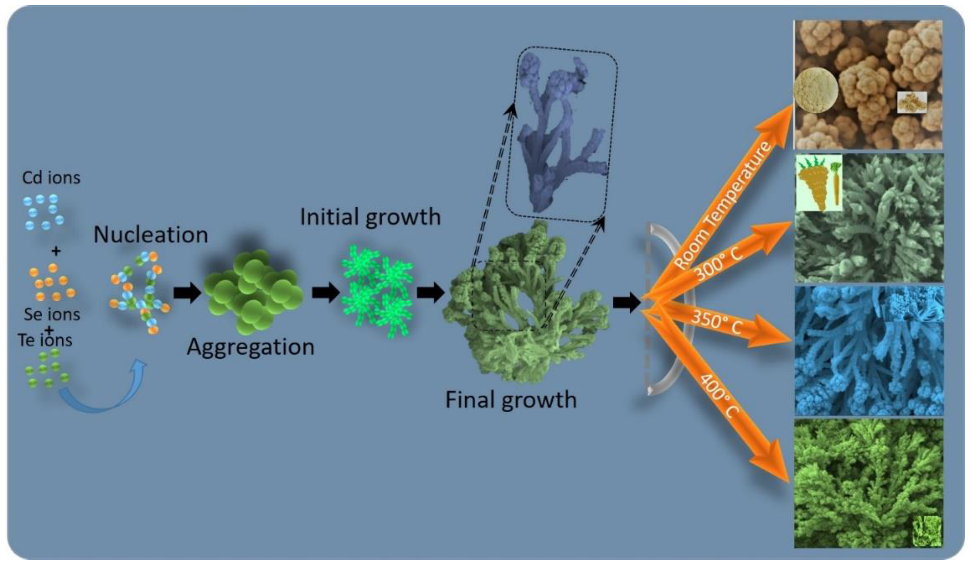
2.4. FE-SEM
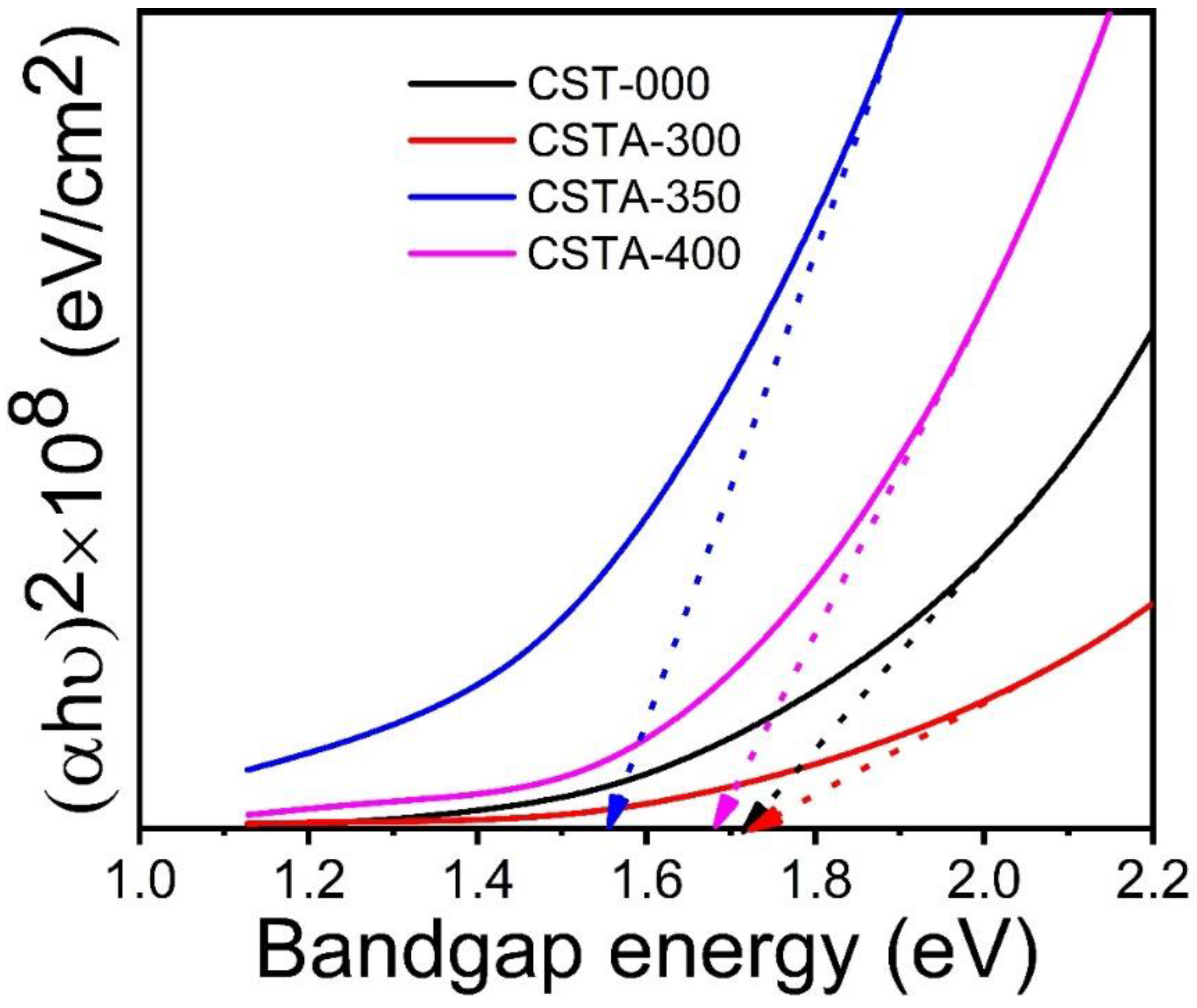
2.5. Band Gap Energy Study
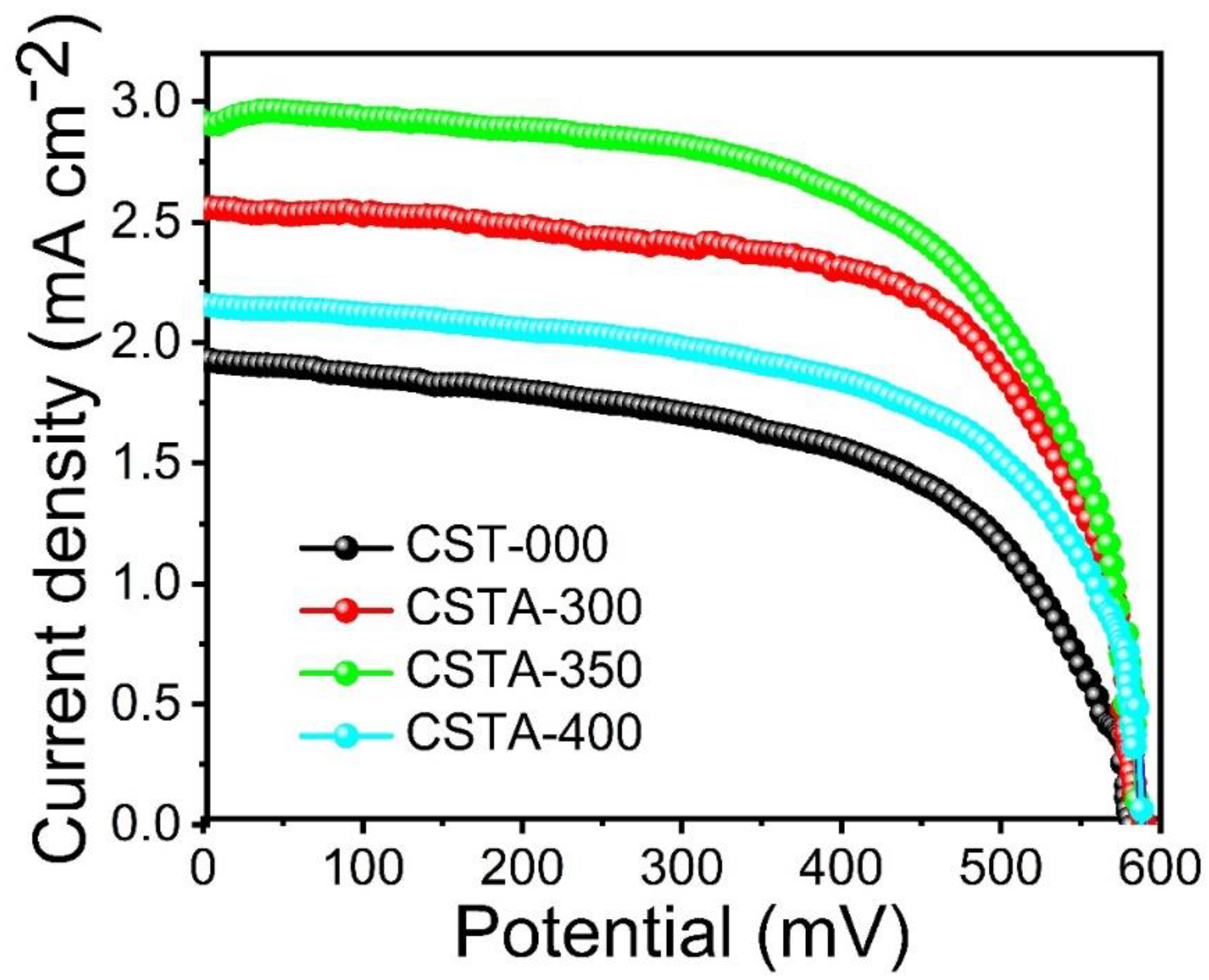
2.6. Photoelectrochemical Study
3. Materials and Methods
3.1. Materials
3.2. Synthesis of CdTe0.6Se0.4 Thin Films
3.3. Characterization Techniques
3.4. Electrode Preparation and PEC Measurements
4. Conclusions
Supplementary Materials
Author Contributions
Funding
Data Availability Statement
Acknowledgments
Conflicts of Interest
References
- Chang, H.; Wu, H. Graphene-based nanocomposites: Preparation, functionalization, and energy and environmental applications. Energy Environ. Sci. 2013, 6, 3483–3507. [Google Scholar] [CrossRef]
- Sun, M.-H.; Huang, S.-Z.; Chen, L.-H.; Li, Y.; Yang, X.-Y.; Yuan, Z.-Y.; Su, B.-L. Applications of hierarchically structured porous materials from energy storage and conversion, catalysis, photocatalysis, adsorption, separation, and sensing to biomedicine. Chem. Soc. Rev. 2016, 45, 3479–3563. [Google Scholar] [CrossRef]
- Antoniadou, M.; Kondarides, D.I.; Dionysiou, D.D.; Lianos, P. Quantum dot sensitized titania applicable as photoanode in photoactivated fuel cells. J. Phys. Chem. C 2012, 116, 16901–16909. [Google Scholar] [CrossRef]
- De, B.; Karak, N. Recent progress in carbon dot–metal based nanohybrids for photochemical and electrochemical applications. J. Mater. Chem. A 2017, 5, 1826–1859. [Google Scholar] [CrossRef]
- Yang, J.; Wang, J.; Zhao, K.; Izuishi, T.; Li, Y.; Shen, Q.; Zhong, X. CdSeTe/CdS Type-I Core/Shell Quantum Dot Sensitized Solar Cells with Efficiency over 9%. J. Phys. Chem. C 2015, 119, 28800–28808. [Google Scholar] [CrossRef]
- Su, X.; Chen, Y.; Ren, L.; He, Y.; Yin, X.; Liu, Y.; Yang, W. Cobalt catalyst grafted CdSeTe quantum dots on porous NiO as photocathode for H2 evolution under visible light. ACS Sustain. Chem. Eng. 2019, 7, 11166–11174. [Google Scholar] [CrossRef]
- Zhang, Y.; Yin, P.F.; Liu, X.; Mao, J.; Kulinich, S.A.; Du, X. Tuning band structure of cadmium chalcogenide nanoflake arrays via alloying for efficient photoelectrochemical hydrogen evolution. Langmuir 2017, 33, 6457–6463. [Google Scholar] [CrossRef]
- Zou, H.; Liu, M.; Zhou, D.; Zhang, X.; Liu, Y.; Yang, B.; Zhang, H. Employing CdSexTe1–x alloyed quantum dots to avoid the temperature-dependent emission shift of light-emitting diodes. J. Phys. Chem. C 2017, 121, 5313–5323. [Google Scholar] [CrossRef]
- Hu, C.; Li, M.; Qiu, J.; Sun, Y.P. Design and fabrication of carbon dots for energy conversion and storage. Chem. Soc. Rev. 2019, 48, 2315–2337. [Google Scholar] [CrossRef]
- Das, A.K.; Paria, S.; Maitra, A.; Halder, L.; Bera, A.; Bera, R.; Si, S.K.; De, A.; Ojha, S.; Bera, S.S.K.; et al. Highly rate capable nanoflower-like NiSe and WO3@PPy composite electrode materials toward high energy density flexible all-solid-state asymmetric supercapacitor. ACS Appl. Electron. Mater. 2019, 1, 977–990. [Google Scholar] [CrossRef]
- Das, A.; Deepa, M.; Ghosal, P. Dual function of molybdenum sulfide/C-cloth in enhancing the performance of fullerene nanosheets based solar cell and supercapacitor. RSC Adv. 2018, 8, 34984–34998. [Google Scholar] [CrossRef] [Green Version]
- Zhu, S.; Li, Q.; Wei, Q.; Sun, R.; Liu, X.; An, Q.; Mai, L. NiSe2 Nanooctahedra as an anode material for high-rate and long-life sodium-ion battery. ACS Appl. Mater. Interfaces 2017, 9, 311–316. [Google Scholar] [CrossRef]
- Kumar, P.N.; Narayanan, R.; Deepa, M.; Srivastava, A.K. Au@poly(acrylic acid) plasmons and C60 improve the light harvesting capability of a TiO2/CdS/CdSeS photoanode. J. Mater. Chem. A 2014, 2, 9771–9783. [Google Scholar] [CrossRef]
- Pareek, A.; Paik, P.; Borse, P.H. Nanoniobia modification of CdS photoanode for an efficient and stable photoelectrochemical cell. Langmuir 2014, 30, 15540–15549. [Google Scholar] [CrossRef]
- Vercelli, B.; Zotti, G.; Berlin, A. Alternate monolayers of CdSe nanocrystals and perylene tetracarboxylate: Quantum dot hypersensitization for dye-sensitized solar cells. ACS Appl. Mater. Interfaces 2012, 4, 3233–3238. [Google Scholar] [CrossRef]
- Zhang, J.; Su, Y.; Zhu, Y.; Yun, J.; Yang, X. Photoelectrochemical biofuel cell with dendrimer-encapsulated CdSe nanoparticles-sensitized titanium dioxide as the photoanode. New J. Chem. 2014, 38, 2300–2304. [Google Scholar] [CrossRef]
- Wang, J.; Lv, P.; Mu, Y.; Ding, D.; Liu, L.; Runa, A.; Feng, F.; Feng, S.; Fu, W.; Yang, H. A novel cage-like CdTe film with enhanced photoelectrochemical performance. RSC Adv. 2016, 6, 43489–43495. [Google Scholar] [CrossRef]
- Kurnia, F.; Ng, Y.H.; Tang, Y.; Amal, R.; Valanoor, N.; Hart, J.N. ZnS thin films for visible-light active photoelectrodes: Effect of film morphology and crystal structure. Cryst. Growth Des. 2016, 5, 2461–2465. [Google Scholar] [CrossRef]
- Kowalik, R.; Szaciłowski, K.; Żabiński, P. Photoelectrochemical study of ZnSe electrodeposition on Cu electrode. J. Electroanal. Chem. 2012, 674, 108–112. [Google Scholar] [CrossRef]
- Jia, J.; Xue, P.; Hu, X.; Wang, Y.; Liu, E.; Fan, J. Electron-transfer cascade from CdSe@ZnSe core-shell quantum dot accelerates photoelectrochemical H2 evolution on TiO2 nanotube arrays. J. Catal. 2019, 375, 81–94. [Google Scholar] [CrossRef]
- Bhagyaraj, S.; Perumbilavil, S.; Udayabashkar, R.; Mangalaraja, R.V.; Thomas, S.; Kalarikkal, N.; Oluwafemi, O.S.; Sreekanth, P.; Rednam, U.; Viswanathan, M.R. Tuning of nonlinear absorption in highly luminescent CdSe based quantum dots with core–shell and core/multi-shell architectures. Phys. Chem. Chem. Phys. 2019, 21, 11424–11434. [Google Scholar] [CrossRef] [PubMed]
- Rosly, H.N.; Rahman, K.S.; Abdullah, S.F.; Harif, M.N.; Doroody, C.; Chelvanathan, P.; Misran, H.; Sopian, K.; Amin, N. The Role of Deposition Temperature in the Photovoltaic Properties of RF-Sputtered CdSe Thin Films. Crystals 2021, 11, 73. [Google Scholar] [CrossRef]
- Amir, F.; Clark, K.; Maldonado, E.; Kirk, W.; Jiang, J.; Ager, J.; Yu, K.; Walukiewicz, W. Epitaxial growth of CdSexTe1−x thin films on Si(100) by molecular beam epitaxy using lattice mismatch graded structures. J. Cryst. Growth 2008, 310, 1081–1087. [Google Scholar] [CrossRef]
- Matsumura, N.; Sakamoto, T.; Saraie, J. Growth conditions in molecular beam epitaxy for controlling CdSeTe epilayer composition. J. Cryst. Growth 2003, 251, 602–606. [Google Scholar] [CrossRef]
- Noda, D.; Aoki, T.; Nakanishi, Y.; Hatanak, Y. Growth of CdZnTe and CdSeTe crystals for p–i–n radiation detectors. J. Cryst. Growth 2000, 2, 1121–1124. [Google Scholar] [CrossRef]
- Wei, W.; Yang, Z.; Song, W.; Hu, F.; Luan, B.; Li, P.; Yin, H. Different CdSeTe structure determined photoelectrocatalytic reduction performance for carbon dioxide. J. Colloid Interf. Sci. 2017, 496, 327–333. [Google Scholar] [CrossRef] [PubMed]
- Munshi, A.H.; Kephart, J.M.; Abbas, A.; Danielson, A.; Gḗlinas, G.; Beaudry, J.-N.; Barth, K.L.; Walls, J.M.; Sampath, W.S. Effect of CdCl2 passivation treatment on microstructure and performance of CdSeTe/CdTe thin-film photovoltaic devices. Sol. Energy Mater. Sol. C 2018, 186, 256–259. [Google Scholar] [CrossRef] [Green Version]
- Murali, K.R. Characteristics of slurry coated CdSeTe films. Mater. Sci. Semicon. Proc. 2010, 13, 193–198. [Google Scholar] [CrossRef]
- Liu, G.; Ling, Z.; Wang, Y.; Zhao, H. Near-infrared CdSexTe1−X@CdS “giant” quantum dots for efficient photoelectrochemical hydrogen generation. Int. J. Hydrog. Energy 2018, 43, 22064–22074. [Google Scholar] [CrossRef]
- Hana, Z.; Chen, L.; Weng, Q.; Zhou, Y.; Wang, L.; Li, C.; Chen, J. Silica-coated gold nanorod@CdSeTe ternary quantum dots core/shell structure for fluorescence detection and dual-modal imaging. Sens. Actuators B 2018, 258, 508–516. [Google Scholar] [CrossRef]
- Shinde, S.K.; Thombare, J.V.; Dubal, D.P.; Fulari, V.J. Electrochemical synthesis of photosensitive nano-nest like CdSe0.6Te0.4 thin films. Appl. Surf. Sci. 2013, 282, 561–565. [Google Scholar] [CrossRef]
- Shinde, S.; Dubal, D.; Ghodake, G.; Fulari, V. Synthesis and characterization of chemically deposited flower-like CdSe0.6Te0.4 thin films for solar cell application. Mater. Lett. 2014, 126, 17–19. [Google Scholar] [CrossRef]
- Shinde, S.K.; Ghodake, G.S.; Maile, N.C.; Dhaygude, H.D.; Kim, S.; Phule, A.D.; Patel, R.V.; Kim, D.Y. Porous CdSe0.6Te0.4 nanoflowers-nanosphere: Facile electrochemical synthesis and excellent for photoelectrochemical cell performance. Ionics 2017, 23, 2489–2496. [Google Scholar] [CrossRef]
- Shinde, S.K.; Ghodake, G.S.; Dubal, D.P.; Dhaygude, H.D.; Kim, D.-Y.; Rath, M.C.; Fulari, V.J. Morphological modification of CdSe0.6Te0.4 nanostructures by electron irradiation and the effect on photoelectrochemical cells. J. Mater. Sci.-Mater. Electron. 2017, 28, 1976–1984. [Google Scholar] [CrossRef]
- Shinde, S.K.; Ghodake, G.S.; Dubal, D.P.; Lohar, G.M.; Lee, D.S.; Fulari, V.J. Structural, optical, and photo-electrochemical properties of marygold-like CdSe0.6Te0.4 synthesized by electrochemical route. Ceram. Int. 2014, 40, 11519–11524. [Google Scholar] [CrossRef]
- Shinde, S.K.; Dubal, D.P.; Ghodake, G.S.; Fulari, V.J. Electronic impurities (Fe, Mn) doping in CdSe nanostructures for improvements in photoelectrochemical applications. RSC Adv. 2014, 4, 33184–33189. [Google Scholar] [CrossRef] [Green Version]
- Shinde, S.K.; Dubal, D.P.; Ghodake, G.S.; Lee, D.S.; Lohar, G.M.; Rath, M.C.; Fulari, V.J. Materials Baking impact of Fe composition on CdSe films for solar cell application. Mater. Lett. 2014, 132, 243–246. [Google Scholar] [CrossRef]
- Ghodake, V.J.; Fulari, D.-Y.; Kim, D.Y. High electrochemical performance of nanoflakes like CuO electrode by successive ionic layer adsorption and reaction (SILAR) method. J. Ind. Eng. Chem. 2017, 52, 12–17. [Google Scholar]
- Shinde, S.; Jalak, M.; Ghodake, G.; Maile, N.; Yadav, H.; Jagadale, A.; Shahzad, A.; Lee, D.; Kadam, A.; Fulari, V.; et al. Flower-like NiCo2O4/NiCo2S4 electrodes on Ni mesh for higher supercapacitor applications. Ceram. Int. 2019, 45, 17192–17203. [Google Scholar] [CrossRef]
- Dhaygude, H.D.; Shinde, S.K.; Takale, M.V.; Dubal, D.P.; Lohar, G.M.; Fulari, V.J. Electrodeposited nanosphere like CdxZn12xS electrodes for photoelectrochemical cell. J. Mater. Sci. Mater. Electron. 2016, 27, 5145–5152. [Google Scholar] [CrossRef]
- MacDonald, B.I.; Martucci, A.; Rubanov, S.; Watkins, S.E.; Mulvaney, P.; Jasieniak, J.J. Layer-by-layer assembly of sintered CdSexTe1−X nanocrystal solar Cells. ACS Nano 2012, 6, 5995–6004. [Google Scholar] [CrossRef]
- Marcos, L.V.R. –D.; Kalaiselvi, S.M.P.; Leong, O.B.; Das, P.K.; Breese, M.B.H.; Rusydio, A. Optical constants and absorption properties of Te and TeO thin films in the 13-14 nm spectral range. Opt. Express 2020, 28, 12922–12935. [Google Scholar] [CrossRef] [PubMed]
- Shinde, S.K.; Ghodake, G.S.; Dubal, D.P.; Dhaygude, H.D.; Kim, D.-Y.; Fulari, V.J. Enhanced photoelectrochemical properties of nanoflower-like hexagonal CdSe0.6Te0.4: Effect of electron beam irradiation. J. Ind. Eng. Chem. 2017, 45, 92–98. [Google Scholar] [CrossRef]
- Xue, J.; Chen, X.; Liu, S.; Zheng, F.; He, L.; Li, L.; Zhu, J.-J. Highly Enhanced Fluorescence of CdSeTe Quantum Dots Coated with Polyanilines via In-Situ Polymerization and Cell Imaging Application. ACS Appl. Mater. Interfaces 2015, 7, 19126–19133. [Google Scholar] [CrossRef]
- Li, Z.-J.; Fan, X.-B.; Li, X.-B.; Li, J.-X.; Zhan, F.; Tao, Y.; Zhang, X.; Kong, Q.-Y.; Zhao, N.-J.; Zhang, J.-P.; et al. Direct synthesis of all-inorganic heterostructured CdSe/CdS QDs in aqueous solution for improved photocatalytic hydrogen generation. J. Mater. Chem. A 2017, 5, 10365–10373. [Google Scholar] [CrossRef]
- Yuan, Y.-J.; Chen, D.; Yu, Z.-T.; Zou, Z.-G. Cadmium sulfide-based nanomaterials for photocatalytic hydrogen production. J. Mater. Chem. A 2018, 6, 11606–11630. [Google Scholar] [CrossRef]
- Dhaygude, H.; Shinde, S.; Takale, M.; Lohar, G.; Rath, M.; Fulari, V. Effect of electron irradiation on structural, morphological and photoluminescence properties of ZnS thin films. Ceram. Int. 2016, 42, 10159–10164. [Google Scholar] [CrossRef]
- Dhaygude, H.D.; Shinde, S.K.; Dubal, D.P.; Rath, M.C.; Fulari, V.J. Effect of electron beam irradiation on electro synthesized hexagonal Cd0.3Zn0.7S nanosphere with excellent application in solar cell. Appl. Surf. Sci. 2016, 368, 1–7. [Google Scholar] [CrossRef]
- Shinde, S.K.; Ghodake, G.S.; Velhal, N.B.; Takale, M.V.; Kim, D.-Y.; Rath, M.C.; Dhaygude, H.D.; Fulari, V.J. Enhanced solar cell performance of electron beam irradiated CdS photoanode by electrodeposition method. J. Solid State Electr. 2017, 21, 1517–1522. [Google Scholar] [CrossRef]
- Shinde, S.K.; Kim, D.-Y.; Lee, D.S.; Ghodake, G.S.; Kadam, A.N.; Fulari, A.V.; Nawaz, M.; Shahzad, A.; Rath, M.C.; Fulari, V.J. Effect of electron beam irradiation on chemically synthesized nanoflake-like CdS electrodes for photoelectrochemical applications. Colloids Surf. B 2018, 164, 255–261. [Google Scholar] [CrossRef] [PubMed]
- Pan, A.; Yang, H.; Liu, R.; Yu, R.; Zou, B.; Wang, Z. Color-tunable photoluminescence of alloyed CdSxSe1−X nanobelts. J. Am. Chem. Soc. 2005, 127, 15692–15693. [Google Scholar] [CrossRef]
- Pan, J.; Utama, M.I.B.; Zhang, Q.; Liu, X.; Peng, B.; Wong, L.M.; Sum, T.C.; Wang, S.; Xion, Q. Composition-tunable vertically aligned CdSxSe1−X nanowire arrays via van der waals epitaxy: Investigation of optical properties and photocatalytic behavior. Adv. Mater. 2012, 24, 4151–4156. [Google Scholar] [CrossRef]
- Muthukumarasamy, N.; Balasundaraprabhu, R.; Jayakumar, S.; Kannan, M.D.; Ramanathaswamy, P. Compositional dependence of optical properties of hot wall deposited CdSexTe1−X thin films. Phys. Stat. Sol. 2004, 201, 2312–2318. [Google Scholar] [CrossRef]
- Velumani, S.; Mathew, X.; Sebastian, P.J. Structural and optical characterization of hot wall deposited CdSexTe1−x films. Sol. Energ. Mater. Sol. C 2003, 76, 359–368. [Google Scholar] [CrossRef]
- Sathyamoorthy, R.; Sudhagar, P.; Kumar, R.S.; Matheswaran, P.; Nair, R.G. Facile synthesis of thiol-stabilized CdSexTe1−x nanocrystals. Phys. B 2011, 406, 715–719. [Google Scholar] [CrossRef]


| Samples Names/ID | Imax (mA/cm2) | Vmax (mV/cm2) | VOC (mV/cm2) | ISC (mA/cm2) | Fill Factor | Efficiency (η) % |
|---|---|---|---|---|---|---|
| CST-000 | 1.50 | 409.21 | 658.37 | 1.91 | 0.49 | 2.0 |
| CSTA-300 | 2.30 | 407.71 | 671.04 | 2.59 | 0.54 | 3.1 |
| CSTA-350 | 2.66 | 407.14 | 680.25 | 2.96 | 0.53 | 3.6 |
| CSTA-400 | 1.83 | 413.13 | 697.29 | 2.19 | 0.50 | 2.5 |
Publisher’s Note: MDPI stays neutral with regard to jurisdictional claims in published maps and institutional affiliations. |
© 2021 by the authors. Licensee MDPI, Basel, Switzerland. This article is an open access article distributed under the terms and conditions of the Creative Commons Attribution (CC BY) license (https://creativecommons.org/licenses/by/4.0/).
Share and Cite
Ghodake, G.S.; Kim, D.-Y.; Shinde, S.K.; Dubal, D.P.; Yadav, H.M.; Magotra, V.K. Impact of Annealing Temperature on the Morphological, Optical and Photoelectrochemical Properties of Cauliflower-like CdSe0.6Te0.4 Photoelectrodes; Enhanced Solar Cell Performance. Int. J. Mol. Sci. 2021, 22, 11610. https://doi.org/10.3390/ijms222111610
Ghodake GS, Kim D-Y, Shinde SK, Dubal DP, Yadav HM, Magotra VK. Impact of Annealing Temperature on the Morphological, Optical and Photoelectrochemical Properties of Cauliflower-like CdSe0.6Te0.4 Photoelectrodes; Enhanced Solar Cell Performance. International Journal of Molecular Sciences. 2021; 22(21):11610. https://doi.org/10.3390/ijms222111610
Chicago/Turabian StyleGhodake, Gajanan S., Dae-Young Kim, Surendra K. Shinde, Deepak P. Dubal, Hemraj M. Yadav, and Verjesh Kumar Magotra. 2021. "Impact of Annealing Temperature on the Morphological, Optical and Photoelectrochemical Properties of Cauliflower-like CdSe0.6Te0.4 Photoelectrodes; Enhanced Solar Cell Performance" International Journal of Molecular Sciences 22, no. 21: 11610. https://doi.org/10.3390/ijms222111610