Article

Tunable Contact Types and Interfacial Electronic Properties in TaS2/MoS2 and TaS2/WSe2 Heterostructures

Key Laboratory of Functional Materials Physics and Chemistry of the Ministry of Education, Key Laboratory of Preparation and Application of Environmental Friendly Materials, College of Physics, Jilin Normal University, Changchun 130103, China
*
Authors to whom correspondence should be addressed.
Molecules 2023, 28(14), 5607; https://doi.org/10.3390/molecules28145607
Submission received: 8 June 2023 / Revised: 18 July 2023 / Accepted: 19 July 2023 / Published: 24 July 2023
(This article belongs to the Topic Advances in Computational Materials Sciences)

Abstract

:
Following the successful experimental synthesis of single-layer metallic 1T-TaS2 and semiconducting 2H-MoS2, 2H-WSe2, we perform a first-principles study to investigate the electronic and interfacial features of metal/semiconductor 1T-TaS2/2H-MoS2 and 1T-TaS2/2H-WSe2 van der Waals heterostructures (vdWHs) contact. We show that 1T-TaS2/2H-MoS2 and 1T-TaS2/2H-WSe2 form n-type Schottky contact (n-ShC type) and p-type Schottky contact (p-ShC type) with ultralow Schottky barrier height (SBH), respectively. This indicates that 1T-TaS2 can be considered as an effective metal contact with high charge injection efficiency for 2H-MoS2, 2H-WSe2 semiconductors. In addition, the electronic structure and interfacial properties of 1T-TaS2/2H-MoS2 and 1T-TaS2/2H-WSe2 van der Waals heterostructures can be transformed from n-type to p-type Schottky contact through the effect of layer spacing and the electric field. At the same time, the transition from Schottky contact to Ohmic contact can also occur by relying on the electric field and different interlayer spacing. Our results may provide a new approach for photoelectric application design based on metal/semiconductor 1T-TaS2/2H-MoS2 and 1T-TaS2/2H-WSe2 van der Waals heterostructures.

1. Introduction

Due to their remarkable material properties and enormous potential for use in a wide variety of technological device applications, novel 2D materials have attracted a significant amount of attention from researchers. Graphene [1,2] as the first material to promote the field of 2D materials research has many remarkable properties, such as massless Dirac fermions [3], high carrier mobility [4], high conductivity [5], and an unconventional quantum Hall effect at room temperature [6]. However, high-speed electrical applications like field-effect transistors are limited by the lack of a bandgap in graphene [7]. Therefore, the research community has been actively searching for 2D semiconductor materials with excellent properties and applications. In recent years, TMDs, a whole new class of 2D materials, have been studied as the most attractive materials due to their excellent properties. Because of their inherent advantages, such as a high surface-to-volume ratio, no dangling bonds, and excellent carrier mobility, TMDs [8,9,10,11] are important technical materials for various energy, electronic, and optoelectronic applications in the future.
Among TMDs, 2H-MoS2 and 2H-WSe2, the two most typical TMDs materials, have fascinating properties and a wide range of applications. The bulk structure of MoS2 is stratified, with weak van der Waals (vdW) forces between layers. Unlike graphene, monolayer MoS2 is a direct bandgap [7,8] semiconductor with a bandgap of 1.8 eV. Moreover, single-layer MoS2 has a high on/off current ratio of about 108 and a high carrier mobility [9] of 200 cm2/V−1s−1 at room temperature, making it promising in field-effect transistors [7] (FETs), photodetectors [10], and electroluminescent devices, thus demonstrating its considerable application potential. So far, the structural, mechanical, electronic, and transport properties of MoS2 monolayers have been extensively studied, both experimentally and theoretically [11,12,13,14,15,16,17]. The results show that the physical properties of MoS2 monomolecular film are very sensitive to external conditions, such as the strain and electric field. Furthermore, 2D WSe2 is an indirect bandgap semiconductor with a rather large bandgap. In the past few years, the electronic properties, thermoelectric response [18], and strain engineering [11,19,20,21] of WSe2 have been extensively studied. At the same time, important applications of WSe2 in transistors [22,23,24], phototransistors [25], circuits [26,27], and magnesium-ion batteries [28] have also been discussed. Furthermore, single-layer and few-layer WSe2 have been experimentally synthesized [29,30,31], which makes the fabrication of high-performance WSe2-based nanoelectronics devices promising. Different from 2D MoS2 and WSe2 monolayers, we note that 1T-TaS2, as an emerging 2D layered TMD, is one of the most studied TMDs due to its unexpected physical properties. The structure of 1T-TaS2 is similar to the 2H phase of MoS2, but it exhibits different metallic properties [32,33], so it is very important for our next research work.
The electrical contacts between metals and semiconductors are frequently used in modern electronic and optoelectronic devices, which can not only greatly improve the charge injection efficiency of semiconductors, but also improve the performance of electronic devices. The study of metal/semiconductor interfacial contacts is a crucial step in the construction of energy-efficient and high-performance electronic devices. The functionality of the device may be compromised partially or totally in the event of inappropriate contact between the metal and the semiconductor. Therefore, the formation of a low or eliminated Schottky barrier height (SBH) [22,34] in the metal-semiconductor junction (MSJ) from the Schottky to the ohmic contact is critical for the fabrication of high-performance nanodevices. Since most 2D metal-semiconductor interfaces are essentially Schottky interfaces [35,36], there will be intrinsic and extrinsic limitations, including surface defects, work function mismatch, and sustainable doping strategies; thus, Schottky Converting base contact to ohmic contact is indeed a challenging task.
The high contact resistance [37] of transition metal dichalcogenide (TMDs) devices is one of the bottlenecks limiting the application of TMDs in various fields. The contact [38] resistance of TMD-based devices is closely related to the contacted metal/TMDs interface and band alignment [39]. So far, a large number of theoretical experiments [40] have demonstrated that the vdW interaction can generate good contact properties in metal-transition metals [41,42] and semimetals-transition metals [43]. Therefore, vdW contacts have a very wide range of applications.
To date, the tunable Schottky barrier and electronic properties of the 1T-TaS2/2H-MoS2 (2H-WSe2) combination have not yet been investigated. Based on this idea, we constructed 1T-TaS2, 2H-MoS2 (2H-WSe2) monolayer structures, respectively. In this work, we performed first-principles calculations to investigate the atomic and electronic structures of 1T-TaS2/2H-MoS2 (2H-WSe2) vdWHs and their tunable electronic structures under interlayer spacing and the electric field. The vdW interaction between metallic 1T-TaS2 and semiconducting 2H-MoS2 (2H-WSe2) monolayers makes the heterostructure energetically feasible and preserves the intrinsic properties of the two constituent monolayers. Our results predict that 1T-TaS2/2H-MoS2 (2H-WSe2) vdWHs have a tunable Schottky barrier height (SBH), and that the electronic structure and interfacial properties of 1T-TaS2/2H-MoS2 (2H-WSe2) vdWHs can be transformed from n-type to p-type ShC through the effect of layer spacing and the electric field. At the same time, the transition from ShC to OhC can also occur by relying on the electric field and different interlayer spacing. Our results reveal the potential role of metallic 1T-TaS2 as an effective metal contact to semiconductor 2H-MoS2 (2H-WSe2).

2. Results and Discussion

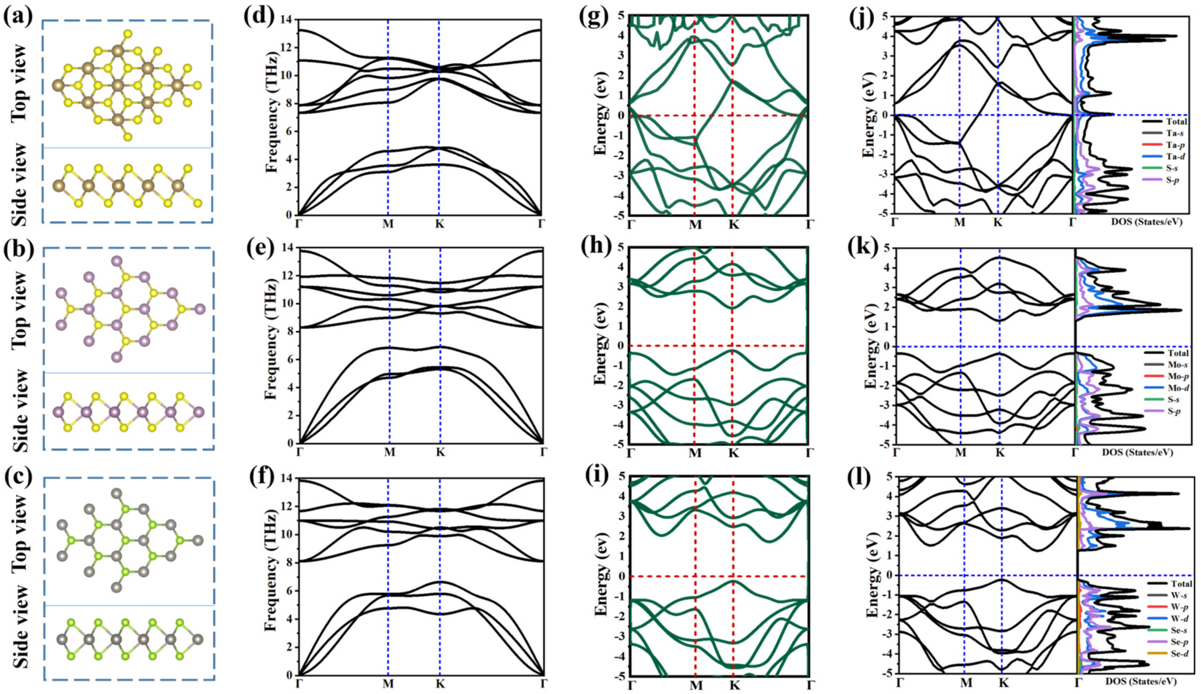
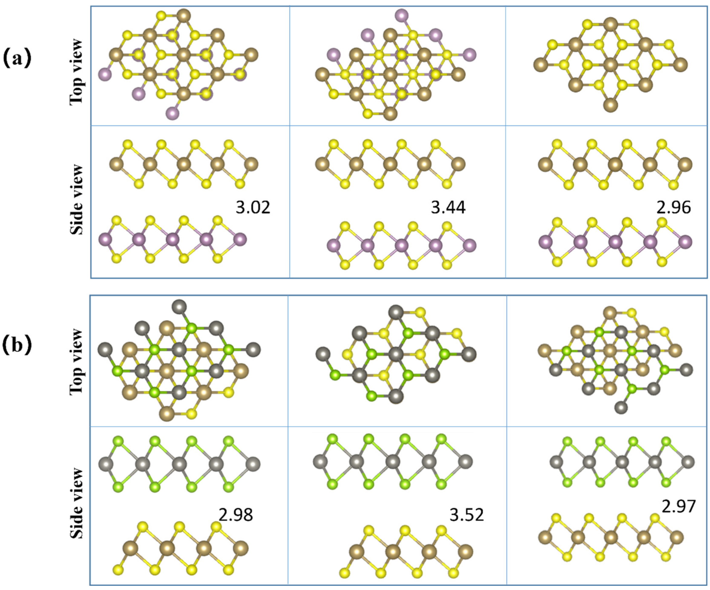
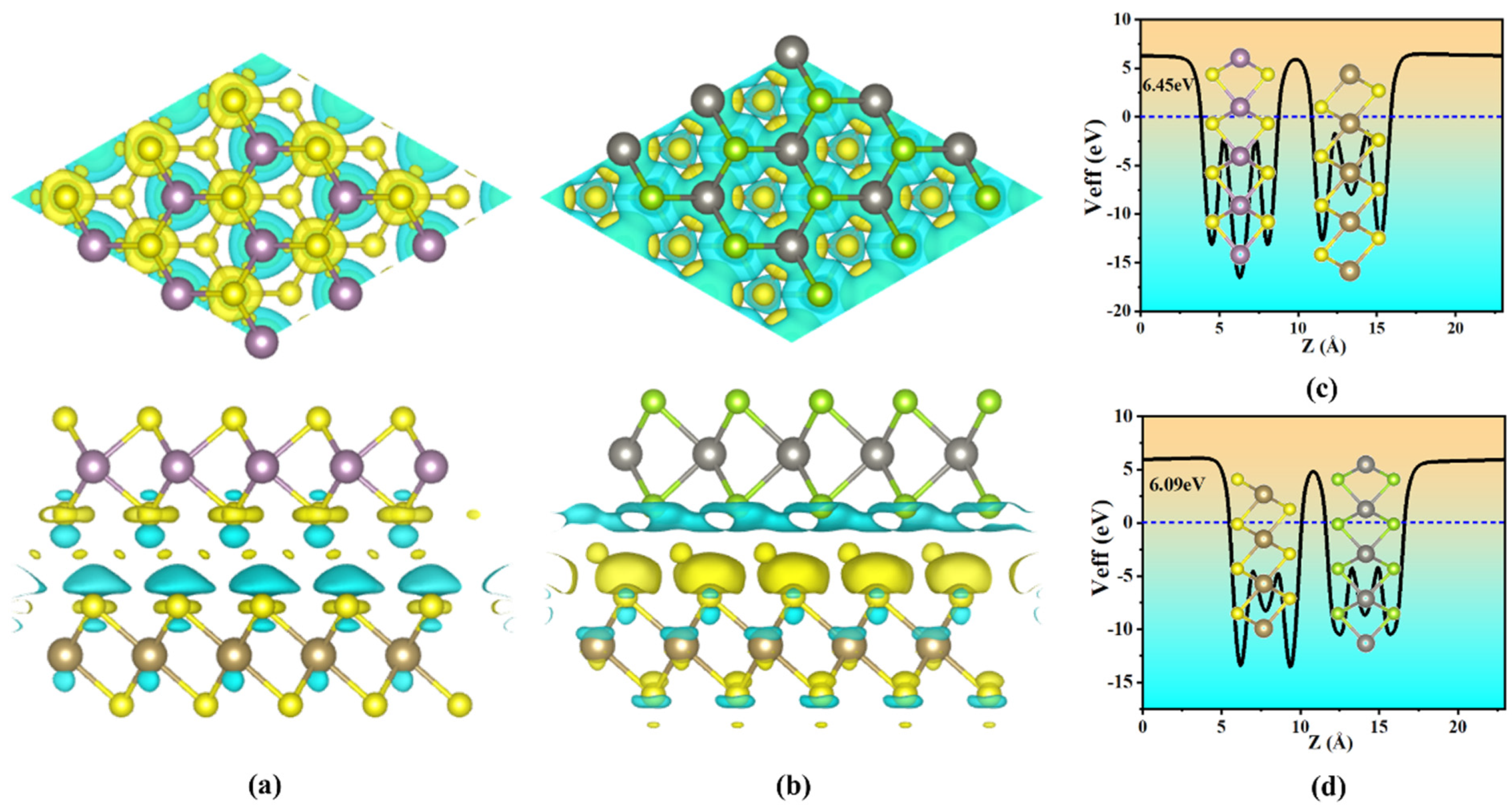
2.1. Geometric Structures and Electronic Properties

In Figure 1, we showed the atomic structure, phonon spectrum, projected band structure, and state density of metallic 1T-TaS2 and semiconducting 2H-MoS2, 2H-WSe2 monolayer. After geometric optimization, the monolayers 1T-TaS2, 2H-MoS2, and 2H-WSe2 all show layered atomic structures, and their lattice constants are 3.186 Å, 3.184 Å, and 3.184 Å, respectively, which is consistent with previous experimental and theoretical measurements. In Figure 1a–c, it can be seen that the Ta atom in metal TaS2 is sandwiched between two S atoms, while the Mo atom and W atom are sandwiched between two S atoms and two Se atoms in semiconductor MoS2 and WSe2 monolayers, respectively. In addition, the 1T-TaS2 layer in Figure 1g shows metallic behavior, while the 2H-MoS2 and 2H-WSe2 monolayers in Figure 1h, ishow semiconductor characteristics. 2H-MoS2 shows a direct bandgap semiconductor while 2H-WSe2 shows an indirect bandgap semiconductor. The bandgap values calculated by HSE06 are 2.32 eV and 1.97 eV, and those calculated by PBE are 1.66 eV and 1.46 eV, respectively. The results show that they are close to the experimental measurements [11] of 1.80 eV and 1.65 eV, which confirms the reliability of our calculation. In general, traditional PBE methods often underestimate the bandgap of 2D semiconductors, and HSE06 can be used to predict more accurate bandgap values. However, the PBE bandgap of the 2H-MoS2 and 2H-WSe2 monolayers is closer to the experimental bandgap than the HSE06 method. Therefore, we use the PBE method for all of the following calculations. Moreover, in Figure 1h,i, it is found that, in both PBE and HSE06 functional, the CBM and VBM of 2H-MoS2 monolayer are located at the K point, while the CBM and VBM of 2H-WSe2 monolayer are not at the same high-symmetry path. In addition, the state density of 1T-TaS2 is shown in Figure 1g. For metal 1T-TaS2, the major contribution is the d orbital of Ta. Meanwhile, for the 2H-MoS2 monolayer, the CBM is dominated by the d orbital contribution of Mo, and the VBM is dominated by the p orbital contribution of S. For the 2H-WSe2 monolayer, the CBM is dominated by the d orbital contribution of W, and the VBM is dominated by the p orbital contribution of Se. The phonon spectrum of 1T-TaS2,2H-MoS2 and 2H-WSe2 are reflected in Figure 1d–f. It can be seen that the frequencies of the three considered monolayers are all positive, and there is no negative frequency at the Γ point, thus confirming their dynamic stability.

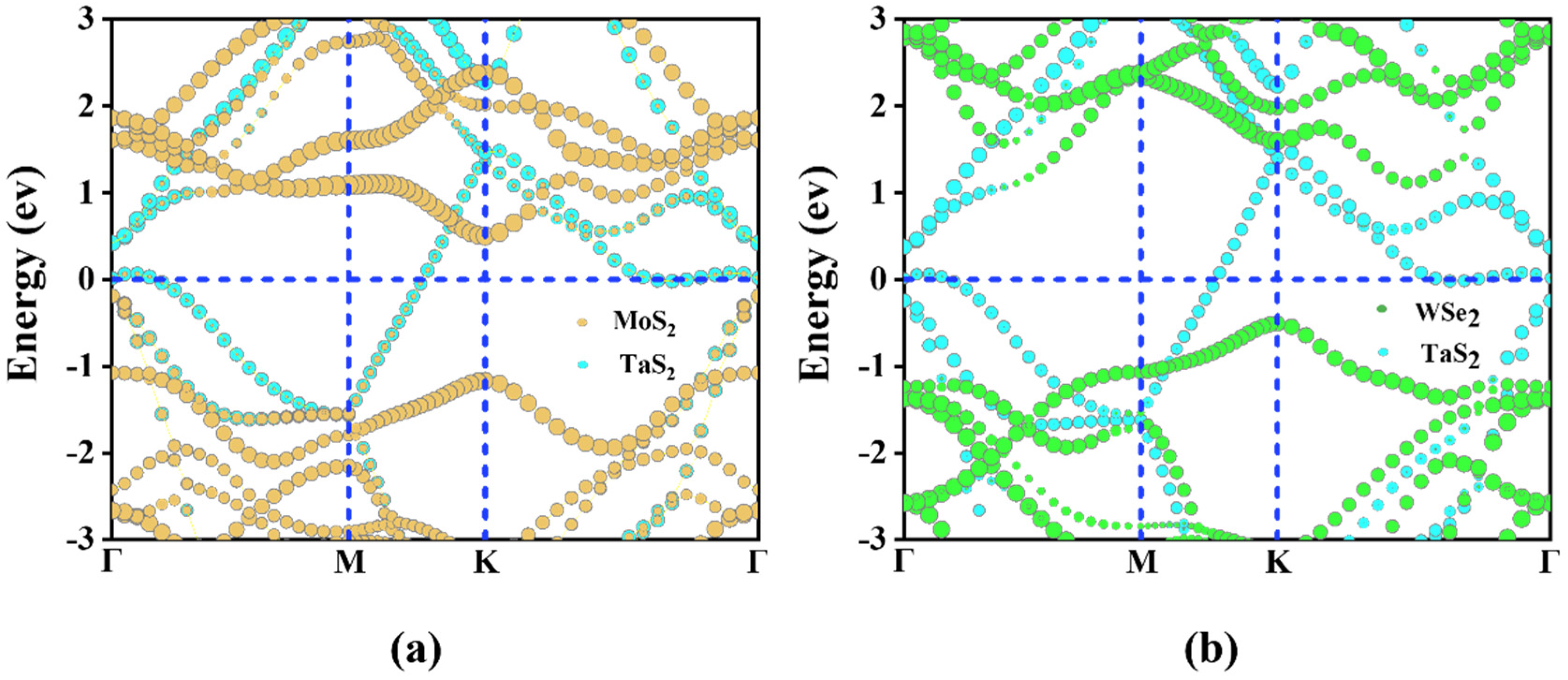
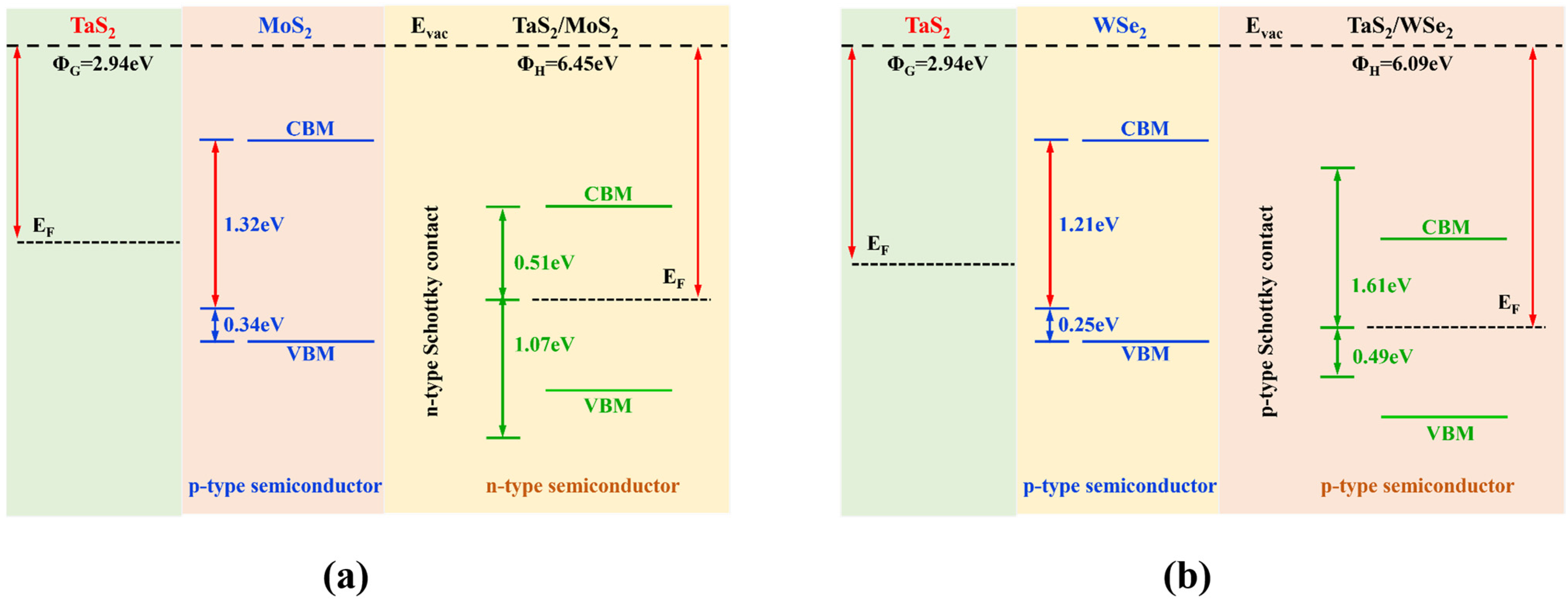
2.2. Structures and Electronic Properties of Heterostructures

We constructed vdWHs by stacking the monolayers 2H-MoS2 and 2H-WSe2 in the 1T-TaS2 monolayer along the z direction and setting the initial equilibrium layer spacing D as 3.02 Å and 2.98 Å, which are greater than the sum of the covalent radii between Mo and S atoms and W and Se atoms, respectively. This confirmed that no covalent bond has been formed between the two constituent monolayers. It is clear that these calculated interlayer distances are comparable to other previously reported interlayer distances in vdWHs, including graphene/MoS2 [44] and graphene/WSe2 [45], which are typical vdW interactions. This finding shows that there are no chemical bonds in the 1T-TaS2/2H-MoS2(2H-WSe2) vdWHs (in the following, the TaS2/MoS2(WSe2) vdWHs stand for the 1T-TaS2/2H-MoS2(2H-WSe2) vdWHs). At the same time, we consider the possible stacking configurations that form these two heterogeneous structures, corresponding to (a) and (b) in Figure 2, respectively. According to the calculation results, the energy of the first diagram on the left of the two vdWHs’ stacking configurations is the lowest, and the Eb is −45.95920 eV and −45.86945 eV, respectively. Therefore, we used this stacking method to construct unit cells from (1 × 1) TaS2 and (1 × 1) MoS2, (1 × 1) TaS2 and (1 × 1) WSe2 cells, respectively. According to the formula: m − n/m + n < 5% (m, n are the lattice constants of TaS2 and MoS2(WSe2), respectively), the calculated lattice constants of TaS2/MoS2, TaS2/WSe2 vdWHs are both 3.18674 Å, and the lattice mismatch rate is 0.04%.
Furthermore, to verify the stability of the structure, the binding energy was calculated as Eb = EvdWETaS2EMoS2 (EWSe2), where EvdW, ETaS2, and EMoS2 (EWSe2) represent the total energy of the corresponding vdWHs, TaS2, and MoS2(WSe2) monolayers, respectively. The binding energies of TaS2/MoS2(WSe2) were −0.28 eV and −0.32 eV, respectively. The minus sign (“−” symbol) in the binding energy indicates that these vdWHs are energy stable. To evaluate the mechanical stability, we also calculated the elastic constant of TaS2/MoS2(WSe2) vdWHs. The elastic constants C11, C12, and C66 = (C11 − C12)/2 of TaS2/MoS2 vdWHs were calculated as 254 N/m, 63 N/m, and 95 N/m, respectively. Meanwhile, the elastic constants C11, C12, and C66 = (C11 – C12)/2 of TaS2/Wse2 were calculated as 294 N/m, 45 N/m, and 124 N/m, respectively. It can be found that the elastic constants C11 > C12 and C66 > 0 of vdWHs satisfy the Born-Huang criterion [46,47], indicating that vdWHs are stable. In addition, we calculate Young’s modulus and Poisson’s ratio of Y = (C112 − C122)/C11, V = C12/C11 and other systems. The polar graphs of Young’s modulus and Poisson’s ratio of vdWHs are described in Figure S1, supporting the information. The average Young’s modulus of TaS2/MoS2 vdWHs is 238 N/m and the average Poisson’s ratio is 0.25, while the average Young’s modulus of TaS2/WSe2 vdWHs is 287 N/m and the average Poisson’s ratio is 0.15, which are lower than graphene54. It was shown that two vdWHs are susceptible to strain regulation.
The band structure of TaS2/MoS2, TaS2/WSe2 vdWHs is shown in Figure 3. TaS2 and MoS2 (WSe2) maintain their intrinsic band structure while forming heterostructures. The metal properties of the TaS2 monolayer and semiconductor properties of the MoS2 (WSe2) monolayer are well preserved. In metal/semiconductor contacts, it is important to determine whether ShC or OhC contacts [48] are formed, reducing the Schottky barrier and improving charge injection efficiency. The weight band structure in Figure 3a,b showed that TaS2/MoS2 and TaS2/WSe2 vdWHs all formed Schottky contacts, and we found that the bandgap values of PBE were 1.58/1.63eV, respectively. It is well known that the Schottky barrier heights (SBH) of the n-type and p-type are determined by the Schottky-Mott rule [49] as ΦBn = ECBMEF and ΦBp = EFEVBM, where the conduction band minimum (CBM), valence band maximum value (VBM), and Fermi level are defined by ECBM, EVBM, and EF, respectively. In addition, to confirm the formation of the Schottky contacts in such heterostructures [48], we further plot the work functions of metallic TaS2, semiconducting MoS2(WSe2) monolayers, and their corresponding vdWHs, as displayed in Figure 4a,b. The n-ShC SBH of TaS2/MoS2 vdWHs was 0.5 eV, and the p-ShC SBH of TaS2/WSe2 vdWHs was 0.49 eV. Notably, the SBH of TaS2/MoS2(WSe2) vdWHs is very small, indicating that the MoS2(WSe2) material can be considered an efficient 2D metal contact with the TaS2 material.
The charge density difference in TaS2/MoS2(WSe2) vdWHs is shown in Figure 5a,b. In order to further understand the charge distribution in TaS2/MoS2(WSe2) vdWHs, the electron density difference is calculated as follows [50,51]: Δρ = ρvdWHs − ρTaS2 − ρMoS2(ρWSe2). Here, ρvdWHs, ρTaS2, and ρMoS2 (ρWSe2) represent the TaS2/MoS2(WSe2) combination vdWHs charge density and isolated TaS2 and MoS2(WSe2) monolayers, respectively.
The yellow area represents charge accumulation, whereas the cyan area represents charge depletion. Figure 5a,b clearly show that charge transfer occurs at the contact interface. For Figure 5a, the charge distribution is mainly concentrated at the contact interface between TaS2 and MoS2, where electrons are consumed in the Ta-S layer and accumulated in the Mo-S layer. As shown in Figure 5b, the charge distribution was mainly concentrated at the contact interface of TaS2 and WSe2, with electrons consumed on the W-Se layer and accumulated on the Ta-S layer. Therefore, the results indicate that the TaS2 and MoS2(WSe2) layers in the corresponding vdWHs exhibit weak interlayer interactions.
Figure 5c,d illustrate the mean in-plane average electrostatic potential of TaS2/MoS2(WSe2) vdWHs, respectively. Since the potential of TaS2 is higher than that of 2D MoS2, and the potential of 2D WSe2 is higher than that of TaS2, it indicates that the charge is transferred from the Ta-S layer to the Mo-S layer, and from the W-Se layer to the Ta-S layer, which is consistent with Figure 5a,b, which show that the direction of charge transfer is consistent. It can be seen that the interfacial charge transfer leads to the existence of a built-in electric field. Therefore, carrier mobility and charge injection may be affected. In addition, in order to prove that TaS2/MoS2(WSe2) vdWHs is suitable for high-performance nanodevices, it is essential to examine the carrier mobility of vdWHs. Therefore, carrier mobility and charge injection may be affected. In addition, in order to prove that TaS2/MoS2(WSe2) vdWHs are suitable for high-performance nanodevices, it is essential to examine the carrier mobility of vdWHs. For 2D systems, carrier mobility is closely related to effective mass because μ = eτ/m*. Thus, we established the effective masses of electrons (me*) and holes (mh*) by fitting the band-edge dispersion VBM and CBM as follows:
1 m * = 1 × 2 E k k 2
Here, ℏ is Planck’s constant and k is the wave vector. Our calculated me* and mh* of TaS2/MoS2(WSe2) vdWHs are listed in Table 1. The effective mass values that can find these electrons and holes are very small, which proves that TaS2/MoS2(WSe2) vdWHs have a high carrier mobility. Therefore, they can be potential candidates for high-speed nanodevice applications.

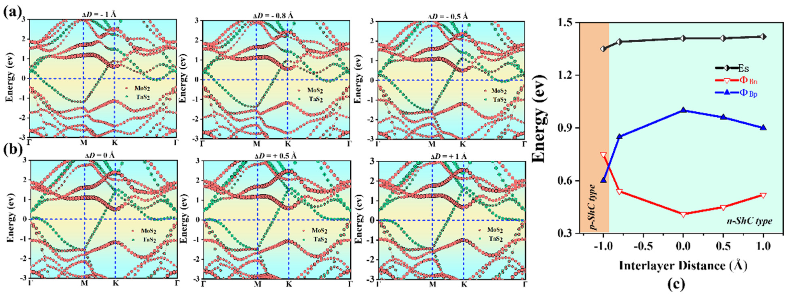
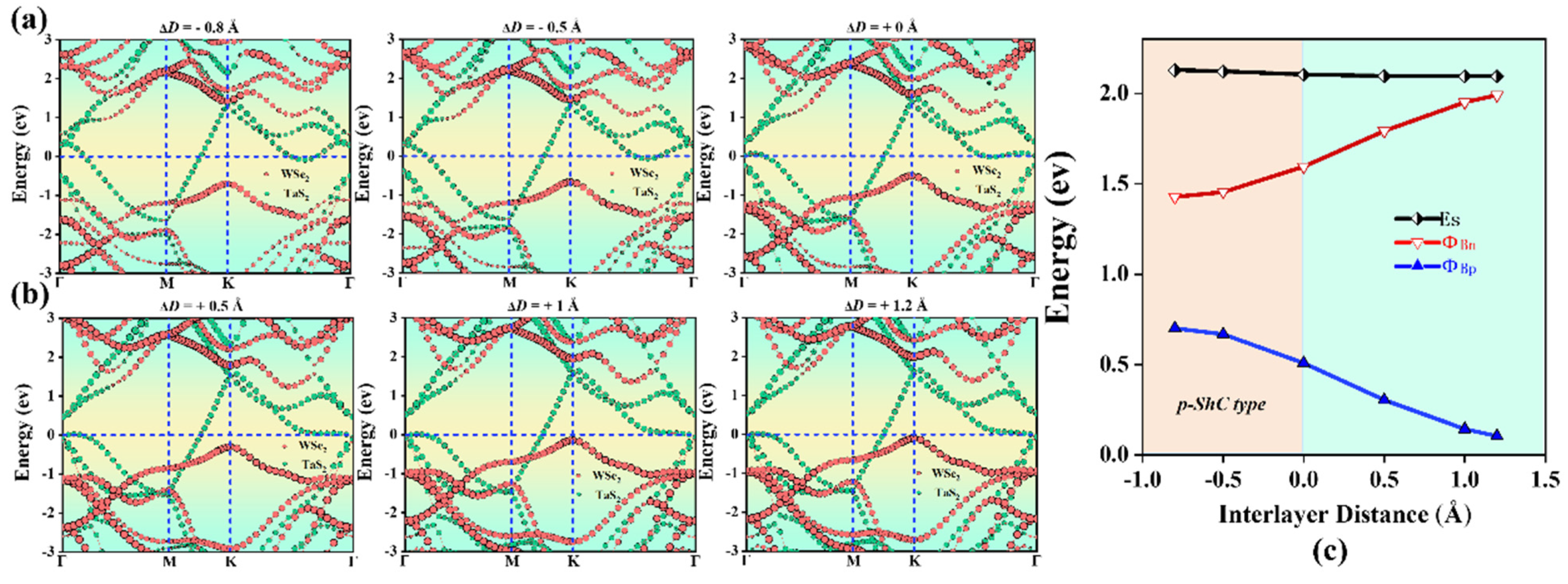
2.3. Heterostructures under Interlayer Distance

It is well known that applying mechanical strain to change interlayer coupling can adjust the interface properties of heterostructures. Controllable SBH and contact types in TaS2/MoS2(WSe2) vdWHs are one of the most important challenges to improve the performance of nanodevices. Therefore, we further investigate the effect of strain engineering by adjusting the interlayer distance and applied electric field. Furthermore, it is worth noting that the interlayer distance in 2D-based vdWHs can be controlled by scanning tunneling microscopy [52] or vacuum thermal annealing [53]. Here, the strain is applied by adjusting the layer spacing, defined as ΔD = D − D0, where the original D of MoS2 and WSe2 is 3.0 Å and 2.9 Å, respectively, and D0 is the layer spacing after the strain. The tensile strain is defined by increasing the interlayer distance D, while the compressive strain is defined by decreasing D. ΔD < 0 represents the compressive strain, while ΔD > 0 represents the tensile strain. As shown in Figure 6a,b, for TaS2/MoS2 vdWHs, it is found that the tensile strain tends to increase ΦBn and decrease ΦBp. In the case of ΔD > 0, the CBM of the MoS2 layer moves upward away from the Fermi level, resulting in the increase in ΦBn. On the other hand, VBM moves upward towards the Fermi level, resulting in a decrease in ΦBp. TaS2/MoS2 vdWHs changes with the SBH of ΔD, as shown in Figure 6c. When 0 < ΔD < 1 Å tensile strain, it can be seen that ΦBp > ΦBn. In this case, TaS2/MoS2 has the n-ShC type. Moreover, TaS2/MoS2 still maintains the n-ShC type under −0.8 < ΔD < 0 Å compression strain. However, when ΔD ≤ −0.8 Å, it is observed in Figure 6c that ΦBn is gradually larger than ΦBp, resulting in a transition from the n-ShC type to p-ShC type. Therefore, the SBH and contact types in TaS2/MoS2 vdWHs can be adjusted by changing the layer spacing. On the contrary, As shown in Figure 7a,b, for TaS2/WSe2 vdWHs, when ΔD is greater than −0.8 Å and less than 1.2 Å, according to the overall trend, we find that the WSe2 layer of the CBM moves upward away from the Fermi energy level, resulting in an increase in ΦBn. On the other hand, the VBM moves upward towards the Fermi level, resulting in a decrease in ΦBp. TaS2/WSe2 vdWHs changes with the SBH of ΔD, as shown in Figure 7c. It was observed that the SBH of TaS2/WSe2 vdWHs varied linearly with layer distance. When 0 < ΔD ≤ 1.2 Å tensile strain, it can be seen that ΦBn > ΦBp. In this case, TaS2/WSe2 has a p-ShC type. In addition, when −0.8 ≤ ΔD < 0 Å compressive strain, ΦBn is still larger than ΦBp. In this case, it indicates that TaS2/WSe2 still maintains the p-ShC type. Therefore, the SBH in TaS2/WSe2 vdWHs can be adjusted by changing the layer spacing, but the contact type cannot be adjusted.

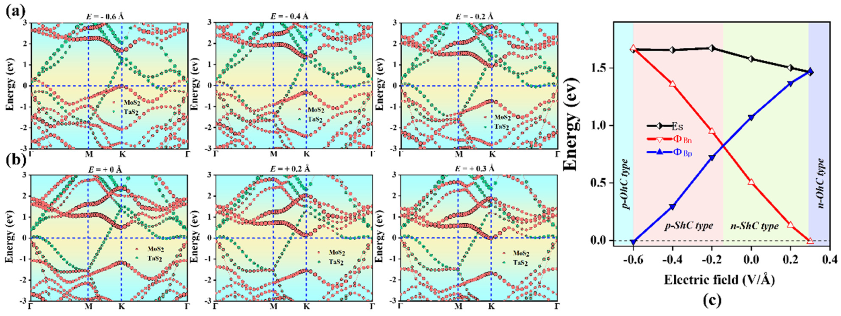
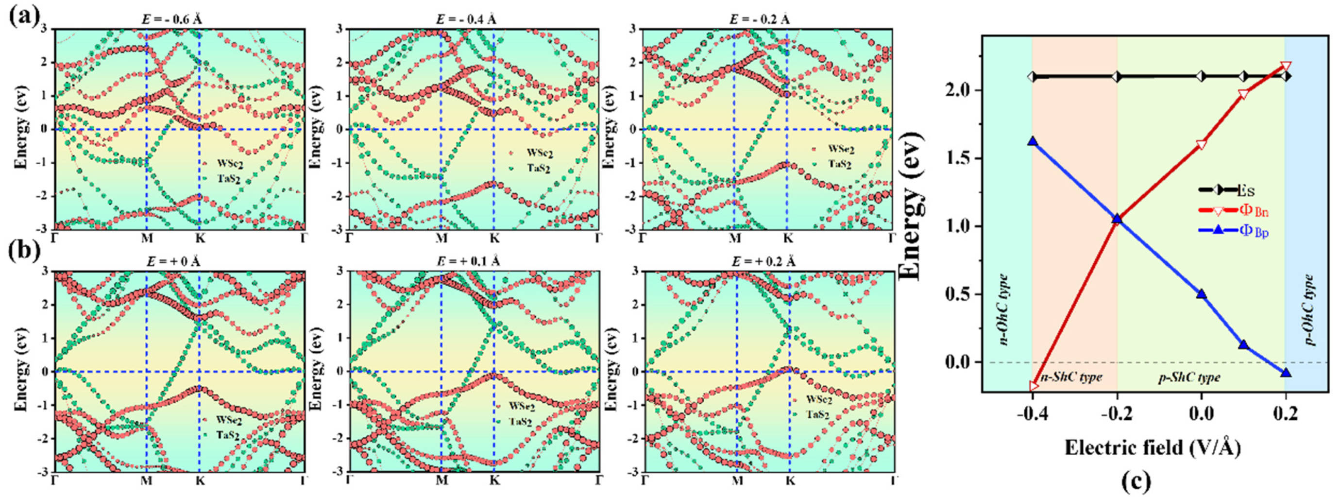
2.4. Heterostructures under Electric Field

Furthermore, we considered the effect of the electric field on the electronic properties and contact types of TaS2/MoS2 (WSe2) vdWHs, as shown in Figure 8 and Figure 9. It can be observed that the SBH of TaS2/MoS2 (WSe2) vdWHs changes linearly with the electric field. Here, the applied electric field is applied in the z direction of vdWHs. As shown in Figure 8a,b, for TaS2/MoS2 vdWHs, by applying a positive electric field, the CBM of the MoS2 layer moves down to the Fermi level, resulting in a decrease in ΦBn. Instead, VBM moves downward away from the Fermi level, causing ΦBp to increase. Interestingly, changes in SBH and contact types can be seen in Figure 8c. When a positive electric field of 0 < E < 0.3 V/Å is applied, it can be seen that ΦBp > ΦBn. In this case, the n-ShC type exists for 1T-TaS2/2H-MoS2 vdWHs. Surprisingly, when a positive electric field of E ≥ 0.3 V/Å is applied, it is found that the CBM of MoS2 moves down through the Fermi level and can form a transition from the n-ShC type to n-OhC type in TaS2/MoS2 vdWHs. Similarly, when a negative electric field of −0.14 < E ≤ 0 Å is applied, it can be found that ΦBp > ΦBn. In this case, the n-ShC type still exists for TaS2/MoS2 vdWHs. However, when a negative electric field of −0.6 < E ≤ −0.14 Å is applied, it can be observed that ΦBn is gradually larger than ΦBp, indicating that TaS2/MoS2 vdWHs can form a transition from the n-ShC type to p-ShC type. In addition, when a negative electric field of E ≤ −0.6 V/Å is applied, it can be found from the figure that the VBM of MoS2 moves upward through the Fermi level, forming a transition from the p-ShC type to p-OhC type. Similarly, as shown in Figure 9a,b, for TaS2/WSe2 vdWHs, the CBM of the WSe2 layer moves upward away from the Fermi level by applying a positive electric field, resulting in an increase in ΦBn. In contrast, VBM moves upward towards the Fermi level, resulting in a decrease in ΦBp.
Interestingly, changes in SBH and contact types can be seen in Figure 9c. When a positive electric field of 0 < E < 0.2 Å is applied, it can be seen that ΦBn > ΦBp. In this case, TaS2/WSe2 vdWHs will form the p-ShC type. Shockingly, when a positive electric field of E ≥ 0.2 Å was applied, the VBM of WSe2 was found to move upward through the Fermi level, forming a transition from the p-ShC type to p-OhC type. Furthermore, when a negative electric field −0.2 < E ≤ 0 Å is applied, it can be found that ΦBn > ΦBp. In this case, there is the p-ShC type in TaS2/WSe2 vdWHs. However, when a negative electric field of −0.4 < E ≤ −0.2 Å is applied, it can be found that ΦBp > ΦBn can form a transition from the p-ShC type to p-OhC type. Moreover, when a negative electric field of E ≤ −0.4 Å is applied, the CBM of WSe2 can be found to move down through the Fermi level, resulting in a transition from the n-ShC type to n-OhC type in TaS2/WSe2 vdWHs. All the above results indicate that the application of an electric field can regulate the contact type and SBH of TaS2/MoS2 (WSe2) vdWHs, as well as the conversion of Schottky contact to ohmic contact from the n-ShC type to p-ShC type. Our results can provide a new approach for the design of future electron nanodevices based on metal/semiconductor TaS2/MoS2 (WSe2) vdWHs.

3. Computational Methods

Structural optimization and property calculations are performed within the density functional theory framework [54], as implemented in the Vienna ab initio simulation package [55] (VASP), where the ion−electron interaction is implemented by the projector-augmented plane wave (PAW) approach [56]. The structural models, volumetric data such as electron/nuclear densities, and crystal morphologies are processed by Visualization for Electronic Structural Analysis [57] (VESTA). The electronic exchange-correlation functional is treated using the generalized gradient approximation [58] (GGA) in the form proposed by Perdew, Burke, and Ernzerhof [59] (PBE). The energy cutoff of the plane waves is set to 350 eV, with an energy precision of 10−6 eV. Atomic positions are fully relaxed until the force on each atom is less than 10−3 eV/Å. The supercell method is considered to simulate the monolayer, where a vacuum distance of ∼20 Å is used to eliminate the interaction between the adjacent layers. Considering that the GGA usually underestimates the bandgaps, we adopt the Heyd−Scuseria−Ernzerhof (HSE06) hybrid functional [60] to calculate the band structures. The dynamic stabilities and phonon dispersion curves are computed with the supercell approach, as implemented in the Phonopy code [61]. The dipole correction was also included in the calculations.

4. Conclusions

In summary, we investigated the electronic structure and interfacial properties of metal/semiconductor 1T-TaS2/2H-MoS2(2H-WSe2) vdWHs by using first-principles calculations. The metallic character of the monolayer 1T-TaS2 and the intrinsic properties of the monolayer 2H-MoS2(2H-WSe2) semiconductor are preserved in TaS2/MoS2(WSe2) vdWHs. We demonstrate that TaS2/MoS2 and TaS2/WSe2 form n-ShC type and p-ShC type Schottky contacts, with ultralow Schottky barrier heights (SBH) of 0.51 eV and 0.49 eV. The results show that TaS2 can be considered as an effective metal contact with high charge injection efficiency for MoS2, WSe2 semiconductors. Furthermore, the electronic structure and interfacial properties of TaS2/MoS2 (WSe2) vdWHs are tunable under the action of the strain and electric field, which can not only induce the change in SBH, but also form a transition from the n-ShC type to p-ShC type and from ShC to ohmic contacts. Our findings suggest that metal/semiconductor TaS2/MoS2(WSe2) vdWHs are promising candidates for optoelectronic devices.

Supplementary Materials

The following supporting information can be downloaded at: https://www.mdpi.com/article/10.3390/molecules28145607/s1. See the supplementary material for results of orientation-dependent Young’s modulus and Poisson’s ratio. Figure S1. Polar Plots of (a) Young’s modulus and (b) Poisson’s ratio of 1T-TaS2/2H-MoS2 vdWHs at the ground state. Polar Plots of (c) Young’s modulus and (d) Poisson’s ratio of 1T-TaS2/2H-WSe2 vdWHs at the ground state.

Author Contributions

Conceptualization, X.Q.; Investigation, X.Z., H.J., Y.Z., X.Q. and Y.L.; Data curation, X.Z., H.J. and Y.Z.; Writing—original draft preparation, X.Z.; Writing—review and editing, X.Q. and Y.L.; Visualization, X.Z.; Supervision, X.Q. and Y.L.; Funding acquisition, D.W., L.Y., L.F., Y.C., X.Q. and Y.L. All authors have read and agreed to the published version of the manuscript.

Funding

This research was funded by the Program for the National Natural Science Foundation of China (Grant No. 12204194), the Program for the Development of Science and Technology of Jilin Province (Grant No. YDZJ202101ZYTS065, 20220203021SF, YDZJ202301ZYTS244, 20210509050RQ, JJKH20220423KJ, YDZJ202201ZYTS308, YDZJ202201ZYTS307, 20210101409JC), and the Thirteenth Five-Year Program for Science and Technology of Education Department of Jilin Province (Grant No. JJKH20220425KJ). The Open Project of State Key Laboratory of Superhard Materials, Jilin University, (Grant No. 201908, 202306).

Institutional Review Board Statement

Not applicable.

Informed Consent Statement

Not applicable.

Data Availability Statement

Not applicable.

Conflicts of Interest

The authors declare no conflict of interest.

Sample Availability

Samples of the compounds are available from the authors upon request.

References

  1. Novoselov, K.S.; Fal′Ko, V.I.; Colombo, L.; Gellert, P.R.; Schwab, M.G.; Kim, K. A roadmap for graphene. Nature 2012, 490, 192–200. [Google Scholar] [CrossRef] [PubMed]
  2. Maisonneuve, P. Materials and Methods. Int. J. Gynecol. Obstet. 2006, 95, S5. [Google Scholar] [CrossRef] [PubMed]
  3. Novoselov, K.S.; Geim, A.K.; Morozov, S.V.; Jiang, D.; Katsnelson, M.I.; Grigorieva, I.V.; Dubonos, S.V.; Firsov, A.A. Two-dimensional gas of massless Dirac fermions in graphene. Nature 2005, 438, 197–200. [Google Scholar] [CrossRef] [Green Version]
  4. Geim, A.K.; Novoselov, K.S. The rise of graphene. In Nanoscience and Technology; World Scientific: Singapore, 2009; pp. 11–19. [Google Scholar]
  5. Malekpour, H.; Chang, K.-H.; Chen, J.-C.; Lu, C.-Y.; Nika, D.L.; Novoselov, K.S.; Balandin, A.A. Thermal Conductivity of Graphene Laminate. Nano Lett. 2014, 14, 5155–5161. [Google Scholar] [CrossRef] [PubMed]
  6. Novoselov, K.S.; Jiang, Z.; Zhang, Y.; Morozov, S.V.; Stormer, H.L.; Zeitler, U.; Maan, J.C.; Boebinger, G.S.; Kim, P.; Geim, A.K. Room-Temperature Quantum Hall Effect in Graphene. Science 2007, 315, 1379. [Google Scholar] [CrossRef] [PubMed] [Green Version]
  7. Mak, K.F.; Lee, C.; Hone, J.; Shan, J.; Heinz, T.F. Atomically ThinMoS2: A New Direct-Gap Semiconductor. Phys. Rev. Lett. 2010, 105, 136805. [Google Scholar] [CrossRef] [Green Version]
  8. Eknapakul, T.; King, P.D.C.; Asakawa, M.; Buaphet, P.; He, R.-H.; Mo, S.-K.; Takagi, H.; Shen, K.M.; Baumberger, F.; Sasagawa, T.; et al. Electronic Structure of a Quasi-Freestanding MoS2 Monolayer. Nano Lett. 2014, 14, 1312–1316. [Google Scholar] [CrossRef]
  9. Radisavljevic, B.; Radenovic, A.; Brivio, J.; Giacometti, V.; Kis, A. Single-layer MoS2 transistors. Nat. Nanotechnol. 2011, 6, 147–150. [Google Scholar] [CrossRef]
  10. Jena, D.; Konar, A. Enhancement of Carrier Mobility in Semiconductor Nanostructures by Dielectric Engineering. Phys. Rev. Lett. 2007, 98, 136805. [Google Scholar] [CrossRef] [Green Version]
  11. Yun, W.S.; Han, S.W.; Hong, S.C.; Kim, I.G.; Lee, J.D. Thickness and strain effects on electronic structures of transition metal dichalcogenides: 2H-MX2 semiconductors (M = Mo, W; X = S, Se, Te). Phys. Rev. B 2012, 85. [Google Scholar] [CrossRef]
  12. Ataca, C.; Ciraci, S. Functionalization of Single-Layer MoS2 Honeycomb Structures. J. Phys. Chem. C 2011, 115, 13303–13311. [Google Scholar] [CrossRef] [Green Version]
  13. Ataca, C.; Şahin, H.; Aktürk, E.; Ciraci, S. Mechanical and Electronic Properties of MoS2 Nanoribbons and Their Defects. J. Phys. Chem. C 2011, 115, 3934–3941. [Google Scholar] [CrossRef] [Green Version]
  14. Johari, P.; Shenoy, V.B. Tuning the Electronic Properties of Semiconducting Transition Metal Dichalcogenides by Applying Mechanical Strains. ACS Nano 2012, 6, 5449–5456. [Google Scholar] [CrossRef] [PubMed]
  15. Kumar, A.; Ahluwalia, P. A first principle Comparative study of electronic and optical properties of 1H – MoS2 and 2H – MoS2. Mater. Chem. Phys. 2012, 135, 755–761. [Google Scholar] [CrossRef]
  16. Scalise, E.; Houssa, M.; Pourtois, G.; Afanas’ev, V.; Stesmans, A. Strain-induced semiconductor to metal transition in the two-dimensional honeycomb structure of MoS2. Nano Res. 2011, 5, 43–48. [Google Scholar] [CrossRef]
  17. Li, Y.; Chen, Z. Tuning Electronic Properties of Germanane Layers by External Electric Field and Biaxial Tensile Strain: A Computational Study. J. Phys. Chem. C 2013, 118, 1148–1154. [Google Scholar] [CrossRef]
  18. Kumar, S.; Schwingenschlögl, U. Thermoelectric Response of Bulk and Monolayer MoSe2 and WSe2. Chem. Mater. 2015, 27, 1278–1284. [Google Scholar] [CrossRef]
  19. Cappelluti, E.; Roldán, R.; Silva-Guillén, J.A.; Ordejón, P.; Guinea, F. Tight-binding model and direct-gap/indirect-gap transition in single-layer and multilayer MoS2. Phys. Rev. B 2013, 88, 075409. [Google Scholar] [CrossRef] [Green Version]
  20. Lu, N.; Guo, H.; Wang, L.; Wu, X.; Zeng, X.C. van der Waals trilayers and superlattices: Modification of electronic structures of MoS2 by intercalation. Nanoscale 2014, 6, 4566–4571. [Google Scholar] [CrossRef] [Green Version]
  21. Kumar, S.; Kaczmarczyk, A.; Gerardot, B.D. Strain-Induced Spatial and Spectral Isolation of Quantum Emitters in Mono- and Bilayer WSe2. Nano Lett. 2015, 15, 7567–7573. [Google Scholar] [CrossRef] [Green Version]
  22. Fang, H.; Chuang, S.; Chang, T.C.; Takei, K.; Takahashi, T.; Javey, A. High-Performance Single Layered WSe2 p-FETs with Chemically Doped Contacts. Nano Lett. 2012, 12, 3788–3792. [Google Scholar] [CrossRef] [Green Version]
  23. Chuang, H.-J.; Tan, X.; Ghimire, N.J.; Perera, M.M.; Chamlagain, B.; Cheng, M.M.-C.; Yan, J.; Mandrus, D.; Tománek, D.; Zhou, Z. High Mobility WSe2 p- and n-Type Field-Effect Transistors Contacted by Highly Doped Graphene for Low-Resistance Contacts. Nano Lett. 2014, 14, 3594–3601. [Google Scholar] [CrossRef] [PubMed] [Green Version]
  24. Nourbakhsh, A.; Zubair, A.; Sajjad, R.N.; Tavakkoli, K.G.A.; Chen, W.; Fang, S.; Ling, X.; Kong, J.; Dresselhaus, M.S.; Kaxiras, E.; et al. MoS2 Field-Effect Transistor with Sub-10 nm Channel Length. Nano Lett. 2016, 16, 7798–7806. [Google Scholar] [CrossRef] [PubMed]
  25. Zhang, W.; Chiu, M.-H.; Chen, C.-H.; Chen, W.; Li, L.-J.; Wee, A.T.S. Role of Metal Contacts in High-Performance Phototransistors Based on WSe2 Monolayers. ACS Nano 2014, 8, 8653–8661. [Google Scholar] [CrossRef] [Green Version]
  26. Jeon, P.J.; Kim, J.S.; Lim, J.Y.; Cho, Y.; Pezeshki, A.; Lee, H.S.; Yu, S.; Min, S.-W.; Im, S. Low Power Consumption Complementary Inverters with n-MoS2 and p-WSe2 Dichalcogenide Nanosheets on Glass for Logic and Light-Emitting Diode Circuits. ACS Appl. Mater. Interfaces 2015, 7, 22333–22340. [Google Scholar] [CrossRef] [PubMed]
  27. Yu, L.; Zubair, A.; Santos, E.J.G.; Zhang, X.; Lin, Y.; Zhang, Y.; Palacios, T. High-Performance WSe2 Complementary Metal Oxide Semiconductor Technology and Integrated Circuits. Nano Lett. 2015, 15, 4928–4934. [Google Scholar] [CrossRef] [PubMed] [Green Version]
  28. Liu, B.; Luo, T.; Mu, G.; Wang, X.; Chen, D.; Shen, G. Rechargeable Mg-Ion Batteries Based on WSe2 Nanowire Cathodes. ACS Nano 2013, 7, 8051–8058. [Google Scholar] [CrossRef] [PubMed]
  29. Li, H.; Lu, G.; Wang, Y.; Yin, Z.; Cong, C.; He, Q.; Wang, L.; Ding, F.; Yu, T.; Zhang, H. Mechanical Exfoliation and Characterization of Single- and Few-Layer Nanosheets of WSe2, TaS2, and TaSe2. Small 2012, 9, 1974–1981. [Google Scholar] [CrossRef]
  30. Terrones, H.; Del Corro, E.; Feng, S.; Poumirol, J.M.; Rhodes, D.; Smirnov, D.; Pradhan, N.R.; Lin, Z.; Nguyen, M.A.T.; Elías, A.L.; et al. New First Order Raman-active Modes in Few Layered Transition Metal Dichalcogenides. Sci. Rep. 2014, 4, 4215. [Google Scholar] [CrossRef] [Green Version]
  31. Huang, J.; Yang, L.; Liu, D.; Chen, J.; Fu, Q.; Xiong, Y.; Lin, F.; Xiang, B. Large-area synthesis of monolayer WSe2 on a SiO2/Si substrate and its device applications. Nanoscale 2015, 7, 4193–4198. [Google Scholar] [CrossRef]
  32. Navarro-Moratalla, E.; Island, J.O.; Mañas-Valero, S.; Pinilla-Cienfuegos, E.; Castellanos-Gomez, A.; Quereda, J.; Rubio-Bollinger, G.; Chirolli, L.; Silva-Guillén, J.A.; Agraït, N.; et al. Enhanced superconductivity in atomically thin TaS2. Nat. Commun. 2016, 7, 11043. [Google Scholar] [CrossRef] [PubMed] [Green Version]
  33. Sharma, S.; Auluck, S.; Khan, M.A. Optical properties of 1T and 2H phase of TaS2 and TaSe2. Pramana 2000, 54, 431–440. [Google Scholar] [CrossRef]
  34. Shen, T.; Ren, J.-C.; Liu, X.; Li, S.; Liu, W. van der Waals Stacking Induced Transition from Schottky to Ohmic Contacts: 2D Metals on Multilayer InSe. J. Am. Chem. Soc. 2019, 141, 3110–3115. [Google Scholar] [CrossRef]
  35. Mohanta, M.K.; De Sarkar, A. 2D HfN2/graphene interface based Schottky device: Unmatched controllability in electrical contacts and carrier concentration via electrostatic gating and out-of-plane strain. Appl. Surf. Sci. 2020, 540, 148389. [Google Scholar] [CrossRef]
  36. Mohanta, M.K.; De Sarkar, A. Giant tunability in electrical contacts and doping via inconsiderable normal electric field strength or gating for a high-performance in ultrathin field effect transistors based on 2D BX/graphene (X = P, As) van der Waals heterobilayer. Appl. Surf. Sci. 2020, 526, 146749. [Google Scholar] [CrossRef]
  37. Wang, X.; Kim, S.Y.; Wallace, R.M. Interface Chemistry and Band Alignment Study of Ni and Ag Contacts on MoS2. ACS Appl. Mater. Interfaces 2021, 13, 15802–15810. [Google Scholar] [CrossRef] [PubMed]
  38. Dorow, C.; O’Brien, K.; Naylor, C.H.; Lee, S.; Penumatcha, A.; Hsiao, A.; Tronic, T.; Christenson, M.; Maxey, K.; Zhu, H.; et al. Advancing Monolayer 2-D nMOS and pMOS Transistor Integration From Growth to Van Der Waals Interface Engineering for Ultimate CMOS Scaling. IEEE Trans. Electron Devices 2021, 68, 6592–6598. [Google Scholar] [CrossRef]
  39. McDonnell, S.; Azcatl, A.; Addou, R.; Gong, C.; Battaglia, C.; Chuang, S.; Cho, K.; Javey, A.; Wallace, R.M. Hole Contacts on Transition Metal Dichalcogenides: Interface Chemistry and Band Alignments. ACS Nano 2014, 8, 6265–6272. [Google Scholar] [CrossRef]
  40. Gong, C.; Huang, C.; Miller, J.; Cheng, L.; Hao, Y.; Cobden, D.; Kim, J.; Ruoff, R.S.; Wallace, R.M.; Cho, K.; et al. Metal Contacts on Physical Vapor Deposited Monolayer MoS2. ACS Nano 2013, 7, 11350–11357. [Google Scholar] [CrossRef]
  41. Wang, Y.; Kim, J.C.; Li, Y.; Ma, K.Y.; Hong, S.; Kim, M.; Shin, H.S.; Jeong, H.Y.; Chhowalla, M. P-type electrical contacts for 2D transition-metal dichalcogenides. Nature 2022, 610, 61–66. [Google Scholar] [CrossRef]
  42. Wang, Y.; Kim, J.C.; Wu, R.J.; Martinez, J.; Song, X.; Yang, J.; Zhao, F.; Mkhoyan, A.; Jeong, H.Y.; Chhowalla, M. Van der Waals contacts between three-dimensional metals and two-dimensional semiconductors. Nature 2019, 568, 70–74. [Google Scholar] [CrossRef] [PubMed]
  43. Shen, P.-C.; Su, C.; Lin, Y.; Chou, A.-S.; Cheng, C.-C.; Park, J.-H.; Chiu, M.-H.; Lu, A.-Y.; Tang, H.-L.; Tavakoli, M.M.; et al. Ultralow contact resistance between semimetal and monolayer semiconductors. Nature 2021, 593, 211–217. [Google Scholar] [CrossRef] [PubMed]
  44. Xu, L.; Huang, W.-Q.; Hu, W.; Yang, K.; Zhou, B.-X.; Pan, A.; Huang, G.-F. Two-Dimensional MoS2-Graphene-Based Multilayer van der Waals Heterostructures: Enhanced Charge Transfer and Optical Absorption, and Electric-Field Tunable Dirac Point and Band Gap. Chem. Mater. 2017, 29, 5504–5512. [Google Scholar] [CrossRef] [Green Version]
  45. Sun, M.; Chou, J.-P.; Yu, J.; Tang, W. Effects of structural imperfection on the electronic properties of graphene/WSe2 heterostructures. J. Mater. Chem. C 2017, 5, 10383–10390. [Google Scholar] [CrossRef]
  46. Born, M.; Huang, K.; Lax, M. Dynamical Theory of Crystal Lattices. Am. J. Phys. 1955, 23, 474. [Google Scholar] [CrossRef]
  47. Mouhat, F.; Coudert, F.-X. Necessary and sufficient elastic stability conditions in various crystal systems. Phys. Rev. B 2014, 90. [Google Scholar] [CrossRef] [Green Version]
  48. He, C.; Cheng, M.; Li, T.T.; Zhang, W. Tunable Ohmic, p-Type Quasi-Ohmic, and n-Type Schottky Contacts of Monolayer SnSe with Metals. ACS Appl. Nano Mater. 2019, 2, 2767–2775. [Google Scholar] [CrossRef]
  49. Bardeen, J. Surface States and Rectification at a Metal Semi-Conductor Contact. Phys. Rev. 1947, 71, 717–727. [Google Scholar] [CrossRef]
  50. Zhang, W.X.; Yin, Y.; He, C. Spontaneous Enhanced Visible-Light-Driven Photocatalytic Water Splitting on Novel Type-II GaSe/CN and Ga2SSe/CN vdW Heterostructures. J. Phys. Chem. Lett. 2021, 12, 5064–5075. [Google Scholar] [CrossRef]
  51. He, C.; Liang, Y.; Zhang, W. Constructing a novel metal-free g-C3N4/g-CN vdW heterostructure with enhanced visible-light-driven photocatalytic activity for water splitting. Appl. Surf. Sci. 2021, 553, 149550. [Google Scholar] [CrossRef]
  52. Yankowitz, M.; Watanabe, K.; Taniguchi, T.; San-Jose, P.; LeRoy, B.J. Pressure-induced commensurate stacking of graphene on boron nitride. Nat. Commun. 2016, 7, 13168. [Google Scholar] [CrossRef] [PubMed] [Green Version]
  53. Tongay, S.; Fan, W.; Kang, J.; Park, J.; Koldemir, U.; Suh, J.; Narang, D.S.; Liu, K.; Ji, J.; Li, J.; et al. Tuning Interlayer Coupling in Large-Area Heterostructures with CVD-Grown MoS2 and WS2 Monolayers. Nano Lett. 2014, 14, 3185–3190. [Google Scholar] [CrossRef]
  54. Cohen, A.J.; Mori-Sánchez, P.; Yang, W. Challenges for Density Functional Theory. Chem. Rev. 2011, 112, 289–320. [Google Scholar] [CrossRef] [PubMed]
  55. Kresse, G.; Furthmüller, J. Efficient iterative schemes forab initiototal-energy calculations using a plane-wave basis set. Phys. Rev. B 1996, 54, 11169–11186. [Google Scholar] [CrossRef] [PubMed]
  56. Blöchl, P.E. Projector augmented-wave method. Phys. Rev. B 1994, 50, 17953–17979. [Google Scholar] [CrossRef] [Green Version]
  57. Momma, K.; Izumi, F. VESTA 3 for three-dimensional visualization of crystal, volumetric and morphology data. J. Appl. Crystallogr. 2011, 44, 1272–1276. [Google Scholar] [CrossRef]
  58. Perdew, J.P.; Burke, K.; Ernzerhof, M. Generalized gradient approximation made simple. Phys. Rev. Lett. 1996, 77, 3865–3868. [Google Scholar] [CrossRef] [Green Version]
  59. Paier, J.; Hirschl, R.; Marsman, M.; Kresse, G. The Perdew–Burke–Ernzerhof exchange-correlation functional applied to the G2-1 test set using a plane-wave basis set. J. Chem. Phys. 2005, 122, 234102. [Google Scholar] [CrossRef]
  60. Heyd, J.; Scuseria, G.E.; Ernzerhof, M. Hybrid functionals based on a screened Coulomb potential. J. Chem. Phys. 2003, 118, 8207–8215. [Google Scholar] [CrossRef] [Green Version]
  61. Togo, A.; Tanaka, I. First principles phonon calculations in materials science. Scr. Mater. 2015, 108, 1–5. [Google Scholar] [CrossRef] [Green Version]
Figure 1. (ac) show the optimized atomic structure (top view and side view), (df) phonon dispersion curve, (gi) HSE06 projected band structures and state density of 1T-TaS2, 2H-MoS2, 2H -WSe2, respectively. (jl) PBE projected band structures and state density of 1T-TaS2, 2H-MoS2, 2H -WSe2, respectively. The brown, yellow, purple, silver, and green balls represent tantalum, sulfur, molybdenum, tungsten, and selenium atoms, respectively.
Molecules 28 05607 g001
Figure 2. (a,b) Three different stacking forms of TaS2/MoS2, TaS2/WSe2 vdWHs, respectively. The brown, yellow, purple, silver, and green balls represent tantalum, sulfur, molybdenum, tungsten, and selenium atoms, respectively.
Molecules 28 05607 g002
Figure 3. (a,b) Weighted projected band structures of TaS2/MoS2, TaS2/WSe2 vdWHs obtained by PBE calculations, respectively. The blue, yellow, and green lines represent TaS2, MoS2, WSe2, respectively.
Molecules 28 05607 g003
Figure 4. (a,b) The work functions of TaS2, MoS2, WSe2 monolayer and their vdWHs.
Molecules 28 05607 g004
Figure 5. (a,b) In-plane average charge density difference of TaS2/MoS2, TaS2/WSe2 vdWHs, respectively. (c,d) In-plane average electrostatic potential of TaS2/MoS2, TaS2/WSe2 vdWHs, respectively. Inset represents the 3D charge density difference in the heterostructure. The yellow and cyan regions represent charge accumulation and depletion, respectively.
Molecules 28 05607 g005
Figure 6. Projected band structures of TaS2/MoS2 vdWHs at different interlayer distances in (a,b). The MoS2 and TaS2 layers in (a) are separated by red and green circles, respectively. (c) Evolution of the contact barrier in the TaS2/MoS2 heterostructure at different interlayer distances.
Molecules 28 05607 g006
Figure 7. Projected band structures of TaS2/WSe2 vdWHs at different interlayer distances in (a,b). The WSe2 and TaS2 layers in (a) are separated by red and green circles, respectively. (c) Evolution of the contact barrier in the TaS2/WSe2 heterostructure at different interlayer distances.
Molecules 28 05607 g007
Figure 8. Projected band structures of TaS2/MoS2 vdWHs along the z direction under different electric fields applied in (a,b). The MoS2 and TaS2 layers in (a) are separated by red and green circles, respectively. (c) Evolution of the contact barrier in the TaS2/MoS2 heterostructure under different electric fields.
Molecules 28 05607 g008
Figure 9. Projected band structures of TaS2/WSe2 vdWHs along the z direction under different electric fields applied in (a,b). The WSe2 and TaS2 layers in (a) are separated by red and green circles, respectively. (c) Evolution of the contact barrier in the TaS2/WSe2 heterostructure under different electric fields.
Molecules 28 05607 g009
Table 1. Calculated lattice parameters (a), interlayer distance (D), bandgap (Eg) obtained by PBE calculations, and effective mass for electrons (mex) and holes (mhy) along the x and y directions.
a (Å)D (Å)Eg (eV)mex/m0mhy/m0Contact Types
2H-MoS23.184_1.660.241.25_-
2H-WSe23.184_1.460.420.49_-
TaS2/WSe23.1862.91.63_-_-p-ShC
TaS2/MoS23.1863.01.58_-_-n-ShC
Disclaimer/Publisher’s Note: The statements, opinions and data contained in all publications are solely those of the individual author(s) and contributor(s) and not of MDPI and/or the editor(s). MDPI and/or the editor(s) disclaim responsibility for any injury to people or property resulting from any ideas, methods, instructions or products referred to in the content.

