

Various Applications of ZnO Thin Films Obtained by Chemical Routes in the Last Decade


Abstract
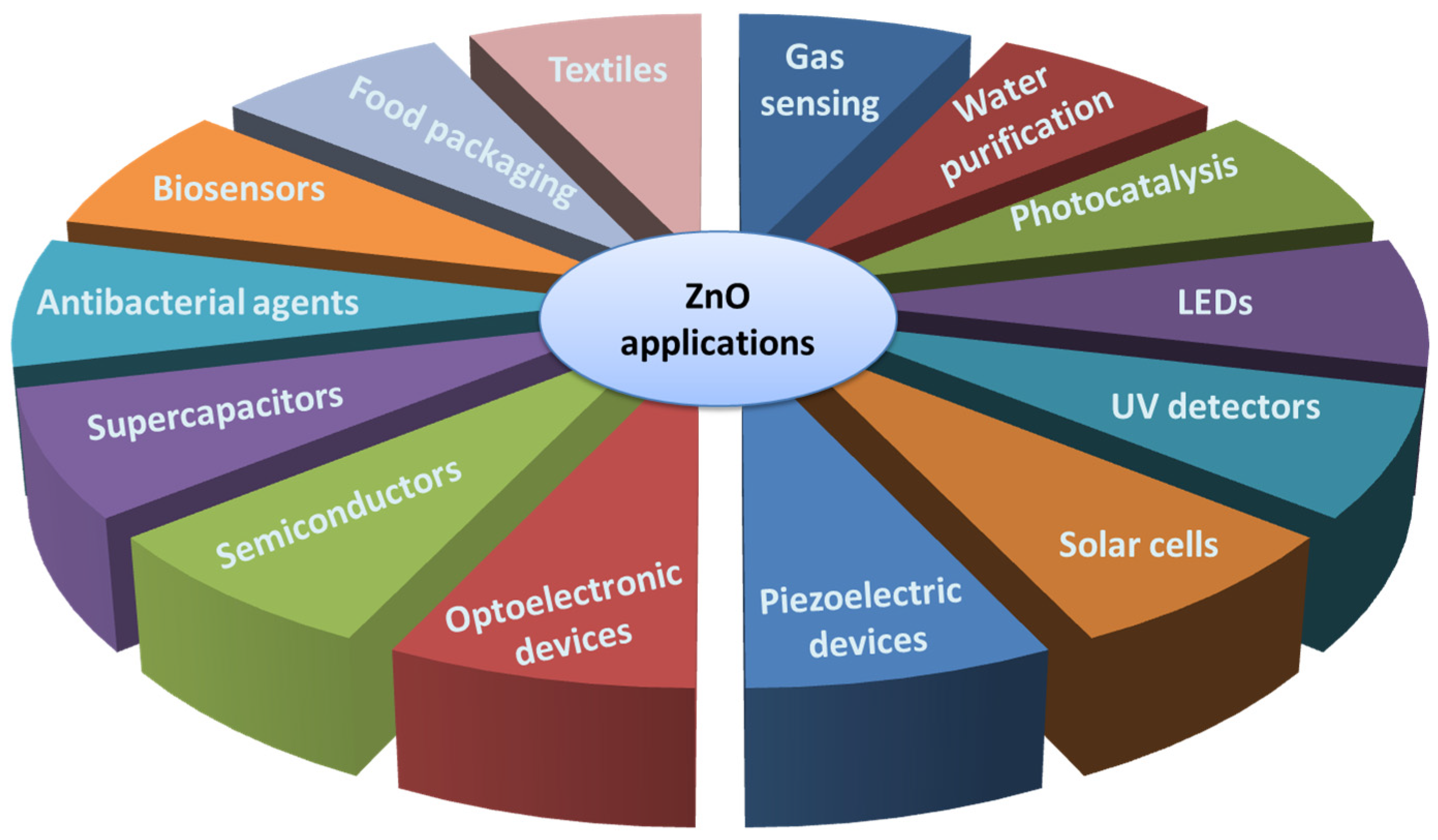
:1. Introduction
2. Preparation Methods of ZnO Films
2.1. Sol-Gel Synthesis
2.2. Hydrothermal Method
2.3. Chemical Bath Deposition
2.4. Successive Ionic Layer Adsorption and Reaction
2.5. Other Chemical Methods: Spray Pyrolysis, Inkjet Printing, Chemical Vapor Deposition (CVD)
3. ZnO as Seed Layer (SL)
4. ZnO in Composite Thin Films
5. Zn as Dopant
6. Doped and Codoped ZnO Films; p-Type Conductivity
7. Applications
7.1. Medical Field
7.2. Antibacterial Field
8. Summary, Conclusions, and Future Prospects
Author Contributions
Funding
Institutional Review Board Statement
Informed Consent Statement
Data Availability Statement
Acknowledgments
Conflicts of Interest
Abbreviations
| List of acronyms (in alphabetical order) | |
| AZO | Al-doped ZnO |
| BF | Bright field |
| CBD | Chemical Bath Deposition |
| CNFs | Ceramic nanofibers |
| CNT | Carbon nanotubes |
| CP | Conjugated polymer |
| CVD | Chemical Vapor Deposition |
| DMS | Dilute Magnetic Semiconductors |
| DSSCs | Dye-sensitized solar cells |
| EC | Ethylcellulose |
| ETL | Efficient electron transport layer |
| FET | Field effect transistors |
| HT | Hydrothermal synthesis |
| HPC | Hydroxypropyl cellulose |
| ITO | Indium Tin Oxide |
| LED | Light emitting diodes |
| NLO | Nonlinear optical properties |
| NG | Nanogenerator |
| NPs | Nanoparticles |
| NR | Nanorods |
| NWs | Nanowires |
| OFET | Organic field-effect transistor |
| PBTA | Poly(butylene adipate-co-terephthalate) |
| PDMS | Poly(dimethylsiloxane) |
| PDOS | Partial density of states |
| PEBA | Polyether block amide |
| PEI | Polyethyleneimine |
| PL | Photoluminescence |
| PLA | Polylactic acid |
| PP | Polypropylene |
| PVA | Poly(vinyl alcohol) |
| POPs | Persistent organic pollutants |
| RE | Rare earth |
| ROS | Reactive oxygen species |
| rGO | Reduced graphene |
| RhB | Rhodamine-B |
| SEM | Scanning Electron Microscopy |
| SG | Sol-Gel |
| SILAR | Successive Ionic Layer Adsorption and Reaction |
| SL | Seed Layer |
| TCO | Transparent Conductive Oxide |
| TEM | Transmission electron microscopy |
| TFT | Thin Film Transistors |
| UV | Ultraviolet |
| VOC | Volatile organic compound |
References
- Sharma, P.; Hasan, M.R.; Mehto, N.K.; Deepak; Bishoyi, A.; Narang, J. 92 years of zinc oxide: Has been studied by the scientific community since the 1930s- An overview. Sens. Int. 2022, 3, 100182. [Google Scholar] [CrossRef]
- Özgür, Ü.; Alivov, Y.I.; Liu, C.; Teke, A.; Reshchikov, M.A.; Doğan, S.; Avrutin, V.; Cho, S.-J.; Morkoç, H. A comprehensive review of ZnO materials and devices. J. Appl. Phys. 2005, 98, 041301. [Google Scholar] [CrossRef] [Green Version]
- Ellmer, K.; Klein, A. ZnO and Its Applications. In Transparent Conductive Zinc Oxide: Basics and Applications in Thin Film Solar Cells; Ellmer, K., Klein, A., Rech, B., Eds.; Springer: Berlin, Heidelberg, 2008; pp. 1–33. ISBN 978-3-540-73612-7. [Google Scholar]
- Borysiewicz, M.A. ZnO as a Functional Material, a Review. Crystals 2019, 9, 505. [Google Scholar] [CrossRef] [Green Version]
- Nowak, E.; Szybowicz, M.; Stachowiak, A.; Koczorowski, W.; Schulz, D.; Paprocki, K.; Fabisiak, K.; Los, S. A comprehensive study of structural and optical properties of ZnO bulk crystals and polycrystalline films grown by sol-gel method. Appl. Phys. A 2020, 126, 552. [Google Scholar] [CrossRef]
- Azarin, K.; Usatov, A.; Minkina, T.; Plotnikov, A.; Kasyanova, A.; Fedorenko, A.; Duplii, N.; Vechkanov, E.; Rajput, V.D.; Mandzhieva, S.; et al. Effects of ZnO nanoparticles and its bulk form on growth, antioxidant defense system and expression of oxidative stress related genes in Hordeum vulgare L. Chemosphere 2022, 287, 132167. [Google Scholar] [CrossRef]
- Qin, L.; Mawignon, F.J.; Hussain, M.; Ange, N.K.; Lu, S.; Hafezi, M.; Dong, G. Economic friendly zno-based uv sensors using hydrothermal growth: A review. Materials 2021, 14, 4083. [Google Scholar] [CrossRef] [PubMed]
- Theerthagiri, J.; Salla, S.; Senthil, R.A.; Nithyadharseni, P.; Madankumar, A.; Arunachalam, P.; Maiyalagan, T.; Kim, H.S. A review on ZnO nanostructured materials: Energy, environmental and biological applications. Nanotechnology 2019, 30, 392001. [Google Scholar] [CrossRef]
- Quynh, N.P.L.P.; Thi, T.U.D.; Tran, K.M.; Vu, H.N.; Ta, H.K.T.; Tran, C.V.; Phan, T.B.; Pham, N.K. Improving memory performance of PVA:ZnO nanocomposite: The experimental and theoretical approaches. Appl. Surf. Sci. 2021, 537, 148000. [Google Scholar] [CrossRef]
- Goktas, S.; Goktas, A. A comparative study on recent progress in efficient ZnO based nanocomposite and heterojunction photocatalysts: A review. J. Alloys Compd. 2021, 863, 158734. [Google Scholar] [CrossRef]
- Amari, R.; Mahroug, A.; Boukhari, A.; Deghfel, B.; Selmi, N. Structural, optical and luminescence properties of ZnO thin films prepared by sol-gel spin-coating method: Effect of precursor concentration. Chin. Phys. Lett. 2018, 35, 016801. [Google Scholar] [CrossRef]
- Elhosiny Ali, H.; Ganesh, V.; Haritha, L.; Aboraia, A.M.; Hegazy, H.H.; Butova, V.; Soldatov, A.V.; Algarni, H.; Guda, A.; Zahran, H.Y.; et al. Kramers-Kronig analysis of the optical linearity and nonlinearity of nanostructured Ga-doped ZnO thin films. Opt. Laser Technol. 2021, 135, 106691. [Google Scholar] [CrossRef]
- Bian, H.; Ma, S.; Yang, G.; Zhu, H.; Xu, X.; Yan, S.; Gao, J.; Zhang, Z. The optical and electrical properties of ZnO:Zr films. J. Alloys Compd. 2016, 672, 20–26. [Google Scholar] [CrossRef]
- Kumar, K.D.A.; Valanarasu, S.; Rosario, S.R.; Ganesh, V.; Shkir, M.; Sreelatha, C.J.; AlFaify, S. Evaluation of the structural, optical and electrical properties of AZO thin films prepared by chemical bath deposition for optoelectronics. Solid State Sci. 2018, 78, 58–68. [Google Scholar] [CrossRef]
- Podia, M.; Tripathi, A.K. Structural, optical and luminescence properties of ZnO thin films: Role of hot electrons defining the luminescence mechanisms. J. Lumin. 2022, 252, 119331. [Google Scholar] [CrossRef]
- Di Mauro, A.; Fragalà, M.E.; Privitera, V.; Impellizzeri, G. ZnO for application in photocatalysis: From thin films to nanostructures. Mater. Sci. Semicond. Process. 2017, 69, 44–51. [Google Scholar] [CrossRef]
- Gonçalves, R.S.; Barrozo, P.; Brito, G.L.; Viana, B.C.; Cunha, F. The effect of thickness on optical, structural and growth mechanism of ZnO thin film prepared by magnetron sputtering. Thin Solid Films 2018, 661, 40–45. [Google Scholar] [CrossRef]
- Speaks, D.T. Effect of concentration, aging, and annealing on sol gel ZnO and Al-doped ZnO thin films. Int. J. Mech. Mater. Eng. 2020, 15, 2. [Google Scholar] [CrossRef]
- Shaban, M.; Zayed, M.; Hamdy, H. Nanostructured ZnO thin films for self-cleaning applications. RSC Adv. 2017, 7, 617–631. [Google Scholar] [CrossRef]
- Zhang, Z.-Y.; Xiong, H.-M. Photoluminescent ZnO nanoparticles and their biological applications. Materials 2015, 8, 3101–3127. [Google Scholar] [CrossRef]
- Srivastava, A.K.; Tawale, J.S.; Verma, R.; Agarwal, D.; Sharma, C.; Kumar, A.; Gupta, M.K. Morphological evolution driven semiconducting nanostructures for emerging solar, biological and nanogenerator applications. Mater. Adv. 2022, 3, 8030–8062. [Google Scholar] [CrossRef]
- Manabeng, M.; Mwankemwa, B.S.; Ocaya, R.O.; Motaung, T.E.; Malevu, T.D. A Review of the Impact of Zinc Oxide Nanostructure Morphology on Perovskite Solar Cell Performance. Processes 2022, 10, 1803. [Google Scholar] [CrossRef]
- Wang, X.; Ahmad, M.; Sun, H. Three-dimensional ZnO hierarchical nanostructures: Solution phase synthesis and applications. Materials 2017, 10, 1304. [Google Scholar] [CrossRef] [PubMed] [Green Version]
- Galdámez-Martinez, A.; Santana, G.; Güell, F.; Martínez-Alanis, P.R.; Dutt, A. Photoluminescence of ZnO Nanowires: A Review. Nanomaterials 2020, 10, 857. [Google Scholar] [CrossRef]
- Noman, M.T.; Amor, N.; Petru, M. Synthesis and applications of ZnO nanostructures (ZONSs): A review. Crit. Rev. Solid State Mater. Sci. 2021, 47, 99–141. [Google Scholar] [CrossRef]
- Zhang, Y.; Ram, M.K.; Stefanakos, E.K.; Goswami, D.Y. Synthesis, Characterization, and Applications of ZnO Nanowires. J. Nanomater. 2012, 2012, 624520. [Google Scholar] [CrossRef] [Green Version]
- Liu, J.; Wang, Y.; Ma, J.; Peng, Y.; Wang, A. A review on bidirectional analogies between the photocatalysis and antibacterial properties of ZnO. J. Alloys Compd. 2019, 783, 898–918. [Google Scholar] [CrossRef]
- Kim, I.; Viswanathan, K.; Kasi, G.; Thanakkasaranee, S.; Sadeghi, K.; Seo, J. ZnO Nanostructures in Active Antibacterial Food Packaging: Preparation Methods, Antimicrobial Mechanisms, Safety Issues, Future Prospects, and Challenges. Food Rev. Int. 2022, 38, 537–565. [Google Scholar] [CrossRef] [Green Version]
- Indrajith Naik, E.; Sunil Kumar Naik, T.S.; Pradeepa, E.; Singh, S.; Naik, H.S.B. Design and fabrication of an innovative electrochemical sensor based on Mg-doped ZnO nanoparticles for the detection of toxic catechol. Mater. Chem. Phys. 2022, 281, 125860. [Google Scholar] [CrossRef]
- Ghosh, J.; Ghosh, R.; Giri, P.K. Tuning the visible photoluminescence in Al doped ZnO thin film and its application in label-free glucose detection. Sens. Actuators B Chem. 2018, 254, 681–689. [Google Scholar] [CrossRef]
- Sha, R.; Basak, A.; Maity, P.C.; Badhulika, S. ZnO nano-structured based devices for chemical and optical sensing applications. Sens. Actuators Repo. 2022, 4, 100098. [Google Scholar] [CrossRef]
- Yang, X.; Zhang, C.; Li, A.; Wang, J.; Cai, X. Red fluorescent ZnO nanoparticle grafted with polyglycerol and conjugated RGD peptide as drug delivery vehicles for efficient target cancer therapy. Mater. Sci. Eng. C 2019, 95, 104–113. [Google Scholar] [CrossRef]
- Rodrigues, J.; Pereira, S.O.; Zanoni, J.; Rodrigues, C.; Brás, M.; Costa, F.M.; Monteiro, T. ZnO Transducers for Photoluminescence-Based Biosensors: A Review. Chemosensors 2022, 10, 39. [Google Scholar] [CrossRef]
- Kumar, R.; Umar, A.; Kumar, G.; Nalwa, H.S. Antimicrobial properties of ZnO nanomaterials: A review. Ceram. Int. 2017, 43, 3940–3961. [Google Scholar] [CrossRef]
- Chen, X.; Xie, Q.; Li, J. Significantly improved photoluminescence properties of ZnO thin films by lithium doping. Ceram. Int. 2020, 46, 2309–2316. [Google Scholar] [CrossRef]
- Achehboune, M.; Khenfouch, M.; Boukhoubza, I.; Derkaoui, I.; Leontie, L.; Carlescu, A.; Mothudi, B.M.; Zorkani, I.; Jorio, A. Optimization of the luminescence and structural properties of Er-doped ZnO nanostructures: Effect of dopant concentration and excitation wavelength. J. Lumin. 2022, 246, 118843. [Google Scholar] [CrossRef]
- Chelouche, A.; Touam, T.; Necib, K.; Ouarez, L.; Challali, F.; Djouadi, D. Investigation of the effects of drying process on microstructural and luminescence properties of Al-doped ZnO thin films. J. Lumin. 2020, 219, 116891. [Google Scholar] [CrossRef]
- Narayanan, N.; Deepak, N.K. Enhancement of visible luminescence and photocatalytic activity of ZnO thin films via Cu doping. Optik 2018, 158, 1313–1326. [Google Scholar] [CrossRef]
- Musavi, E.; Khanlary, M.; Khakpour, Z. Red-orange photoluminescence emission of sol-gel dip-coated prepared ZnO and ZnO:Al nano-crystalline films. J. Lumin. 2019, 216, 116696. [Google Scholar] [CrossRef]
- Sandeep, K.M.; Bhat, S.; Dharmaprakash, S.M. Structural, optical, and LED characteristics of ZnO and Al doped ZnO thin films. J. Phys. Chem. Solids 2017, 104, 36–44. [Google Scholar] [CrossRef]
- Hasabeldaim, E.; Ntwaeaborwa, O.M.; Kroon, R.E.; Swart, H.C. Structural, optical and photoluminescence properties of Eu doped ZnO thin films prepared by spin coating. J. Mol. Struct. 2019, 1192, 105–114. [Google Scholar] [CrossRef]
- Shkir, M. Enhancement in optical and electrical properties of ZnO thin films via Co doping for photodetector applications. Mater. Sci. Eng. B 2022, 284, 115861. [Google Scholar] [CrossRef]
- Ambedkar, A.K.; Singh, M.; Kumar, V.; Kumar, V.; Singh, B.P.; Kumar, A.; Gautam, Y.K. Structural, optical and thermoelectric properties of Al-doped ZnO thin films prepared by spray pyrolysis. Surf. Interfaces 2020, 19, 100504. [Google Scholar] [CrossRef]
- Pham, A.T.T.; Ta, H.K.T.; Liu, Y.; Aminzare, M.; Wong, D.P.; Nguyen, T.H.; Pham, N.K.; Le, T.B.N.; Seetawan, T.; Ju, H.; et al. Effect of annealing temperature on thermoelectric properties of Ga and In dually doped—ZnO thin films. J. Alloys Compd. 2018, 747, 156–165. [Google Scholar] [CrossRef]
- Saini, S.; Mele, P.; Honda, H.; Suzuki, T.; Matsumoto, K.; Miyazaki, K.; Ichinose, A.; Molina Luna, L.; Carlini, R.; Tiwari, A. Effect of self-grown seed layer on thermoelectric properties of ZnO thin films. Thin Solid Films 2016, 605, 289–294. [Google Scholar] [CrossRef] [Green Version]
- Liu, S.; Li, G.; Xiao, L.; Jia, B.; Gao, Y.; Wang, Q. Effect of morphology evolution on the thermoelectric properties of oxidized ZnO thin films. Appl. Surf. Sci. 2018, 436, 354–361. [Google Scholar] [CrossRef]
- Chelu, M.; Stroescu, H.; Anastasescu, M.; Calderon-Moreno, J.M.; Preda, S.; Stoica, M.; Fogarassy, Z.; Petrik, P.; Gheorghe, M.; Parvulescu, C.; et al. High-quality PMMA/ZnO NWs piezoelectric coating on rigid and flexible metallic substrates. Appl. Surf. Sci. 2020, 529, 147135. [Google Scholar] [CrossRef]
- Tsay, C.-Y.; Hsu, W.-T. Comparative Studies on Ultraviolet-Light-Derived Photoresponse Properties of ZnO, AZO, and GZO Transparent Semiconductor Thin Films. Materials 2017, 10, 1379. [Google Scholar] [CrossRef] [Green Version]
- Bui, Q.C.; Salem, B.; Roussel, H.; Mescot, X.; Guerfi, Y.; Jiménez, C.; Consonni, V.; Ardila, G. Effects of thermal annealing on the structural and electrical properties of ZnO thin films for boosting their piezoelectric response. J. Alloys Compd. 2021, 870, 159512. [Google Scholar] [CrossRef]
- Goel, S.; Kumar, B. A review on piezo-/ferro-electric properties of morphologically diverse ZnO nanostructures. J. Alloys Compd. 2020, 816, 152491. [Google Scholar] [CrossRef]
- Pandey, R.K.; Dutta, J.; Brahma, S.; Rao, B.; Liu, C.P. Review on ZnO-based piezotronics and piezoelectric nanogenerators: Aspects of piezopotential and screening effect. J. Phys. Mater. 2021, 4, 044011. [Google Scholar] [CrossRef]
- Yue, R.; Ramaraj, S.G.; Liu, H.; Elamaran, D.; Elamaran, V.; Gupta, V.; Arya, S.; Verma, S.; Satapathi, S.; hayawaka, Y.; et al. A review of flexible lead-free piezoelectric energy harvester. J. Alloys Compd. 2022, 918, 165653. [Google Scholar] [CrossRef]
- Clementi, G.; Cottone, F.; Di Michele, A.; Gammaitoni, L.; Mattarelli, M.; Perna, G.; López-Suárez, M.; Baglio, S.; Trigona, C.; Neri, I. Review on Innovative Piezoelectric Materials for Mechanical Energy Harvesting. Energies 2022, 15, 6227. [Google Scholar] [CrossRef]
- Widyastuti, E.; Hsu, J.-L.; Lee, Y.-C. Insight on Photocatalytic and Photoinduced Antimicrobial Properties of ZnO Thin Films Deposited by HiPIMS through Thermal Oxidation. Nanomaterials 2022, 12, 463. [Google Scholar] [CrossRef]
- Piedade, A.P.; Pinho, A.C.; Branco, R.; Morais, P.V. Evaluation of antimicrobial activity of ZnO based nanocomposites for the coating of non-critical equipment in medical-care facilities. Appl. Surf. Sci. 2020, 513, 145818. [Google Scholar] [CrossRef]
- AL-Jawad, S.M.H.; Sabeeh, S.H.; Taha, A.A.; Jassim, H.A. Studying structural, morphological and optical properties of nanocrystalline ZnO:Ag films prepared by sol–gel method for antimicrobial activity. J. Sol-Gel Sci. Technol. 2018, 87, 362–371. [Google Scholar] [CrossRef]
- Kayani, Z.N.; Sahar, S.; Riaz, S.; Naseem, S. Tuning of optical and antibacterial characteristics of ZnO thin films: Role of Ce content. Ceram. Int. 2019, 45, 3930–3939. [Google Scholar] [CrossRef]
- Ekthammathat, N.; Thongtem, S.; Thongtem, T.; Phuruangrat, A. Characterization and antibacterial activity of nanostructured ZnO thin films synthesized through a hydrothermal method. Powder Technol. 2014, 254, 199–205. [Google Scholar] [CrossRef]
- Kaviyarasu, K.; Maria Magdalane, C.; Kanimozhi, K.; Kennedy, J.; Siddhardha, B.; Subba Reddy, E.; Rotte, N.K.; Sharma, C.S.; Thema, F.T.; Letsholathebe, D.; et al. Elucidation of photocatalysis, photoluminescence and antibacterial studies of ZnO thin films by spin coating method. J. Photochem. Photobiol. B Biol. 2017, 173, 466–475. [Google Scholar] [CrossRef] [PubMed]
- Bai, S.; Jin, Y.; Liang, X.; Ye, Z.; Wu, Z.; Sun, B.; Ma, Z.; Tang, Z.; Wang, J.; Würfel, U.; et al. Ethanedithiol Treatment of Solution-Processed ZnO Thin Films: Controlling the Intragap States of Electron Transporting Interlayers for Efficient and Stable Inverted Organic Photovoltaics. Adv. Energy Mater. 2015, 5, 1401606. [Google Scholar] [CrossRef] [Green Version]
- Das, D.; Mondal, P. Photoluminescence phenomena prevailing in c-axis oriented intrinsic ZnO thin films prepared by RF magnetron sputtering. RSC Adv. 2014, 4, 35735–35743. [Google Scholar] [CrossRef]
- Mia, M.N.H.; Pervez, M.F.; Hossain, M.K.; Reefaz Rahman, M.; Uddin, M.J.; Al Mashud, M.A.; Ghosh, H.K.; Hoq, M. Influence of Mg content on tailoring optical bandgap of Mg-doped ZnO thin film prepared by sol-gel method. Results Phys. 2017, 7, 2683–2691. [Google Scholar] [CrossRef]
- Ganesh, V.; Yahia, I.S.; AlFaify, S.; Shkir, M. Sn-doped ZnO nanocrystalline thin films with enhanced linear and nonlinear optical properties for optoelectronic applications. J. Phys. Chem. Solids 2017, 100, 115–125. [Google Scholar] [CrossRef]
- Xu, L.; Miao, J.; Chen, Y.; Su, J.; Yang, M.; Zhang, L.; Zhao, L.; Ding, S. Characterization of Ag-doped ZnO thin film for its potential applications in optoelectronic devices. Optik 2018, 170, 484–491. [Google Scholar] [CrossRef]
- Kumar, P.; Venu M, P.; Sandeep, K.M.; Shivadas Kindalkar, V.; Kote M, A.; Dharmaprakash, S.M. Non-polar a-plane oriented ZnO:Al thin films for optoelectronic applications. Phys. B Condens. Matter 2021, 606, 412721. [Google Scholar] [CrossRef]
- Qin, W.; Li, T.; Li, Y.; Qiu, J.; Ma, X.; Chen, X.; Hu, X.; Zhang, W. A high power ZnO thin film piezoelectric generator. Appl. Surf. Sci. 2016, 364, 670–675. [Google Scholar] [CrossRef]
- Fan, Q.; Li, D.; Li, J.; Wang, C. Structure and piezoelectricity properties of V-doped ZnO thin films fabricated by sol-gel method. J. Alloys Compd. 2020, 829, 154483. [Google Scholar] [CrossRef]
- Lee, P.-C.; Hsiao, Y.-L.; Dutta, J.; Wang, R.-C.; Tseng, S.-W.; Liu, C.-P. Development of porous ZnO thin films for enhancing piezoelectric nanogenerators and force sensors. Nano Energy 2021, 82, 105702. [Google Scholar] [CrossRef]
- Sarma, B.; Sarma, B.K. Role of residual stress and texture of ZnO nanocrystals on electro-optical properties of ZnO/Ag/ZnO multilayer transparent conductors. J. Alloys Compd. 2018, 734, 210–219. [Google Scholar] [CrossRef]
- Sharmin, A.; Tabassum, S.; Bashar, M.S.; Mahmood, Z.H. Depositions and characterization of sol–gel processed Al-doped ZnO (AZO) as transparent conducting oxide (TCO) for solar cell application. J. Theor. Appl. Phys. 2019, 13, 123–132. [Google Scholar] [CrossRef] [Green Version]
- Portillo-Cortez, K.; Islas, S.R.; Serrano-Lázaro, A.; Ortiz, A.; García-Sánchez, M.F.; Alonso, J.C.; Martínez, A.; Ramos, C.; Dutt, A.; Santana, G. A novel soft deposition methodology for textured ZnO:Al thin films as efficient transparent conductive oxide layers. Appl. Surf. Sci. Adv. 2022, 9, 100255. [Google Scholar] [CrossRef]
- Inamdar, S.I.; Rajpure, K.Y. High-performance metal-semiconductor-metal UV photodetector based on spray deposited ZnO thin films. J. Alloys Compd. 2014, 595, 55–59. [Google Scholar] [CrossRef]
- Rana, V.S.; Rajput, J.K.; Pathak, T.K.; Purohit, L.P. Multilayer MgZnO/ZnO thin films for UV photodetectors. J. Alloys Compd. 2018, 764, 724–729. [Google Scholar] [CrossRef]
- Omar, A.; Abdullah, H. Electron transport analysis in zinc oxide-based dye-sensitized solar cells: A review. Renew. Sustain. Energy Rev. 2014, 31, 149–157. [Google Scholar] [CrossRef]
- Kim, K.; Utashiro, K.; Abe, Y.; Kawamura, M. Structural Properties of Zinc Oxide Nanorods Grown on Al-Doped Zinc Oxide Seed Layer and Their Applications in Dye-Sensitized Solar Cells. Materials 2014, 7, 2522–2533. [Google Scholar] [CrossRef] [PubMed] [Green Version]
- Dhamodharan, P.; Manoharan, C.; Bououdina, M.; Venkadachalapathy, R.; Ramalingam, S. Al-doped ZnO thin films grown onto ITO substrates as photoanode in dye sensitized solar cell. Sol. Energy 2017, 141, 127–144. [Google Scholar] [CrossRef]
- Saranya, A.; Devasena, T.; Sivaram, H.; Jayavel, R. Role of hexamine in ZnO morphologies at different growth temperature with potential application in dye sensitized solar cell. Mater. Sci. Semicond. Process. 2019, 92, 108–115. [Google Scholar] [CrossRef]
- Ahmad, N.; Zhang, X.; Yang, S.; Zhang, D.; Wang, J.; uz Zafar, S.; Li, Y.; Zhang, Y.; Hussain, S.; Cheng, Z.; et al. Polydopamine/ZnO electron transport layers enhance charge extraction in inverted non-fullerene organic solar cells. J. Mater. Chem. C 2019, 7, 10795–10801. [Google Scholar] [CrossRef]
- Abdel-Galil, A.; Hussien, M.S.A.; Yahia, I.S. Synthesis and optical analysis of nanostructured F-doped ZnO thin films by spray pyrolysis: Transparent electrode for photocatalytic applications. Opt. Mater. 2021, 114, 110894. [Google Scholar] [CrossRef]
- Abdelkrim, M.; Guezzoul, M.; Bedrouni, M.; Bouslama, M.; Ouerdane, A.; Kharroubi, B. Effect of slight cobalt incorporation on the chemical, structural, morphological, optoelectronic, and photocatalytic properties of ZnO thin film. J. Alloys Compd. 2022, 920, 165703. [Google Scholar] [CrossRef]
- Tonezzer, M.; Le Dang, T.T.; Bazzanella, N.; Nguyen, V.H.; Iannotta, S. Comparative gas-sensing performance of 1D and 2D ZnO nanostructures. Sens. Actuators B Chem. 2015, 220, 1152–1160. [Google Scholar] [CrossRef]
- Shaikh, S.K.; Ganbavle, V.V.; Inamdar, S.I.; Rajpure, K.Y. Multifunctional zinc oxide thin films for high-performance UV photodetectors and nitrogen dioxide gas sensors. RSC Adv. 2016, 6, 25641–25650. [Google Scholar] [CrossRef]
- Kang, Y.; Yu, F.; Zhang, L.; Wang, W.; Chen, L.; Li, Y. Review of ZnO-based nanomaterials in gas sensors. Solid State Ion. 2021, 360, 115544. [Google Scholar] [CrossRef]
- Paliwal, A.; Sharma, A.; Tomar, M.; Gupta, V. Carbon monoxide (CO) optical gas sensor based on ZnO thin films. Sens. Actuators B Chem. 2017, 250, 679–685. [Google Scholar] [CrossRef]
- Hunge, Y.M.; Yadav, A.A.; Kulkarni, S.B.; Mathe, V.L. A multifunctional ZnO thin film based devices for photoelectrocatalytic degradation of terephthalic acid and CO2 gas sensing applications. Sens. Actuators B Chem. 2018, 274, 1–9. [Google Scholar] [CrossRef]
- Ghosh, A.; Zhang, C.; Shi, S.; Zhang, H. High temperature CO2 sensing and its cross-sensitivity towards H2 and CO gas using calcium doped ZnO thin film coated langasite SAW sensor. Sens. Actuators B Chem. 2019, 301, 126958. [Google Scholar] [CrossRef]
- Nimbalkar, A.R.; Patil, M.G. Synthesis of ZnO thin film by sol-gel spin coating technique for H2S gas sensing application. Phys. B Condens. Matter 2017, 527, 7–15. [Google Scholar] [CrossRef]
- Patil, V.L.; Vanalakar, S.A.; Patil, P.S.; Kim, J.H. Fabrication of nanostructured ZnO thin films based NO2 gas sensor via SILAR technique. Sens. Actuators B Chem. 2017, 239, 1185–1193. [Google Scholar] [CrossRef]
- Zhu, L.; Zeng, W. Room-temperature gas sensing of ZnO-based gas sensor: A review. Sens. Actuators A Phys. 2017, 267, 242–261. [Google Scholar] [CrossRef]
- da Silva, L.F.; M’Peko, J.-C.; Catto, A.C.; Bernardini, S.; Mastelaro, V.R.; Aguir, K.; Ribeiro, C.; Longo, E. UV-enhanced ozone gas sensing response of ZnO-SnO2 heterojunctions at room temperature. Sens. Actuators B Chem. 2017, 240, 573–579. [Google Scholar] [CrossRef] [Green Version]
- Jindal, K.; Tomar, M.; Gupta, V. A novel low-powered uric acid biosensor based on arrayed p-n junction heterostructures of ZnO thin film and CuO microclusters. Sen. Actuators B Chem. 2017, 253, 566–575. [Google Scholar] [CrossRef]
- Chakraborty, B.; Saha, R.; Chattopadhyay, S.; De, D.; Das, R.D.; Mukhopadhyay, M.K.; Palit, M.; RoyChaudhuri, C. Impact of surface defects in electron beam evaporated ZnO thin films on FET biosensing characteristics towards reliable PSA detection. Appl. Surf. Sci. 2021, 537, 147895. [Google Scholar] [CrossRef]
- Ogurcovs, A.; Kadiwala, K.; Sledevskis, E.; Krasovska, M.; Plaksenkova, I.; Butanovs, E. Effect of DNA Aptamer Concentration on the Conductivity of a Water-Gated Al:ZnO Thin-Film Transistor-Based Biosensor. Sensors 2022, 22, 3408. [Google Scholar] [CrossRef] [PubMed]
- Jung, H.J.; Lee, S.; Yu, Y.; Hong, S.M.; Choi, H.C.; Choi, M.Y. Low-temperature hydrothermal growth of ZnO nanorods on sol–gel prepared ZnO seed layers: Optimal growth conditions. Thin Solid Films 2012, 524, 144–150. [Google Scholar] [CrossRef]
- Predoana, L.; Stanciu, I.; Anastasescu, M.; Calderon-Moreno, J.M.; Stoica, M.; Preda, S.; Gartner, M.; Zaharescu, M. Structure and properties of the V-doped TiO2 thin films obtained by sol–gel and microwave-assisted sol–gel method. J. Sol-Gel Sci. Technol. 2016, 78, 589–599. [Google Scholar] [CrossRef]
- Nesheva, D.; Dzhurkov, V.; Stambolova, I.; Blaskov, V.; Bineva, I.; Calderon Moreno, J.M.; Preda, S.; Gartner, M.; Hristova-Vasileva, T.; Shipochka, M. Surface modification and chemical sensitivity of sol gel deposited nanocrystalline ZnO films. Mater. Chem. Phys. 2018, 209, 165–171. [Google Scholar] [CrossRef]
- Nagpal, V.J.; Davis, R.M.; Desu, S.B. Novel thin films of titanium dioxide particles synthesized by a sol-gel process. J. Mater. Res. 1995, 10, 3068–3078. [Google Scholar] [CrossRef]
- Stambolova, I.; Blaskov, V.; Shipochka, M.; Vassilev, S.; Dushkin, C.; Dimitriev, Y. Porous photocatalytically active ZnO films obtained from ethylcellulose modified solutions by spray pyrolysis. Mater. Chem. Phys. 2010, 121, 447–452. [Google Scholar] [CrossRef]
- Shankar, P.; Rayappan, J.B.B. Monomer: Design of ZnO nanostructures (nanobush and nanowire) and their room-temperature ethanol vapor sensing signatures. ACS Appl. Mater. Interfaces 2017, 9, 38135–38145. [Google Scholar] [CrossRef]
- Jang, M.; Lee, J.; Park, S.Y.; Lee, J.; Lee, K.M.; Song, W.; Myung, S.; Lee, S.S.; Jung, H.-K.; Kang, Y.C.; et al. Rational surface modification of ZnO with siloxane polymers for room-temperature-operated thin-film transistor-based gas sensors. Appl. Surf. Sci. 2021, 542, 148704. [Google Scholar] [CrossRef]
- Shin, S.Y.; Jang, M.; Cheon, H.J.; Go, S.; Yoon, H.; Chang, M. Nanostructure-assisted solvent vapor annealing of conjugated polymer thin films for enhanced performance in volatile organic compound sensing. Sens. Actuators B Chem. 2022, 351, 130951. [Google Scholar] [CrossRef]
- Wahid, K.A.; Rahim, I.A.; Safri, S.N.A.; Ariffin, A.H. Synthesis of ZnO nanorods at very low temperatures using ultrasonically pre-treated growth solution. Processes 2023, 11, 708. [Google Scholar] [CrossRef]
- Viter, R.; Fedorenko, V.; Gabriunaite, I.; Tepliakova, I.; Ramanavicius, S.; Holubnycha, V.; Ramanavicius, A.; Valiūnienė, A. Electrochemical and optical properties of fluorine doped tin oxide modified by ZnO nanorods and polydopamine. Chemosensors 2023, 11, 106. [Google Scholar] [CrossRef]
- Kamble, C.; Narwade, S.; Mane, R. Detection of acetylene (C2H2) gas using Ag-modified ZnO/GO nanorods prepared by a hydrothermal synthesis. Mater. Sci. Semicond. Process. 2023, 153, 107145. [Google Scholar] [CrossRef]
- Khayatian, A.; Asgari, V.; Ramazani, A.; Akhtarianfar, S.F.; Kashi, M.A.; Safa, S. Diameter-controlled synthesis of ZnO nanorods on Fe-doped ZnO seed layer and enhanced photodetection performance. Mater. Res. Bull. 2017, 94, 77–84. [Google Scholar] [CrossRef]
- Park, J.-S.; Mahmud, I.; Shin, H.J.; Park, M.-K.; Ranjkesh, A.; Lee, D.K.; Kim, H.-R. Effect of surface energy and seed layer annealing temperature on ZnO seed layer formation and ZnO nanowire growth. Appl. Surf. Sci. 2016, 362, 132–139. [Google Scholar] [CrossRef]
- Islavath, N.; Das, D.; Joshi, S.V.; Ramasamy, E. Seed layer-assisted low temperature solution growth of 3D ZnO nanowall architecture for hybrid solar cells. Mater. Des. 2017, 116, 219–226. [Google Scholar] [CrossRef]
- Banari, M.; Memarian, N.; Vomiero, A. Effect of the seed layer on the UV photodetection properties of ZnO nanorods. Mater. Sci. Eng. B 2021, 272, 115332. [Google Scholar] [CrossRef]
- Baig, F.; Asif, A.; Ashraf, M.W.; Imran, M. Comparative study for seed layer solvent effects on structural and optical properties of MgZnO thin films deposited by chemical bath deposition technique. Mater. Res. Express 2020, 7, 026417. [Google Scholar] [CrossRef]
- Hou, S.; Li, C. Aluminum-doped zinc oxide thin film as seeds layer effects on the alignment of zinc oxide nanorods synthesized in the chemical bath deposition. Thin Solid Films 2016, 605, 37–43. [Google Scholar] [CrossRef]
- Terasako, T.; Hamamoto, K.; Yagi, M.; Furubayashi, Y.; Yamamoto, T. Structural and photoluminescence properties of zinc oxide nanorods grown on various transparent conducting oxide seed layers by chemical bath deposition. Thin Solid Films 2021, 732, 138803. [Google Scholar] [CrossRef]
- Rezaie, M.N.; Manavizadeh, N.; Nayeri, F.D.; Bidgoli, M.M.; Nadimi, E.; Boroumand, F.A. Effect of seed layers on low-temperature, chemical bath deposited ZnO nanorods-based near UV-OLED performance. Ceram. Int. 2018, 44, 4937–4945. [Google Scholar] [CrossRef]
- Shaikh, S.K.; Inamdar, S.I.; Ganbavle, V.V.; Rajpure, K.Y. Chemical bath deposited ZnO thin film based UV photoconductive detector. J. Alloys Compd. 2016, 664, 242–249. [Google Scholar] [CrossRef]
- Nicolau, Y.F. Solution deposition of thin solid compound films by a successive ionic-layer adsorption and reaction process. Appl. Surf. Sci. 1985, 22–23, 1061–1074. [Google Scholar] [CrossRef]
- Ristov, M.; Sinadinovski, G.; Grozdanov, I. Chemical deposition of Cu2O thin films. Thin Solid Films 1985, 123, 63–67. [Google Scholar] [CrossRef]
- Yergaliuly, G.; Soltabayev, B.; Kalybekkyzy, S.; Bakenov, Z.; Mentbayeva, A. Effect of thickness and reaction media on properties of ZnO thin films by SILAR. Sci. Rep. 2022, 12, 851. [Google Scholar] [CrossRef]
- Galego, E.; Serna, M.M.; Ramanathan, L.V. A new route to grow ZnO seed layer using the SILAR method. In Technical Proceedings of the 2013 NSTI Nanotechnology Conference and Expo, NSTI-Nanotech 2013; CRC Press: Boca Raton, FL, USA, 2013; Volume 3, pp. 509–512. [Google Scholar]
- Kumar, K.D.A.; Valanarasu, S.; Ganesh, V.; Shkir, M.; Kathalingam, A.; AlFaify, S. Effect of precursors on key opto-electrical properties of successive ion layer adsorption and reaction-prepared Al:ZnO thin films. J. Electron. Mater. 2018, 47, 1335–1343. [Google Scholar] [CrossRef]
- Desai, M.A.; Sharma, V.; Prasad, M.; Jadkar, S.; Saratale, G.D.; Sartale, S.D. Seed-layer-free deposition of well-oriented ZnO nanorods thin films by SILAR and their photoelectrochemical studies. Int. J. Hydrogen Energy 2020, 45, 5783–5792. [Google Scholar] [CrossRef]
- Heitmann, U.; Westraadt, J.; O’Connell, J.; Jakob, L.; Dimroth, F.; Bartsch, J.; Janz, S.; Neethling, J. Spray Pyrolysis of ZnO:In: Characterization of Growth Mechanism and Interface Analysis on p-Type GaAs and n-Type Si Semiconductor Materials. ACS Appl. Mater. Interfaces 2022, 14, 41149–41155. [Google Scholar] [CrossRef]
- Saha, J.K.; Bukke, R.N.; Mude, N.N.; Jang, J. Significant improvement of spray pyrolyzed ZnO thin film by precursor optimization for high mobility thin film transistors. Sci. Rep. 2020, 10, 8999. [Google Scholar] [CrossRef]
- Rabeel, M.; Javed, S.; Khan, R.; Akram, M.A.; Rehman, S.; Kim, D.; Khan, M.F. Controlling the wettability of ZnO thin films by spray pyrolysis for photocatalytic applications. Materials 2022, 15, 3364. [Google Scholar] [CrossRef] [PubMed]
- Nurfani, E.; Lature, Y.K.; Anrokhi, M.S. Morphological modification and UV sensitivity enhancement in ZnO:Fe films with a seed layer. Opt. Mater. 2021, 122, 111658. [Google Scholar] [CrossRef]
- Vijayalakshmi, K.; Renitta, A. Enhanced H2 sensing performance presented by Mg doped ZnO films fabricated with a novel ITO seed layer. J. Mater. Sci. Mater. Electron. 2015, 26, 3458–3465. [Google Scholar] [CrossRef]
- Tran, V.-T.; Wei, Y.; Yang, H.; Zhan, Z.; Du, H. All-inkjet-printed flexible ZnO micro photodetector for a wearable UV monitoring device. Nanotechnology 2017, 28, 095204. [Google Scholar] [CrossRef] [PubMed]
- Vernieuwe, K.; Feys, J.; Cuypers, D.; De Buysser, K. Ink-Jet Printing of Aqueous Inks for Single-Layer Deposition of Al-Doped ZnO Thin Films. J. Am. Ceram. Soc. 2016, 99, 1353–1359. [Google Scholar] [CrossRef]
- Jiang, C.; Zhong, Z.; Liu, B.; He, Z.; Zou, J.; Wang, L.; Wang, J.; Peng, J.; Cao, Y. Coffee-ring-free quantum dot thin film using inkjet printing from a mixed-solvent system on modified ZnO transport layer for light-emitting devices. ACS Appl. Mater. Interfaces 2016, 8, 26162–26168. [Google Scholar] [CrossRef]
- Hoong, L.J.; Keat, Y.C.; Chik, A.; Leng, T.P. Band structure and thermoelectric properties of inkjet printed ZnO and ZnFe2O4 thin films. Ceram. Int. 2016, 42, 12064–12073. [Google Scholar] [CrossRef]
- Saini, S.; Mele, P.; Oyake, T.; Shiomi, J.; Niemelä, J.-P.; Karppinen, M.; Miyazaki, K.; Li, C.; Kawaharamura, T.; Ichinose, A.; et al. Porosity-tuned thermal conductivity in thermoelectric Al-doped ZnO thin films grown by mist-chemical vapor deposition. Thin Solid Films 2019, 685, 180–185. [Google Scholar] [CrossRef]
- Müller, R.; Huber, F.; Töws, M.; Mangold, M.; Madel, M.; Scholz, J.-P.; Minkow, A.; Herr, U.; Thonke, K. High-quality ZnO layers grown by CVD on sapphire substrates with an AlN nucleation layer. Cryst. Growth Des. 2020, 20, 3918–3926. [Google Scholar] [CrossRef]
- Kumar, S.; Sahare, P.D.; Kumar, S. Optimization of the CVD parameters for ZnO nanorods growth: Its photoluminescence and field emission properties. Mater. Res. Bull. 2018, 105, 237–245. [Google Scholar] [CrossRef]
- Sánchez-Martín, S.; Olaizola, S.M.; Castaño, E.; Urionabarrenetxea, E.; Mandayo, G.G.; Ayerdi, I. Study of deposition parameters and growth kinetics of ZnO deposited by aerosol assisted chemical vapor deposition. RSC Adv. 2021, 11, 18493–18499. [Google Scholar] [CrossRef] [PubMed]
- Choi, S.C.; Lee, D.K.; Sohn, S.H. Nano/micro-structured ZnO Rods synthesized by thermal chemical vapor deposition with perpendicularconfiguration. Nanomaterials 2021, 11, 2518. [Google Scholar] [CrossRef] [PubMed]
- Chalangar, E.; Nur, O.; Willander, M.; Gustafsson, A.; Pettersson, H. Synthesis of vertically aligned ZnO nanorods using sol-gel seeding and colloidal lithography patterning. Nanoscale Res. Lett. 2021, 16, 46. [Google Scholar] [CrossRef] [PubMed]
- Toe, M.Z.; Jusoh, N.A.H.N.; Pung, S.Y.; Yaacob, K.A.; Matsuda, A.; Tan, W.K.; Han, S.S. Effect of ZnO seed layer on the growth of ZnO nanorods on silicon substrate. Mater. Today Proc. 2019, 17, 553–559. [Google Scholar] [CrossRef]
- Basinova, N.; Cernohorsky, O.; Grym, J.; Kucerova, S.; Faitova, H.; Yatskiv, R.; Vanis, J.; Vesely, J.; Maixner, J. Highly textured seed layers for the growth of vertically oriented ZnO nanorods. Crystals 2019, 9, 566. [Google Scholar] [CrossRef] [Green Version]
- Zhang, C. High-quality oriented ZnO films grown by sol–gel process assisted with ZnO seed layer. J. Phys. Chem. Solids 2010, 71, 364–369. [Google Scholar] [CrossRef]
- Bašinová, N.; Černohorský, O.; Grym, J.; Maixner, J. Effect of heat treatment on the properties of sol-gel deposited ZnO seed layers. In Proceedings of the NANOCON 2017—Conference Proceedings, 9th International Conference on Nanomaterials—Research and Application, Brno, Czech Republic, 18–20 October 2017; pp. 128–133. [Google Scholar]
- Al-She’irey, A.Y.; Balouch, A.; Mawarnis, E.R.; Roza, L.; Rahman, M.Y.A.; Abdullah; Mahar, A.M. Effect of ZnO seed layer annealing temperature on the growth of ZnO nanorods and its catalytic application. Opt. Mater. 2022, 131, 112652. [Google Scholar] [CrossRef]
- Pimentel, A.; Ferreira, S.; Nunes, D.; Calmeiro, T.; Martins, R.; Fortunato, E. Microwave synthesized ZnO nanorod arrays for UV Sensors: A seed layer annealing temperature study. Materials 2016, 9, 299. [Google Scholar] [CrossRef] [Green Version]
- Azmi, Z.H.; Mohd Aris, S.N.; Abubakar, S.; Sagadevan, S.; Siburian, R.; Paiman, S. Effect of seed layer on the growth of zinc oxide nanowires by chemical bath deposition method. Coatings 2022, 12, 474. [Google Scholar] [CrossRef]
- Singh, P.; Simanjuntak, F.M.; Hu, L.-L.; Tseng, T.-Y.; Zan, H.-W.; Chu, J.P. Negative effects of annealed seed layer on the performance of ZnO-nanorods based nitric oxide gas sensor. Sensors 2022, 22, 390. [Google Scholar] [CrossRef] [PubMed]
- Leonardi, S. Two-dimensional zinc oxide nanostructures for gas sensor applications. Chemosensors 2017, 5, 17. [Google Scholar] [CrossRef] [Green Version]
- Ao, D.; Li, Z.; Fu, Y.; Tang, Y.; Yan, S.; Zu, X. Heterostructured NiO/ZnO Nanorod Arrays with Significantly Enhanced H2S Sensing Performance. Nanomaterials 2019, 9, 900. [Google Scholar] [CrossRef] [Green Version]
- Dey, S.; Nag, S.; Santra, S.; Ray, S.K.; Guha, P.K. Voltage-controlled NiO/ZnO p–n heterojunction diode: A new approach towards selective VOC sensing. Microsyst. Nanoeng. 2020, 6, 35. [Google Scholar] [CrossRef]
- Zhao, Z.; Yang, H.; Wei, Z.; Xue, Y.; Sun, Y.; Zhang, W.; Li, P.; Gong, W.; Zhuiykov, S.; Hu, J. NH3 Sensor Based on 3D Hierarchical Flower-Shaped n-ZnO/p-NiO Heterostructures Yields Outstanding Sensing Capabilities at ppb Level. Sensors 2020, 20, 4754. [Google Scholar] [CrossRef] [PubMed]
- Chelu, M.; Chesler, P.; Anastasescu, M.; Hornoiu, C.; Mitrea, D.; Atkinson, I.; Brasoveanu, C.; Moldovan, C.; Craciun, G.; Gheorghe, M.; et al. ZnO/NiO heterostructure-based microsensors used in formaldehyde detection at room temperature: Influence of the sensor operating voltage. J. Mater. Sci. Mater. Electron. 2022, 33, 19998–20011. [Google Scholar] [CrossRef]
- Umar, A.; Ibrahim, A.A.; Kumar, R.; Algadi, H.; Albargi, H.; Alsairi, M.A.; Alhmami, M.A.M.; Zeng, W.; Ahmed, F.; Akbar, S. CdO–ZnO nanorices for enhanced and selective formaldehyde gas sensing applications. Environ. Res. 2021, 200, 111377. [Google Scholar] [CrossRef] [PubMed]
- Liu, J.; Chen, Y.; Zhang, H. Study of Highly Sensitive Formaldehyde Sensors Based on ZnO/CuO Heterostructure via the Sol-Gel Method. Sensors 2021, 21, 4685. [Google Scholar] [CrossRef]
- Ghosh, A.; Bhowmick, T.; Majumder, S.B. Multi-layered zinc oxide-graphene composite thin films for selective nitrogen dioxide sensing. J. Appl. Phys. 2018, 123, 084501. [Google Scholar] [CrossRef]
- Wu, J.; Gong, M. ZnO/graphene heterostructure nanohybrids for optoelectronics and sensors. J. Appl. Phys. 2021, 130, 070905. [Google Scholar] [CrossRef]
- Muchtar, A.R.; Septiani, N.L.W.; Iqbal, M.; Nuruddin, A.; Yuliarto, B. Preparation of Graphene–Zinc Oxide Nanostructure Composite for Carbon Monoxide Gas Sensing. J. Electron. Mater. 2018, 47, 3647–3656. [Google Scholar] [CrossRef]
- Chesler, P.; Hornoiu, C.; Mihaiu, S.; Vladut, C.; Calderon Moreno, J.M.; Anastasescu, M.; Moldovan, C.; Firtat, B.; Brasoveanu, C.; Muscalu, G.; et al. Nanostructured SnO 2 –ZnO composite gas sensors for selective detection of carbon monoxide. Beilstein J. Nanotechnol. 2016, 7, 2045–2056. [Google Scholar] [CrossRef] [PubMed] [Green Version]
- Yang, X.; Zhang, S.; Yu, Q.; Zhao, L.; Sun, P.; Wang, T.; Liu, F.; Yan, X.; Gao, Y.; Liang, X.; et al. One step synthesis of branched SnO2/ZnO heterostructures and their enhanced gas-sensing properties. Sens. Actuators B Chem. 2019, 281, 415–423. [Google Scholar] [CrossRef]
- Tharsika, T.; Thanihaichelvan, M.; Haseeb, A.S.M.A.; Akbar, S.A. Highly Sensitive and Selective Ethanol Sensor Based on ZnO Nanorod on SnO2 Thin Film Fabricated by Spray Pyrolysis. Front. Mater. 2019, 6, 122. [Google Scholar] [CrossRef] [Green Version]
- Wang, T.; Liu, B.; Li, Q.; Wang, S. Controllable construction of Cr2O3-ZnO hierarchical heterostructures and their formaldehyde gas sensing properties. Mater. Lett. 2018, 221, 260–263. [Google Scholar] [CrossRef]
- Bao, Q.; Zhang, H.; Wang, Y.; Ni, Z.; Yan, Y.; Shen, Z.X.; Loh, K.P.; Tang, D.Y. Atomic-layer graphene as a saturable absorber for ultrafast pulsed lasers. Adv. Funct. Mater. 2009, 19, 3077–3083. [Google Scholar] [CrossRef]
- Chan, S.W.; Barille, R.; Nunzi, J.M.; Tam, K.H.; Leung, Y.H.; Chan, W.K.; Djurišić, A.B. Second harmonic generation in zinc oxide nanorods. Appl. Phys. B Lasers Opt. 2006, 84, 351–355. [Google Scholar] [CrossRef]
- Petrov, G.I.; Shcheslavskiy, V.; Yakovlev, V.V.; Ozerov, I.; Chelnokov, E.; Marine, W. Efficient third-harmonic generation in a thin nanocrystalline film of ZnO. Appl. Phys. Lett. 2003, 83, 3993–3995. [Google Scholar] [CrossRef] [Green Version]
- Sreeja, V.G.; Hajara, P.; Reshmi, R.; Anila, E.I. Effects of reduced graphene oxide on nonlinear absorption and optical limiting properties of spin coated aluminium doped zinc oxide thin films. Thin Solid Films 2021, 722, 138580. [Google Scholar] [CrossRef]
- Jia, X.; Wu, N.; Wei, J.; Zhang, L.; Luo, Q.; Bao, Z.; Li, Y.-Q.; Yang, Y.; Liu, X.; Ma, C.-Q. A low-cost and low-temperature processable zinc oxide-polyethylenimine (ZnO:PEI) nano-composite as cathode buffer layer for organic and perovskite solar cells. Org. Electron. 2016, 38, 150–157. [Google Scholar] [CrossRef]
- Kang, B.-C.; Park, S.-J.; Ha, T.-J. Wearable pressure/touch sensors based on hybrid dielectric composites of zinc oxide nanowires/poly(dimethylsiloxane) and flexible electrodes of immobilized carbon nanotube random networks. ACS Appl. Mater. Interfaces 2021, 13, 42014–42023. [Google Scholar] [CrossRef] [PubMed]
- Drakakis, E.; Suchea, M.; Tudose, V.; Kenanakis, G.; Stratakis, D.; Dangakis, K.; Miaoudakis, A.; Vernardou, D.; Koudoumas, E. Zinc oxide-graphene based composite layers for electromagnetic interference shielding in the GHz frequency range. Thin Solid Films 2018, 651, 152–157. [Google Scholar] [CrossRef]
- Hsieh, G.-W.; Ling, S.-R.; Hung, F.-T.; Kao, P.-H.; Liu, J.-B. Enhanced piezocapacitive response in zinc oxide tetrapod–poly(dimethylsiloxane) composite dielectric layer for flexible and ultrasensitive pressure sensor. Nanoscale 2021, 13, 6076–6086. [Google Scholar] [CrossRef] [PubMed]
- Venkatesh, C.; Clear, O.; Major, I.; Lyons, J.G.; Devine, D.M. Faster release of lumen-loaded drugs than matrix-loaded equivalent in polylactic acid/halloysite nanotubes. Materials 2019, 12, 1830. [Google Scholar] [CrossRef] [PubMed] [Green Version]
- Venkatesh, C.; Laurenti, M.; Bandeira, M.; Lanzagorta, E.; Lucherini, L.; Cauda, V.; Devine, D. Biodegradation and antimicrobial properties of zinc oxide–polymer composite materials for urinary stent applications. Coatings 2020, 10, 1002. [Google Scholar] [CrossRef]
- Venkatesan, R.; Rajeswari, N. ZnO/PBAT nanocomposite films: Investigation on the mechanical and biological activity for food packaging. Polym. Adv. Technol. 2017, 28, 20–27. [Google Scholar] [CrossRef]
- Chen, H.-C.; Lin, S.-W.; Jiang, J.-M.; Su, Y.-W.; Wei, K.-H. Solution-processed zinc oxide/polyethylenimine nanocomposites as tunable electron transport layers for highly efficient bulk heterojunction polymer solar cells. ACS Appl. Mater. Interfaces 2015, 7, 6273–6281. [Google Scholar] [CrossRef]
- Xu, X.; Shukla, S.; Liu, Y.; Yue, B.; Bullock, J.; Su, L.; Li, Y.; Javey, A.; Fang, X.; Ager, J.W. Solution-processed transparent self-powered p-CuS-ZnS/n-ZnO UV photodiode. Phys. Status Solidi—Rapid Res. Lett. 2018, 12, 1700381. [Google Scholar] [CrossRef] [Green Version]
- Ho Kim, K. Incorporation of Co2+, Cu2+, and Zn2+ ions into nickel oxide thin films and their enhanced electrochemical and electrochromic performances. Int. J. Electrochem. Sci. 2022, 17, 220125. [Google Scholar] [CrossRef]
- Mansoor, S.; Shahid, S.; Ashiq, K.; Alwadai, N.; Javed, M.; Iqbal, S.; Fatima, U.; Zaman, S.; Nazim Sarwar, M.; Alshammari, F.H.; et al. Controlled growth of nanocomposite thin layer based on Zn-doped MgO nanoparticles through sol-gel technique for biosensor applications. Inorg. Chem. Commun. 2022, 142, 109702. [Google Scholar] [CrossRef]
- Gartner, M.; Anastasescu, M.; Calderon-Moreno, J.M.; Nicolescu, M.; Stroescu, H.; Hornoiu, C.; Preda, S.; Predoana, L.; Mitrea, D.; Covei, M.; et al. Multifunctional Zn-doped ITO sol–gel films deposited on different substrates: Application as CO2-sensing material. Nanomaterials 2022, 12, 3244. [Google Scholar] [CrossRef] [PubMed]
- Okhay, O.; Vilarinho, P.M.; Tkach, A. Low-temperature dielectric response of strontium titanate thin films manipulated by Zn doping. Materials 2022, 15, 859. [Google Scholar] [CrossRef] [PubMed]
- Ghemid, M.; Gueddaoui, H.; Brahimi, R.; Trari, M. Simple and effective synthesis via sol–gel of Zn-doped ITO films and their microstructural, optical, and photoelectrochemical properties. Appl. Phys. A 2022, 128, 816. [Google Scholar] [CrossRef]
- Benhamida, S.; Gouamid, M.; Tlili, S.; Khenblouche, A.; Charradi, K. Structural, optical and dielectric properties of Zn-doped NiO thin films synthesized via sol-gel route. Dig. J. Nanomater. Biostruct. 2021, 16, 433–442. [Google Scholar] [CrossRef]
- Yang, S.; Zhang, F.; Xie, X.; Sun, H.; Zhang, L.; Fan, S. Enhanced leakage and ferroelectric properties of Zn-doped BiFeO3 thin films grown by sol-gel method. J. Alloys Compd. 2018, 734, 243–249. [Google Scholar] [CrossRef]
- Samarasekara, P.; Karunarathna, P.G.D.C.K.; Weeramuni, H.P.; Fernando, C.A.N. Characterization of spin coated Zn doped cupric oxide thin films. arXiv 2018, arXiv:1802.02886. [Google Scholar]
- Yang, S.; Zhang, F.; Xie, X.; Guo, X.; Zhang, L.; Fan, S. Effects of transition metal (Cu, Zn, Mn) doped on leakage current and ferroelectric properties of BiFeO3 thin films. J. Mater. Sci. Mater. Electron. 2017, 28, 14944–14948. [Google Scholar] [CrossRef]
- Raj, I.L.P.; Valanarasu, S.; Ade, R.; Bitla, Y.; Mohanraj, P.; Ganesh, V.; Yahia, I.S. Enhancing the ultraviolet photosensing properties of nickel oxide thin films by Zn–La co-doping. Ceram. Int. 2022, 48, 5026–5034. [Google Scholar] [CrossRef]
- Badawi, A.; Althobaiti, M.G.; Alharthi, S.S.; Alharbi, A.N.; Alkathiri, A.A.; Alomairy, S.E. Effect of zinc doping on the structure and optical properties of iron oxide nanostructured films prepared by spray pyrolysis technique. Appl. Phys. A 2022, 128, 123. [Google Scholar] [CrossRef]
- Shkir, M.; Anis, M.; Shafik, S.; Manthrammel, M.A.; Sayeed, M.A.; Hamdy, M.S.; AlFaify, S. An effect of Zn content doping on opto-third order nonlinear characteristics of nanostructured CdS thin films fabricated through spray pyrolysis for optoelectronics. Phys. E Low-Dimens. Syst. Nanostruct. 2020, 118, 113955. [Google Scholar] [CrossRef]
- Nesa, M.; Sharmin, M.; Hossain, K.S.; Bhuiyan, A.H. Structural, morphological, optical and electrical properties of spray deposited zinc doped copper oxide thin films. J. Mater. Sci. Mater. Electron. 2017, 28, 12523–12534. [Google Scholar] [CrossRef]
- Singh, R.; Kumar, M.; Shankar, S.; Singh, R.; Ghosh, A.K.; Thakur, O.P.; Das, B. Effects of Sb, Zn doping on structural, electrical and optical properties of SnO2 thin films. Mater. Sci. Semicond. Process. 2015, 31, 310–314. [Google Scholar] [CrossRef]
- Jagadeesan, V.; Subramaniam, V. Comparison studies of Zn-doped CuO thin films deposited by manual and automated nebulizer-spray pyrolysis systems and their application in heterojunction-diode fabrication. J. Sol-Gel Sci. Technol. 2022, 102, 614–627. [Google Scholar] [CrossRef]
- Liu, M.; Zhan, Q.; Li, W.; Li, R.; He, Q.; Wang, Y. Effect of Zn doping concentration on optical band gap of PbS thin films. J. Alloys Compd. 2019, 792, 1000–1007. [Google Scholar] [CrossRef]
- Ma, L.; Ai, X.; Wu, X. Effect of substrate and Zn doping on the structural, optical and electrical properties of CdS thin films prepared by CBD method. J. Alloys Compd. 2017, 691, 399–406. [Google Scholar] [CrossRef]
- Sayeed, M.A.; Rouf, H.K. Effect of Zn-doping on the structural, optical and electrical properties of thermally vacuum evaporated CdTe thin films. Surf. Interfaces 2021, 23, 100968. [Google Scholar] [CrossRef]
- Ramay, S.M.; Ali, S.M.; Kassim, H.; Amer, M.S. Ab-initio and experimental studies for the electronic and optical response of Zn–MoS2 thin films. Phys. B Condens. Matter 2022, 628, 413558. [Google Scholar] [CrossRef]
- Adewinbi, S.A.; Maphiri, V.M.; Taleatu, B.A.; Marnadu, R.; Manthrammel, M.A.; Gedi, S. Improved photoabsorption and refined electrochemical properties of pseudocapacitive CuxO thin film electrode with Zn incorporation for applications in optoelectronic and charge storage. J. Alloys Compd. 2022, 897, 163151. [Google Scholar] [CrossRef]
- Güney, H.; İskenderoğlu, D. The effect of Zn doping on CdO thin films grown by SILAR method at room temperature. Phys. B Condens. Matter 2019, 552, 119–123. [Google Scholar] [CrossRef]
- Sheikh, M.; Asghari, M.; Afsari, M. Effect of tiny amount of zinc oxide on morphological and thermal properties of nanocomposite PEBA thin films. Alex. Eng. J. 2018, 57, 3661–3669. [Google Scholar] [CrossRef]
- Bu, I.Y.Y. Sol-gel production of p-type ZnO thin film by using sodium doping. Superlattices Microstruct. 2016, 96, 59–66. [Google Scholar] [CrossRef]
- Li, X.; Keyes, B.; Asher, S.; Zhang, S.B.; Wei, S.-H.; Coutts, T.J.; Limpijumnong, S.; Van de Walle, C.G. Hydrogen passivation effect in nitrogen-doped ZnO thin films. Appl. Phys. Lett. 2005, 86, 122107. [Google Scholar] [CrossRef]
- Sui, Y.; Yao, B.; Xiao, L.; Xing, G.; Yang, L.; Li, X.; Li, X.; Lang, J.; Lv, S.; Cao, J.; et al. Effects of (P, N) dual acceptor doping on band gap and p -type conduction behavior of ZnO films. J. Appl. Phys. 2013, 113, 133101. [Google Scholar] [CrossRef]
- Muhammad, A.; Mohammad, S.M.; Hassan, Z.; Rajamanickam, S.; Abed, S.M.; Ashiq, M.G.B. Fabrication of fluorine and silver co-doped ZnO photodetector using modified hydrothermal method. Microelectron. Int. 2023, 40, 1–7. [Google Scholar] [CrossRef]
- Yoshino, K.; Oyama, S.; Kato, M.; Oshima, M.; Yoneta, M.; Ikari, T. Annealing effects of In-doped ZnO films grown by spray pyrolysis method. J. Phys. Conf. Ser. 2008, 100, 082019. [Google Scholar] [CrossRef]
- Yousefi, R.; Zak, A.K.; Jamali-Sheini, F. The effect of group-I elements on the structural and optical properties of ZnO nanoparticles. Ceram. Int. 2013, 39, 1371–1377. [Google Scholar] [CrossRef]
- Kovalenko, M.; Bovgyra, O.; Franiv, A.; Dzikovskyi, V. Electronic structure of ZnO thin films doped with group III elements. Mater. Today Proc. 2021, 35, 604–608. [Google Scholar] [CrossRef]
- Zaharescu, M.; Mihaiu, S.; Toader, A.; Atkinson, I.; Calderon-Moreno, J.; Anastasescu, M.; Nicolescu, M.; Duta, M.; Gartner, M.; Vojisavljevic, K.; et al. ZnO based transparent conductive oxide films with controlled type of conduction. Thin Solid Films 2014, 571, 727–734. [Google Scholar] [CrossRef]
- Kung, C.Y.; Lin, C.C.; Young, S.L.; Horng, L.; Shih, Y.T.; Kao, M.C.; Chen, H.Z.; Lin, H.H.; Lin, J.H.; Wang, S.J.; et al. Influence of Li doping on the optical and magnetic properties of ZnO nanorods synthesized by low temperature hydrothermal method. Thin Solid Films 2013, 529, 181–184. [Google Scholar] [CrossRef]
- Boudjouan, F.; Chelouche, A.; Touam, T.; Djouadi, D.; Mahiou, R.; Chadeyron, G.; Fischer, A.; Boudrioua, A. Doping effect investigation of Li-doped nanostructured ZnO thin films prepared by sol–gel process. J. Mater. Sci. Mater. Electron. 2016, 27, 8040–8046. [Google Scholar] [CrossRef]
- Wannes, H.B.; Dimassi, W.R.; Zaghouani, B.; Mendes, M.J. Li-doped ZnO sol-gel thin films: Correlation between structural morphological and optical properties. J. Text. Sci. Eng. 2018, 8, 2. [Google Scholar] [CrossRef]
- Ščajev, P.; Durena, R.; Onufrijevs, P.; Miasojedovas, S.; Malinauskas, T.; Stanionyte, S.; Zarkov, A.; Zukuls, A.; Bite, I.; Smits, K. Morphological and optical property study of Li doped ZnO produced by microwave-assisted solvothermal synthesis. Mater. Sci. Semicond. Process. 2021, 135, 106069. [Google Scholar] [CrossRef]
- Yuan, H.; Xu, M. Influence of Na and F doping on microstructures, optical and magnetic properties of ZnO films synthesized by sol-gel method. Ceram. Int. 2018, 44, 15531–15534. [Google Scholar] [CrossRef]
- Erdogan, N.H.; Kutlu, T.; Sedefoglu, N.; Kavak, H. Effect of Na doping on microstructures, optical and electrical properties of ZnO thin films grown by sol-gel method. J. Alloys Compd. 2021, 881, 160554. [Google Scholar] [CrossRef]
- Maksimov, O. Recent advances and novel approaches of p-type doping of zinc oxide. Rev. Adv. Mater. Sci. 2010, 24, 26–34. [Google Scholar]
- Keskenler, E.F.; Turgut, G.; Keskenler, M.F. Investigation of Te doped ZnO synthesized by sol-gel technique. Black Sea J. Eng. Sci. 2018, 1, 28–34. [Google Scholar]
- Fan, J.C.; Chang, S.L.; Xie, Z. ZnO-Based Light-Emitting Diodes. In Optoelectronics—Advanced Materials and Devices; InTech: Rijeka, Croatia, 2013. [Google Scholar]
- Algün, G. Humidity sensing properties of fluorine doped zinc oxide thin films. J. Mater. Sci. Mater. Electron. 2018, 29, 17039–17046. [Google Scholar] [CrossRef]
- Ismail, A.; Abdullah, M.J.; Qaeed, M.A.; Khamis, M.A.; Ali AL-Asbahi, B.; Qaid, S.M.; Farooq, W.A. Optical and electrical characteristics of p-type AlN co-doped ZnO thin films synthesized by RF sputtering. J. King Saud Univ.—Sci. 2021, 33, 101229. [Google Scholar] [CrossRef]
- Duta, M.; Mihaiu, S.; Munteanu, C.; Anastasescu, M.; Osiceanu, P.; Marin, A.; Preda, S.; Nicolescu, M.; Modreanu, M.; Zaharescu, M.; et al. Properties of In–N codoped p-type ZnO nanorods grown through a two-step chemical route. Appl. Surf. Sci. 2015, 344, 196–204. [Google Scholar] [CrossRef]
- Simeonov, S.; Szekeres, A.; Spassov, D.; Anastasescu, M.; Stanculescu, I.; Nicolescu, M.; Aperathitis, E.; Modreanu, M.; Gartner, M. Investigation of the Effects of Rapid Thermal Annealing on the Electron Transport Mechanism in Nitrogen-Doped ZnO Thin Films Grown by RF Magnetron Sputtering. Nanomaterials 2021, 12, 19. [Google Scholar] [CrossRef]
- Narayanan, N.; Deepak, N.K. Melioration of optical and electrical performance of Ga-N codoped ZnO thin films. Z. Naturforsch.—Sect. A J. Phys. Sci. 2018, 73, 547–553. [Google Scholar] [CrossRef]
- Che, L.; Song, J.; Yang, J.; Chen, X.; Li, J.; Zhang, N.; Yang, S.; Wang, Y. Fluorine, chlorine, and gallium co-doped zinc oxide transparent conductive films fabricated using the sol-gel spin method. J. Mater. 2023. [Google Scholar] [CrossRef]
- Wang, Z.; Luo, C.; Anwand, W.; Wagner, A.; Butterling, M.; Rahman, M.A.; Phillips, M.R.; Ton-That, C.; Younas, M.; Su, S.; et al. Vacancy cluster in ZnO films grown by pulsed laser deposition. Sci. Rep. 2019, 9, 3534. [Google Scholar] [CrossRef] [Green Version]
- Shamsi, M.S.; Ahmadi, M.; Sabet, M. Al doped ZnO thin films; preparation and characterization. J. Nanostruct. 2018, 8, 404–407. [Google Scholar] [CrossRef]
- Robles-águila, M.J.; Luna-López, J.A.; Hernández de la Luz, Á.D.; Martínez-Juárez, J.; Rabanal, M.E. Synthesis and characterization of nanocrystalline ZnO doped with Al3+ and Ni2+ by a sol–gel method coupled with ultrasound irradiation. Crystals 2018, 8, 406. [Google Scholar] [CrossRef] [Green Version]
- Ali Fatima, A.; Devadason, S.; Mahalingam, T. Structural, luminescence and magnetic properties of Mn doped ZnO thin films using spin coating technique. J. Mater. Sci. Mater. Electron. 2014, 25, 3466–3472. [Google Scholar] [CrossRef]
- Abubakar, S.; Tan, S.T.; Liew, J.Y.C.; Talib, Z.A.; Sivasubramanian, R.; Vaithilingam, C.A.; Indira, S.S.; Oh, W.-C.; Siburian, R.; Sagadevan, S.; et al. Controlled Growth of Semiconducting ZnO Nanorods for Piezoelectric Energy Harvesting-Based Nanogenerators. Nanomaterials 2023, 13, 1025. [Google Scholar] [CrossRef]
- Lin, J.; Kilani, M.; Mao, G. Recent Advances in Integrating 1D Nanomaterials into Chemiresistive Gas Sensor Devices. Adv. Mater. Technol. 2023, 2202038. [Google Scholar] [CrossRef]
- Le, A.T.; Le, T.D.H.; Cheong, K.Y.; Pung, S.Y. Immobilization of zinc oxide-based photocatalysts for organic pollutant degradation: A review. J. Environ. Chem. Eng. 2022, 10, 108505. [Google Scholar] [CrossRef]
- Sharma, D.K.; Shukla, S.; Sharma, K.K.; Kumar, V. A review on ZnO: Fundamental properties and applications. Mater. Today Proc. 2022, 49, 3028–3035. [Google Scholar] [CrossRef]
- Wang, C.; Li, Y.; Gong, F.; Zhang, Y.; Fang, S.; Zhang, H. Advances in Doped ZnO Nanostructures for Gas Sensor. Chem. Rec. 2020, 20, 1553–1567. [Google Scholar] [CrossRef] [PubMed]
- Bhati, V.S.; Hojamberdiev, M.; Kumar, M. Enhanced sensing performance of ZnO nanostructures-based gas sensors: A review. Energy Rep. 2020, 6, 46–62. [Google Scholar] [CrossRef]
- Wang, J.; Chen, R.; Xiang, L.; Komarneni, S. Synthesis, properties and applications of ZnO nanomaterials with oxygen vacancies: A review. Ceram. Int. 2018, 44, 7357–7377. [Google Scholar] [CrossRef]
- Rong, P.; Ren, S.; Yu, Q.; Review, D. Fabrications and Applications of ZnO Nanomaterials in Flexible Functional Devices-A Review. Crit. Rev. Anal. Chem. 2018, 49, 8347. [Google Scholar] [CrossRef] [PubMed]
- Rackauskas, S.; Barbero, N.; Barolo, C.; Viscardi, G. ZnO nanowire application in chemoresistive sensing: A review. Nanomaterials 2017, 7, 381. [Google Scholar] [CrossRef] [Green Version]
- Kumar, R.; Umar, A.; Kumar, G.; Nalwa, H.S.; Kumar, A.; Akhtar, M.S. Zinc oxide nanostructure-based dye-sensitized solar cells. J. Mater. Sci. 2017, 52, 4743–4795. [Google Scholar] [CrossRef]
- Tereshchenko, A.; Bechelany, M.; Viter, R.; Khranovskyy, V.; Smyntyna, V.; Starodub, N.; Yakimova, R. Optical biosensors based on ZnO nanostructures: Advantages and perspectives. A review. Sens. Actuators B Chem. 2016, 229, 664–677. [Google Scholar] [CrossRef] [Green Version]
- Kumar, R.; Kumar, G.; Al-Dossary, O.; Umar, A. ZnO nanostructured thin films: Depositions, properties and applications—A review. Mater. Express 2015, 5, 3–23. [Google Scholar] [CrossRef]
- Hahm, J.I. Zinc oxide nanomaterials for biomedical fluorescence detection. J. Nanosci. Nanotechnol. 2014, 14, 475–486. [Google Scholar] [CrossRef] [Green Version]
- Fan, J.C.; Sreekanth, K.M.; Xie, Z.; Chang, S.L.; Rao, K.V. P-Type ZnO materials: Theory, growth, properties and devices. Prog. Mater. Sci. 2013, 58, 874–985. [Google Scholar] [CrossRef]
- Roberts, M.S.; Roberts, M.J.; Robertson, T.A.; Sanchez, W.; Thörling, C.; Zou, Y.; Zhao, X.; Becker, W.; Zvyagin, A.V. In vitro and in vivo imaging of xenobiotic transport in human skin and in the rat liver. J. Biophotonics 2008, 1, 478–493. [Google Scholar] [CrossRef] [PubMed]
- Wolska, E.; Kaszewski, J.; Kiełbik, P.; Grzyb, J.; Godlewski, M.M.; Godlewski, M. Rare earth activated ZnO nanoparticles as biomarkers. Opt. Mater. 2014, 36, 1655–1659. [Google Scholar] [CrossRef]


| No. | Hetero-Structures | Method | Year | Sensor Application | Main Results | Ref. |
|---|---|---|---|---|---|---|
| 1 | ZnO-NiO | HT | 2019 | H2S | The performance of the gas sensor toward H2S was significantly improved after the formation of NiO/ZnO heterostructures. | [144] |
| 2 | HT | 2020 | VOC | Selective VOCs sensors based on NiO/ZnO p–n heterojunction diode for 2-propanol, toluene, and formaldehyde vapors detection can be attained by controlling the applied voltage. An advantage of this diode is the ability to modify the forward bias voltage, tailoring the number of carriers implied in the sensing process. A higher forward voltage leads to the increase of the O− adsorbates that exist on the ZnO surface. | [145] | |
| 3 | HT | 2020 | NH3 | The improvement of gas sensing properties could be assigned to the hierarchical structure which leads to a better adsorption of gas molecules and also the formation of n-ZnO/p-NiO heterojunction. | [146] | |
| 4 | HT | 2022 | H2CO | The detection of formaldehyde at low temperatures was improved by the formation of ZnO/NiO heterostructures with high porosity which promotes the adsorption of gas molecules on the surface. | [147] | |
| 5 | CdO-ZnO | HT | 2021 | H2CO | The gas sensing measurements highlighted an improved response of CdO-ZnO nanorices structures towards formaldehyde gas sensing, compared to the ZnO nanoflowers. | [148] |
| 6 | ZnO-CuO | SG | 2018 | H2CO | The gas sensing properties of the ZnO sensor can be enhanced through CuO addition to creating a CuO/ZnO heterojunction. The experimental results proved that the CuO/ZnO-based sensor exhibits exceptional selectivity and sensitivity for room temperature formaldehyde detection. | [149] |
| 7 | ZnO-graphene | SG | 2018 | NO2 | G-ZnO composite thin films act as selective sensors for NO2 detection at low temperature, the superior capabilities being due to the concomitant adsorption of NO2 gas and molecular oxygen on the graphene and ZnO surfaces. | [150] |
| 8 | SG | 2021 | NO2 | The hybrid materials based on ZnO/graphene heterostructures improve gas detection sensitivity at low temperatures due to the combination between the specific properties of ZnO and graphene. | [151] | |
| 9 | Reflux method | 2018 | CO | The rGO–ZnO composites enhance the sensor performance, in terms of reducing the working temperatures for CO gas detection. | [152] | |
| 10 | ZnO-SnO2 | SG | 2016 | CO | The ZnO–SnO2 composite materials with different content of SnO2 selectively detect the CO gas. | [153] |
| 11 | HT | 2019 | C2H5OH | The SnO2/ZnO heterostructures show a higher gas sensing response in contrast with the ZnO nanorods. The formation of SnO2/ZnO heterojunction may be responsible for the improved performance of the sensors. | [154] | |
| 12 | Spray pyrolysis | 2019 | The Zn:Sn molar ratio has an important role in the morphology of the nanostructures, the best gas sensing results being obtained in the case of a higher content of ZnO nanorods. Thus, a better sensitivity was found in the films with higher amounts of ZnO, due to their higher crystallinity. | [155] | ||
| 13 | ZnO-Cr2O3 | Two-step chemical route | 2018 | H2CO | The gas sensing measurement showed that the Cr2O3-ZnO heterostructures exhibit excellent gas sensing properties for formaldehyde, which can be assigned to the formation/presence of hierarchical structures. | [156] |
| Year | Dopant Ions | Doped Oxide | Doping Effect | Ref. |
|---|---|---|---|---|
| 2022 | Co2+, Cu2+, Zn2+ | NiO | Changes in the NiO film color | [170] |
| 2022 | Zn2+ | MgO | Biosensors-detection of glucose level | [171] |
| 2022 | Zn2+ | ITO | Improved sensor response to CO2 and TCO characteristics for solar cell | [172] |
| 2022 | Zn2+ | SrTiO3 | Good effect on the dielectric response | [173] |
| 2022 | Zn2+ | ITO | Optimized electrical conductivity and carrier density | [174] |
| 2021 | Zn2+ | NiO | Refractive index increase with the Zn concentration (1–5%) | [175] |
| 2018 | Zn2+ | BiFeO3 | Significant decrease of the leakage current of BiFeO3 film at low electric fields. | [176] |
| 2018 | Zn2+ | CuO | Increasing band gap with Zn concentration | [177] |
| 2017 | Cu2+, Zn2+, Mn2+ | BiFeO3 | Considerably lower leakage currents in doped films compared with pure BFO film | [178] |
| Ionic Character | |||
|---|---|---|---|
| Acceptor | Donor | Acceptor-Donor | |
| Li [197,199,200,201,202,203] | F [204,209,214] | Te [206,207] | Li-Ni [199] |
| Na [192,197,204,205] | Cl [214] | Ga [214,215] | Ga-N [213] |
| K [197] | Al [216,217] | Ni [199,208,217] | In-N [203] |
| N [193,194,212] | In [196] | Mn [218] | Al-N [210] |
| P [194] | S [206] | F-Ag [195] | |
| Sn [215] | Se [206] | ||
| Year | Title | Application | Review Content | Ref. |
|---|---|---|---|---|
| 2023 | Controlled Growth of Semiconducting ZnO Nanorods for Piezoelectric Energy Harvesting-Based Nanogenerators | Piezoelectric Nanogenerator; Energy harvesting | ZnO nanorods; Piezoelectric properties; Piezoelectric devices; | [219] |
| 2023 | Recent Advances in Integrating 1D Nanomaterials into Chemiresistive Gas Sensor Devices | Gas sensors | 1D Nanomaterials; Electrical properties; Gas sensing | [220] |
| 2022 | 92 years of zinc oxide: has been studied by the scientific community since the 1930s- An overview | Rubber industry; Biosensors; Textile industry; Agriculture (nano-fertilizers) | Vulcanization properties; Biological properties; UV blocking property; photo-catalytic self-cleaning; Electrical conductivity; Photoluminescence (PL) properties; Anti-fungal properties | [1] |
| 2022 | A review of flexible lead-free piezoelectric energy harvester | Piezoelectric Nanogenerator; Energy harvesting; Flexible Nanogenerator | ZnO NWs; Electrical properties; Piezoelectric behavior | [52] |
| 2022 | Morphological evolution-driven semiconducting nanostructures for emerging solar, biological, and nanogenerator applications | Solar cells; Nanogenerator; Biological applications | ZnO nanostructures; Antimicrobial properties; Antilarvicidal activity; Anticancer activity; Piezoelectric properties | [21] |
| 2022 | ZnO Transducers for Photoluminescence-Based Biosensors | Biosensors | PL Properties | [33] |
| 2022 | A Review of the Impact of Zinc Oxide Nanostructure Morphology on Perovskite Solar Cell Performance | Solar Cell | Zinc Oxide Nanostructure; Electron mobility | [22] |
| 2022 | Immobilization of zinc oxide-based photocatalysts for organic pollutant degradation: A review | Photocatalysis | Photocatalytic activity | [221] |
| 2021 | Economic Friendly ZnO-Based UV Sensors Using Hydrothermal Growth: A Review | UV sensors | Piezo-phototronics and piezotronics; conductivity; photoresitivity | [7] |
| 2021 | Review of ZnO-based nanomaterials in gas sensors | Sensors | ZnO nanomaterials; ZnO nanocomposite; Gas sensing properties; Electronic properties | [83] |
| 2020 | Photoluminescence of ZnO Nanowires: A Review | Photoluminescence applications | ZnO Nws; Optoelectronic properties; PL properties | [24] |
| 2020 | A review on ZnO: Fundamental properties and applications | Field effect transistors (FET); Gas sensing; LED devices; Environmental applications | ZnO; Optical, magnetic, and PL properties | [222] |
| 2020 | Advances in doped ZnO nanostructures for gas sensor | Gas sensors | ZnO nanostructures; Metal doping; Hetero atomic doping | [223] |
| 2019 | ZnO as a Functional Material | Biomarkers; Gas sensors | ZnO p-type; PL | [4] |
| 2019 | Enhanced sensing performance of ZnO nanostructures-based gas sensors | Sensors; Gas sensors | ZnO nanostructures; Nanocomposites; Gas sensing properties; Metal doping; UV activation; heterojunction | [224] |
| 2018 | Synthesis, properties, and applications of ZnO nanomaterials with oxygen vacancies: A review | Photocatalyst; Photoelectrochemical water oxidation; Antibacterial agents; Gas sensors; Supercapacitors; Electronic devices | ZnO nanomaterials; PL; Electrical properties; Ferromagnetism; Antibacterial activity; Gas sensing properties | [225] |
| 2018 | Fabrications and Applications of ZnO Nanomaterials in Flexible Functional Devices-A Review | Solar cell; Supercapacitors; Flexible piezoelectric NGs; UV photodetectors (PDs); Photodiodes; Flexible and porous 3-D ceramics; Functional surface coating; Biosensors; Gas sensors | ZnO nanomaterials; Thin films; Optical and electrical properties | [226] |
| 2017 | ZnO Nanowire Application in Chemoresistive Sensing: A Review | Gas sensors; Biosensors | ZnO NWs; ZnO Nanowire Sensors; Sensing, photoresponse, and semiconductor properties | [227] |
| 2017 | Zinc oxide nanostructure-based dye-sensitized solar cells | DSSCs | ZnO nanomaterials; Photosensitizer dyes; Photoconversion efficiency | [228] |
| 2016 | Optical biosensors based on ZnO nanostructures: advantages and perspectives. A review | Optical biosensors | ZnO nanostructures; Functionalization of ZnO surface | [229] |
| 2015 | ZnO nanostructured thin films: Depositions, properties, and applications—A review | Gas Sensors; SAW Devices Thin Film Transistors (TFT); LED; Solar Cells | ZnO thin films; Optical and electrical properties | [230] |
| 2014 | Zinc Oxide Nanomaterials for Biomedical Fluorescence Detection | Biomedical | Optical and electronic properties ZnO NR | [231] |
| 2013 | p-Type ZnO materials: Theory, growth, properties, and devices | LED; Photodetector; Field-effect transistor (FET); Sensors; Piezoelectric NG | Homo- and heterojunctions p-doping of ZnO films; Emission properties | [232] |
Disclaimer/Publisher’s Note: The statements, opinions and data contained in all publications are solely those of the individual author(s) and contributor(s) and not of MDPI and/or the editor(s). MDPI and/or the editor(s) disclaim responsibility for any injury to people or property resulting from any ideas, methods, instructions or products referred to in the content. |
© 2023 by the authors. Licensee MDPI, Basel, Switzerland. This article is an open access article distributed under the terms and conditions of the Creative Commons Attribution (CC BY) license (https://creativecommons.org/licenses/by/4.0/).
Share and Cite
Gartner, M.; Stroescu, H.; Mitrea, D.; Nicolescu, M. Various Applications of ZnO Thin Films Obtained by Chemical Routes in the Last Decade. Molecules 2023, 28, 4674. https://doi.org/10.3390/molecules28124674
Gartner M, Stroescu H, Mitrea D, Nicolescu M. Various Applications of ZnO Thin Films Obtained by Chemical Routes in the Last Decade. Molecules. 2023; 28(12):4674. https://doi.org/10.3390/molecules28124674
Chicago/Turabian StyleGartner, Mariuca, Hermine Stroescu, Daiana Mitrea, and Madalina Nicolescu. 2023. "Various Applications of ZnO Thin Films Obtained by Chemical Routes in the Last Decade" Molecules 28, no. 12: 4674. https://doi.org/10.3390/molecules28124674