Article

Nitrogen-Doped Titanium Dioxide as a Hole Transport Layer for High-Efficiency Formamidinium Perovskite Solar Cells

by
Nitin Ralph Pochont
1,
Yendaluru Raja Sekhar
2,*,
Kuraganti Vasu
3 and
Rajan Jose
4,5,*
1
School of Mechanical Engineering, Vellore Institute of Technology, Vellore 632014, India
2
Centre for Disaster Mitigation and Management, Vellore Institute of Technology, Vellore 632014, India
3
Department of Physics, School of Advanced Sciences, Vellore Institute of Technology, Vellore 632014, India
4
Center for Advanced Intelligent Materials, Universiti Malaysia Pahang, Kuantan 26300, Malaysia
5
Faculty of Industrial Sciences & Technology, Universiti Malaysia Pahang, Kuantan 26300, Malaysia
*
Authors to whom correspondence should be addressed.
Molecules 2022, 27(22), 7927; https://doi.org/10.3390/molecules27227927
Submission received: 6 October 2022 / Revised: 2 November 2022 / Accepted: 14 November 2022 / Published: 16 November 2022
(This article belongs to the Special Issue Feature Papers in Materials Chemistry)

Abstract

:
Perovskite solar cells (PSCs) offer advantages over widely deployed silicon solar cells in terms of ease of fabrication; however, the device is still under rigorous materials optimization for cell performance, stability, and cost. In this work, we explore a version of a PSC by replacing the polymeric hole transport layer (HTL) such as Spiro-OMeTAD, P3HT, and PEDOT: PSS with a more air-stable metal oxide, viz., nitrogen-doped titanium dioxide (TiO2:N). Numerical simulations on formamidinium (FA)-based PSCs in the FTO/TiO2/FAPbI3/Ag configuration have been carried out to depict the behaviour of the HTL as well as the effect of absorber layer thickness (∆t) on photovoltaic parameters. The results show that the cell output increases when the HTL bandgap increases from 2.5 to 3.0 eV. By optimizing the absorber layer thickness and the gradient in defect density (Nt), the device structure considered here can deliver a maximum power conversion efficiency of ~21.38% for a lower HTL bandgap (~2.5 eV) and ~26.99% for a higher HTL bandgap of ~3.0 eV. The results are validated by reproducing the performance of PSCs employing commonly used polymeric HTLs, viz. Spiro-OMeTAD, P3HT, and PEDOT: PSS as well as high power conversion efficiency in the highly crystalline perovskite layer. Therefore, the present study provides high-performing, cost-effective PSCs using TiO2:N.

Graphical Abstract

1. Introduction

The demand for energy and crises of fossil fuels in today’s world has led to the interest in alternative energy sources [1]. Solar energy offers a clean mode of energy generation with a broad domain of various user applications. To aspire to the energy sustenance goals for 2030, researchers worldwide have explored energy generation sources using renewables. Solar photovoltaics is deemed a well-known renewable source with the potential to meet the demands and sustain its existence [2]. The evolution of solar cells using sophisticated material has led to a technological revolution for developing energy generation solutions in diverse applications such as buildings, aircraft, and satellites. With advanced semiconductor physics and the accessibility to diverse materials, modern photovoltaic solar cells have raised the barrier by attaining more efficient outputs with longer life sustainability. Photovoltaic technology is predominant with the crystalline silicon solar cells that render the opportunity for efficient energy generation on the commercial platform [3,4]. The other classification of solar cells, i.e., thin films such as organic cells and perovskite cells, can be developed cost-effectively with technological advancement using low-cost, flexible substrates to ascertain efficient outputs [5]. Perovskite solar cells (PSCs) are categorized as third-generation thin-film solar cells that counter the Shockley Queisser Limit (SQL) under laboratory conditions [6]. In addition, PSCs acquire intrinsic properties such as tunable bandgap, longer diffusion length, and suitable carrier transport mechanism, which are processable at lower fabrication costs [7]. Hence, modern research confers PSCs as desired photovoltaic devices that are significant in achieving energy sustenance [8]. Researchers have recently developed unique recipes that achieved a power conversion efficiency (PCE) of 25.2%, which was the apex reported in 2020 [9]. Further findings show that PSCs reached an efficiency of 26.1% in 2021, and a multi-junction PSC with a Si-tandem structure attained an efficiency of 29.8% [10]. Henceforth, the recipe or chemical composition of the absorber and supporting layers possess crucial roles that foster the cell output. Intuitively, the stability and upscaling properties of the cell are distinct concepts that are critically considered while fabricating the cell [11].
Laboratory-scale development of the ABX3-driven metal halide organic and inorganic perovskite cell structure began in 2009 [3]. Methylammonium lead halide (MAPbX3) and formamidinium lead halide (FAPbX3) are most endorsed in formulating the cell recipe in a planar or mesoporous structure. The metals (B) and anions (X) are engineered with different elements in view to enhance stability and improve cell efficiency [12]. One major hurdle is the presence of lead (Pb), which increases the toxicity of the cell. So, several studies reported lead being replaced with group IVA and VA elements such as Tin (Sn2+), Germanium (Ge2+), and Antimony (Sb2+) [7,13,14]. On the other hand, organic elements (MA and FA) have depicted an intrinsically unstable behavior, which led to the presage of inorganic elements such as cesium (Cs), rubidium (Rb), and potassium (K), respectively [15,16]. Most of the recipes in the literature for PSC development reported the anionic halogen element as Cl, Br, and I [17].
The perovskite absorber layer is held between the electron transport layer (ETL) and hole transport layer (HTL) in most of the PSC configurations that act as profound charge transport mediums [18]. According to semiconductor physics, ETL and HTL provide carrier separation paths responsible for avoiding recombination, boosting charge transportation, preventing cell degradation, and efficiently transmitting light. The arrangement of ETL and HTL in a perovskite solar cell is either the n-i-p or p-i-n configuration [19]. These transport layers also act as blocking layers to their opposite counterparts, which help in improving cell stability and life. HTLs are chosen based on the organic and inorganic material band structure and band edge position. Organic HTLs are advantageous over inorganic HTLs in biodegradability and layer processing [20]. However, the drawbacks such as instability, high cost, and multi-step synthesis have led to the adoption of inorganic HTLs. In addition, inorganic HTLs promote appealing features such as hole mobility, chemical stability, and low cost [21]. Typical organic HTLs such as Spiro-OMeTAD, PEDOT: PSS, P3HT, and PTTA; and inorganic HTLs such as CuOx, CuSCN, CuI, NiOx, MoS2, and WS2 are widely employed in the PSC structure [22].
The selection of the suitable ETL during cell fabrication is based on efficient electron extraction ability and stability. Due to their surface and electrical properties, the most common ETLs preferred for PSC development are TiO2, ZnO, and SnO2 [23]. In the recent past, extensive research has been carried out in modulating different ETLs suitable for PSCs to envisage better energy yield. For example, Bendib et al. [24] numerically simulated a P3HT/MAPbI3 perovskite structure with ZnSe and ZnS as the ETLs. In contrast, Hima and Lakhdar [25] developed a CH3NH3GeI3 cell structure with C60 as the ETL that yields 23.58% PCE. Bhavsar and Lapsiwala [26] also performed numerical simulations on a Cu2O/MAPbI3 cell with different ETLs such as PCBM, CdZnS, WS2, IGZO, and CdS that yielded a PCE lower than TiO2, ZnO, and SnO2. Research reveals that ETLs derived from titanium and tin oxide have resulted in stable operation and consistent efficiencies [27,28].
Titanium dioxide (TiO2) emerges as a practical and prevalent photocatalyst with chemical stability, nontoxicity, and low cost [29]. Furthermore, cationic or anionic doping modifies the bandgap, optical, and electrical properties of TiO2 [30]. With tunable bandgap and Fermi-level shift, TiO2 doped with various elements has been demonstrated to be a good ETL with improved efficiency and cell parameters such as open-circuit voltage (Voc) [31]. Consequently, the limitation of TiO2-based ETL is hindered by its poor absorption of visible light in the solar spectrum. Hence, the development of nitrogen-doped TiO2 (ETL) with reduced bandgap possesses photocatalytic properties due to enhanced visible light absorption and reduced recombination rate [32]. Compared to other anion dopants, such as sulphur and phosphorus, nitrogen is a suitable doping element in TiO2 that forms a metastable center, reduced atom size, and low ionization energy [33].
Interestingly, a breakthrough was recently reported by Panepinto et al. [34] in devising a nitrogen-doped TiO2 (TiO2:N) layer as an HTL for application in dye-sensitized solar cells. The p-type TiO2:N layer was deposited through co-reactive magnetron sputtering by tuning the O2 and N2 reactive gases mixture. The bandgap of the HTL is tuneable, and the value depends on the dopant concentration (%) of nitrogen. However, the usage of TiO2:N as a low-cost HTL in perovskite solar cell structures has not been explored. With enhanced photocatalytic properties, the applicability of TiO2:N as an HTL is suitable for semi-transparent and transparent PSCs as the bandgap is tunable.
We present a novel PSC configuration with TiO2:N as the HTL and undoped TiO2 as the ETL in a planar formamidinium lead halide recipe by SCAPS numerical simulation. The PSC recipe that yields better performance in terms of PCE corresponding to the variance in absorber layer thickness (∆t) and defect density (∆Nt) is put forward. In future research, this concept would foster the feasibility of developing stable and semi-transparent PSCs with a low-cost HTL. The influence of physical changes on device performance concerning doping gradient, doping composition, and interface defect density is reported in this research.

2. Methodology

2.1. SCAPS Simulation

The solar cells capacitance simulator (SCAPS 3.10) one-dimensional software is a modern computational tool developed to simulate solar cell physics numerically. SCAPS provides a theoretical understanding of solar cell behaviour that helps compare results with experimental analysis [35]. SCAPS’s built-in program is designed to numerically solve semiconductor equations in 1-D steady-state conditions [7]. Global researchers recognized SCAPS as a suitable analytical tool to determine I-V characteristics, fill factor, band diagrams, quantum efficiencies, spectral responses, current-voltage density, PCE, and recombination profile within the charge transport layers [26,36,37]. The performance of the fabricated solar cell is persisted based on the semiconductor Equations (1)–(3) [11];
E l e c t r o n   c o n t i n u i t y   e q n . ,     d n p d t = G n n p n p o τ n + n p   μ n d ξ d x + μ n ξ d n p d x + D n d 2 n p d x 2
H o l e   c o n t i n u i t y   e q n . ,     d p n d t = G p p n p n o τ p p n   μ p d ξ d x μ p ξ d p n d x + D p d 2 p n d x 2
P o i s s o n s   e q n . ,   d d x ε x d ψ d x = q   p x n x + N d + x N a x + p t x n t x

2.2. TiO2:N as a p-Type HTL

As discussed in the introduction, the most commonly adopted HTLs are organic or inorganic materials. TiO2 is a widely used ETL in PSC structures designed so far. As an alternative to expensive HTLs, this research examines the applicability and feasibility of implementing TiO2:N as an HTL. However, the validation that confers nitrogen-doped TiO2 as a suitable HTL for thin-film solar cells is a point to prove. Several studies revealed that N-doped TiO2 exhibits stable p-type conductivity. Vasu et al. [38] employed the atomic layer deposition technique to develop a p-type epitaxial N-doped TiO2 thin film. The results depict a reduced optical bandgap and better hole concentration and mobility. Towards analysing the cation vacancies in TiO2, Lee et al. [39] reported that n-type TiO2 and p-type TiO2 exhibit similar morphology, surface area, and crystal structure. Comparatively, p-type TiO2 has better stability and performance rate. Outwardly, Vasilopoulou et al. [40] stated that p-type nitrogen doping enhances the photocatalytic efficiency of TiO2 in the visible spectrum, while Anitha et al. [41] reported that the charge transportation could be eased in TiO2 due to additional bands, which can be achieved through cationic doping. Panepinto et al. [34] synthesized the p-type TiO2:N film with different nitrogen doping concentrations. As the N-doping increases, results show a change in light transmittance (%), optical bandgap (Eg), Hall coefficient (cm3/C), carrier density (cm−3), conductivity (Ω−1·cm−1), and mobility (cm2·v−1·s−1). Additionally, a further increase in nitrogen concentration would lead to short-circuit in the cell, making it inappropriate as a photocathode. Previous studies inferred that TiO2 has a tuneable bandgap nature that depends on the nitrogen concentration [40,42].

2.3. Recipe of the PSC Structure

A formamidinium lead iodide (FAPbI3) active layer recipe was considered to investigate the performance, and the optimum high responsive match in power output was reported. Certain characteristics of the FA present in the absorber layer of PSCs include a lower bandgap of 1.48 eV, lower defect states, and better thermal stability compared to methylammonium (MA). Hence, FA-based PSCs are considered one of the most promising light-absorbing perovskite materials [43]. In view of accomplishing better cell stability, MAPbI3 absorber layer has gradually been replaced with FAPbI3 [44]. However, α-FAPbI3 tends to form an undesirable metastable non-perovskite phase transition and a thermodynamically stable photoinactive δ-polymorph state on exposure to ambient conditions. This causes a defects-induced non-ideal interfacial recombination leading to quicker cell failure [45,46,47]. Due to this fatal issue, the commercialization of FAPbI3-based perovskite solar cells is hampered. Therefore, nano-localization effects are one of the potential methods to stabilize the pure α-FAPbI3 phase. Table 1 reports the recent approaches that modern researchers have identified to stabilize the crystal structure of the pure α-FAPbI3 state.
The HTL medium used in an FA-based PSC structure is a novel concept in this research. The literature reports about the organic and inorganic-based HTLs to date, while oxide-based elements used as HTLs are still scarce. Recent adoptions in the HTL medium pertaining to formamidinium recipes are tabulated in Table 2. The adoption of TiO2:N as an HTL delivers an air-stable charge transport medium that was never performed earlier. Henceforth, the current study proposes simulating a planar n-i-p FA-based perovskite structure with TiO2:N as the HTL layer in the conventional TiO2-based ETL recipe.
The planned n-i-p PSC configuration structure is illustrated in Figure 1a. The idea of adopting TiO2 as HTL is a unique technique for developing a low-cost PSC. The literature reports that the bandgap and light transmission (%) is significantly reduced as the doping concentration increases. To develop a p-type epitaxial N-doped TiO2 thin film, Vasu et al. [38] optimized the bandgap of TiO2:N. The initial bandgap of bulk anatase n-type TiO2 is noted to be 3.23 eV; upon doping with 4.0% concentration (from XPS analysis) of nitrogen, the bandgap was reduced to 3.07 eV in the TiO2:N film, which also reported p-type behaviour due to the decrease in the fermi-energy levels. Preliminary simulations were performed in this research, and it was observed that the increase in nitrogen concentration would induce a short circuit when the HTL bandgap falls below 2.5 eV. Panepinto et al. [34] also reported a similar pattern when developing TiO2:N layers for dye-sensitized solar cells. Therefore, the doping concentration of nitrogen must be modulated to attain a bandgap of more than 2.5 eV for an ideal HTL medium with optimum light transmission properties. However, by considering previous experimental studies, this study investigates the behaviour of the PSC structure (FTO/TiO2/FAPbI3/TiO2:N) with two proposed HTL bandgaps of 3.0 eV and 2.5 eV.
The bandgap values of the corresponding layers in the proposed PSC structure are illustrated in Figure 1b.
The HTLs that pertain to nitrogen as a doping element result in two different bandgaps based on the doping concentration, i.e., a lower value of 2.5 eV for TiO2:Na and a higher value of 3.0 eV for TiO2:Nb. Consequently, the numerical simulation is performed with a combination of TiO2-based ETL and PSC active layer. SCAPS simulation for the proposed recipe is performed using distant parameters collected from various experimental and simulation studies, reported in Table 3. Based on HTL bandgaps, the two different recipes proposed for this study are:
Recipe-1:
FTO/TiO2/FAPbI3/TiO2:Na/Ag
Recipe-2:
FTO/TiO2/FAPbI3/TiO2:Nb/Ag
Table 3. Simulation parameters of different layers within the PSC structure [34,38,63,64].
ParameterFTOTiO2FAPbI3TiO2:NaTiO2:Nb
Thickness ‘t’ (nm)40050300 *100100
Band gap ‘Eg’ (eV)3.53.21.512.53.0
Electron affinity ‘χ’ (eV)4442.22.2
Dielectric Permittivity ‘εr996.633
CB EDOS ‘Nc’ (cm−3)2.2 × 10182.1 × 10181.2 × 10191.3 × 10181.3 × 1014
VB EDOS ‘Nv’ (cm−3)2.2 × 10182.2 × 10171.2 × 10191.3 × 10191.3 × 1015
e thermal velocity (cm·s−1)1 × 1071 × 1071 × 1071 × 1071 × 107
h+ thermal velocity (cm·s−1)1 × 1071 × 1071 × 1071 × 1071 × 107
Electron mobility ‘μn’ (cm2/V·s)20202.71.52.0
Hole mobility ‘μh’ (cm2/V·s)10101.81.52.0
Shallow donor density ‘N.D.’ (cm−3)2 × 10199 × 10161.3 × 101600
Shallow Acceptor density ‘N.A.’ (cm−3)001.3 × 10161.3 × 10191.3 × 1014
Defect density ‘Nt’ (cm−3)101510151 × 1013 *10151015
* Varied parameter.
Further investigations are conducted to examine the cell performance and behaviour concerning modulating the absorber layer thickness and defect density. The absorber layer thickness (∆t) is varied from 300 nm onwards. In contrast, the defect density of the perovskite absorber layer is varied (∆Nt) for four different attributes from 1 × 10¹³ to 1 × 1016 cm−3, respectively. The simulations in this current study were performed by considering specific assumptions.
(a)
The phase of the formamidinium crystal structure is stable at the α-phase; there is no drift into the δ-phase.
(b)
The temperature coefficient on the perovskite recipes is precluded.

3. Results and Discussion

Considering the electrical parameters in Table 3, and no resistances, numerical simulations were performed to estimate the performance output for the proposed recipes from the lowest absorber layer thickness of 300 nm. Results attained through SCAPS simulation are presented in Table 4. The current-voltage characteristics (J-V) pertaining to the recipes are displayed in Figure 2a.
The results infer the significance of N-doped TiO2 as an HTL with reasonable PCE attained from both recipes. However, it is observed that the TiO2:Nb HTL with a bandgap of 3.0 eV has attained higher output when compared to the TiO2:Na HTL with a bandgap of 2.5 eV. Interestingly, a minimal change in Jsc and Voc was observed for the recipes. With the increase in HTL bandgap from 2.5 eV to 3.0 eV, the fill factor (FF, %) increased by 11.61%, which is reflected in the rise of power conversion efficiency (%) by 3.12%. The enhancement of performance with the increase in HTL bandgap can be inferred from the bandgap grading that induces efficient hole transport. This analysis can theoretically support the combination ideology of TiO2/FAPbI3/TiO2:N as a suitable PSC structure that can attain considerable power outputs on par with organic and inorganic HTLs. The patterns depicted indicate the wider area of the TiO2:Nb curve that specifies a higher power output than the TiO2:Na curve. From the quantum efficiency spectrum depicted in Figure 2b, it is evident that the FAPbI3 recipe encounters a similar profile for different HTL bandgaps. However, recipe-1 reported a slightly higher output between 375 nm to 500 nm but was surpassed by recipe-2 by the end.

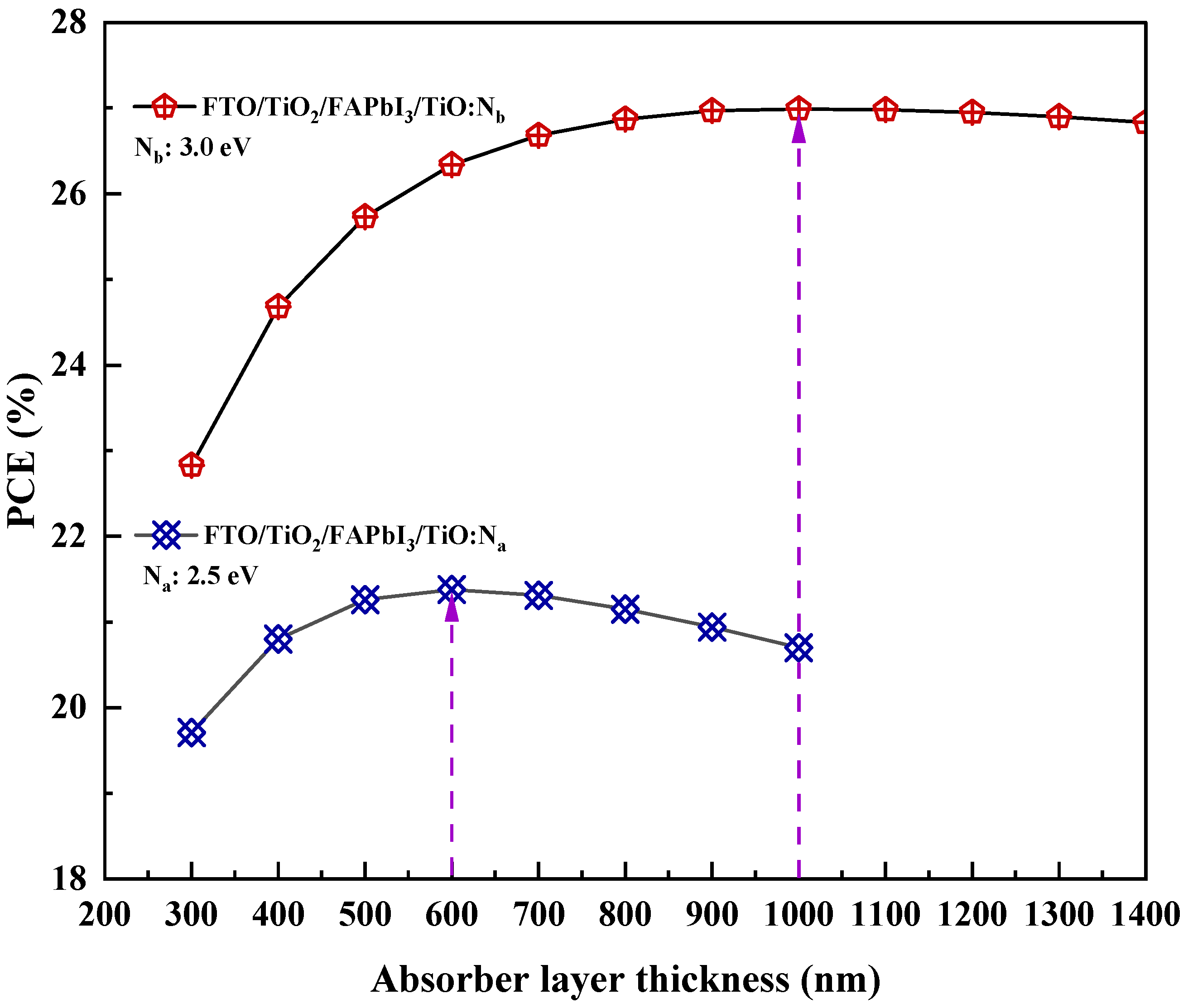
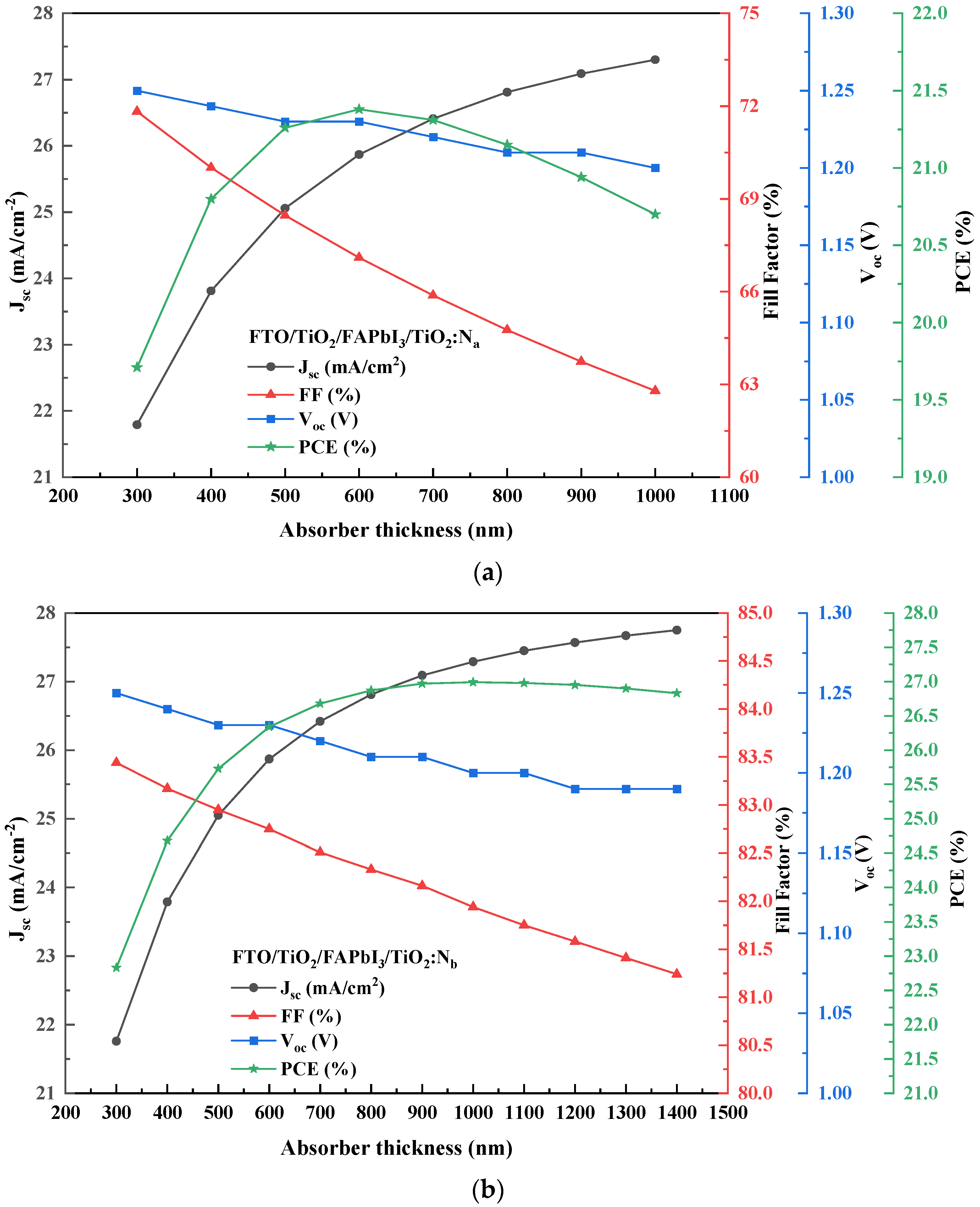
3.1. Effect of Perovskite Absorber Layer Thickness

In this section, a numerical analysis is carried out to investigate the performance output for the designed recipes when the perovskite absorber layer thickness is varied. The PCE is one of the vital factors that is expected to invariably respond to the degree of change in absorber layer thickness. Hence, this attempt would project the optimum and maximum thickness of the absorber layer to yield better output.
Conceptually, the increase in the absorber layer thickness influences the performance parameters of a PSC. With the increase in thickness, the short circuit current (Jsc, mA/cm2) tends to increase since it is attributed to more electron-hole pairs in the absorber layer, whereas the open circuit voltage (Voc, V) decreases due to the increment in the dark saturation current that increases the recombination of charge carriers. Seemingly, the fill factor (FF, %) holds an inversely proportional relationship with an increase in thickness due to the increase in series resistance and internal power dissipation. Additionally, the increase in Jsc and a drop in FF would reflect in the increase of device performance due to the balanced charge transport [5]. Lastly, the power conversion efficiency (PCE, %) tends to increase with thickness but decreases beyond a saturation level (maximum diffusion length). Beyond the saturation point, the fill factor is reported to drop due sheet resistance of the active layer, which is a material perspective phenomenon.
These numerical simulations reveal that the photovoltaic parameters report a change when the layer thickness varies. The primary electrical parameters from Table 3 are considered while the thickness is varied proportionally from 300 nm until the saturation level and maximum allowable thickness is observed. The simulation results show that both recipes’ performance profile has a divergent pattern. The point of convergence for the FTO/FAPbI3/TiO2:Na recipe with 2.5 eV HTL bandgap is below 1.1 V. The FTO/FAPbI3/TiO2:Nb recipe with 3.0 eV HTL bandgap reported the convergence point at 1.2 V, thereby depicting the influence of the HTL bandgap on the cell performance.
Figure 3a,b illustrate the J-V characteristic curve for both recipes based on different HTL bandgaps. It shows that the influence of perovskite absorber layer thickness gradient (∆t) on the performance output is apparent. For both recipes, the absorber layer thickness had a high initial power output that was observed to reduce gradually as the voltage and current increased. As ∆t increased, the PCE (%) was observed to show an incremental pattern. The increase in absorber thickness will enhance electron/hole pair generation and electron mobility. Indeed, the peak of the absorber thickness corresponding to the saturation point is 600 nm FTO/FAPbI3/TiO2:Na recipe and 1000 nm for the FTO/FAPbI3/TiO2:Nb recipe, combinedly depicted in Figure 4, respectively. The patterns obtained in Figure 4 depict a proportionate behaviour among the power conversion efficiency and absorber layer thickness. The increase in HTL bandgap from 2.5 eV to 3.0 eV has fostered the ability to increase the perovskite absorber layer thickness to 1000 nm in recipe-2 before the saturation point can be observed. This is the point beyond which the thermal recombination happens, and the PCE gradually tends to decline. Increasing the absorber layer thickness to up to 1000 nm can attain a higher PCE of up to 26.99% for the corresponding recipe. The performance characteristic attained due to the gradient in ∆t is tabulated in Table 5 and the relation between Jsc, Voc, FF and PCE are illustrated in Figure 5a,b. Therefore, this simulation identifies the peak threshold absorber layer thickness for the FAPbI3 recipes that employ TiO2:N as the HTL and TiO2 as the ETL, respectively.

3.2. Effect of Defect Density in the Perovskite Absorber Layer

The quality and structure of the PSC absorber layer play a significant role in delivering an efficient power output. The defect density (Nt) of the absorber layer influences the performance parameters as the film quality deteriorates. This phenomenon causes a density trap and rise in the recombination of charge carriers, which reflects on the cell output [65]. Madan et al. [66] described that the performance of the PSC is directly influenced by the defect densities on both the perovskite/ETL and the perovskite/HTL. The effect is more intense when light is illuminated from the ETL side due to the high rate of photons being absorbed near the perovskite/ETL interface. This research investigates and reports the impact of defect density from the perovskite/ETL side as the illumination is projected from the ETL side. Hence, this simulation studies the performance of the proposed perovskite recipes with a gradient in defect density (∆Nt) from 1 × 10¹³ to 1 × 1016 cm−3 for the lowest ∆t of 300 nm and the saturation peak ∆t value of 600 nm for recipe-1 and 1000 nm for recipe-2. The J-V characteristics for both recipes are reported in Figure 6a,b. Furthermore, the simulation results notify a consequent drop in the performance output parameters, as reported in Table 6. The simulation results for both recipes infer the impact of the ∆Nt on the PCE (%). With the increase in defect density by 1 × 101 cm−3, the Jsc, FF (%), and Voc were observed to reduce logarithmically, resulting in a drop in the PCE (%) in both the recipes. However, it is observed that the increase in defect density has a lesser influence on the Jsc, but the Voc was observed to respond in proportional change. The FF (%) in recipe-1 was noted to drop drastically with the increased defect density for both the ∆t gradients. Interestingly, though the defect density in recipe-2 increased to 1 × 1016 cm−3, the FF (%) for both the ∆t gradients was attributed to being 54.16% and 44.63%, resulting in the PCE of 11% and 9.17%, which is nearly 1.7 times the PCE attained in recipe-1, respectively. Additionally, it is identified that a reasonable PCE (%) of nearly 16% is attained even if the defect density is increased to 1 × 1015 cm−3 in recipe-2. This output infers the role of the HTL bandgap that increased from 2.5 eV to 3.0 eV in the proposed recipes.

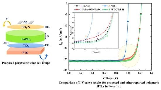
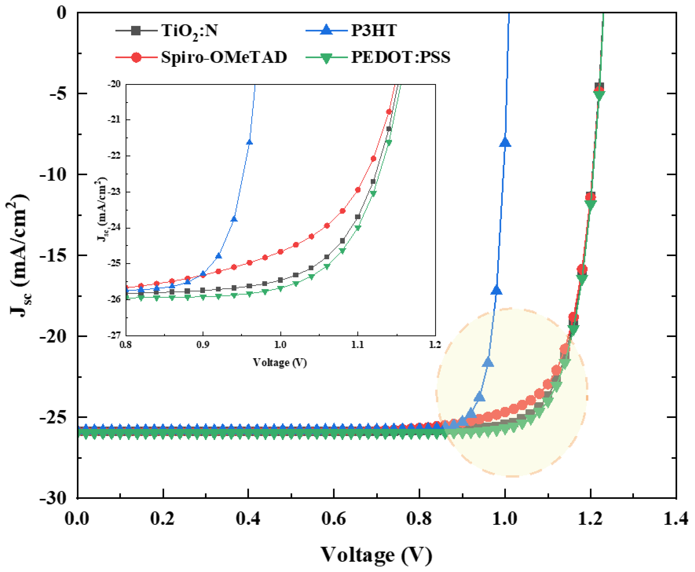
3.3. Comparison of Different Polymeric HTLs Used in an FA-Based PSC Recipe

From the previous sessions, it is evident that the HTL derived from TiO2:N has the potential to deliver adequate electrical performance. Nitrogen doping on c-TiO2 corresponds to developing different bandgaps, which play a functional role in the cell performance. The literature reports (Table 2) that polymeric HTLs such as Spiro-OMeTAD, P3HT, and PEDOT: PSS are most used and viable to feed the role of charge transport mediums in an FA-based cell structure. However, the intrinsic instability, high cost [18,19,67], and multi-step synthesis of these polymeric layers still creates a vacuum for alternative HTLs to be developed.
From the gist of the previous analysis, this further session studies and numerically compares the cell performance output between TiO2:N and polymeric HTLs. The electrical parameters from Table 3 are considered, focusing on attaining a better result with the PSC absorber layer thickness of 600 nm and higher TiO2:N bandgap of 3.0 eV. The polymeric layers’ parameters are considered from the literature in Table 2, which collectively reported simulation and experimental results. Table 7 tabulates the simulative electrical parameters pertaining to this analysis. The J-V curve obtained from numerical simulation is pictured in Figure 7, while the corresponding output performance parameters are tabulated in Table 8.
The performance parameters and the J-V patterns explain the positive potential that is attainable with TiO2:N when used as an HTL in an FTO/TiO2/FAPbI3/HTL/Ag recipe. The magnified view in Figure 7 reports the drift in the short circuit current for the respective HTLs. TiO2:N resulted in a PCE rise of 1.03% and 1.15% over Spiro-OMeTAD and P3HT. It reported a similar trend with 0.9% less PCE against PEDOT: PSS. The Jsc for these recipes was observed to be similar with minor variation, whereas the fill factor was seen to modulate, reflected in the final PCE.

4. Conclusions

In this present study, a formamidinium lead iodide (FAPbI3) perovskite solar cell was optimized with a novel low-cost HTL in the form of nitrogen-doped titanium dioxide (TiO2:N). The performance output influenced by two different HTL bandgaps (2.5 eV and 3.0 eV) was investigated and significantly compared through SCAPS simulation. In addition, the effect of modulation in the absorber layer thickness (∆t) and defect density (∆Nt) was studied, with optimum results reported. The increase in perovskite absorber thickness and increase in HTL bandgap has witnessed a rise in the PCE (%), reaching nearly 26.99%, an exceptional output for a low-cost FAPbI3 solar cell. Though the defect density in the absorber layer increased, the recipe with a high HTL bandgap achieved a reasonable bandgap of 16.59%. Lastly, the behaviour of this HTL was compared with three other polymeric mediums on a standard FA recipe. The simulation results denote a PCE of 26.34%, which is compatibly higher than Spiro-OMeTAD and P3HT. However, the practical feasibility of TiO2:N as a low-cost and stable HTL is undetermined until experimentation is performed, which is considered the future work in this research. Based on simulations, these results conclude that TiO2:N is a suitable HTL that could attain a PCE (%) equivalent to organic and inorganic HTLs. Additionally, with the rendering optical properties in N-doped TiO2, these recipes could aid in developing semi-transparent perovskite cells suited for various applications. Based on the insights gained from this research, this work provides preliminary ways to lower the cost of an FA-based perovskite structure that can be developed soon. Finally, by considering the approaches in Table 2, the viability of different techniques is feasible to confront the phase stability of the α-FAPbI3 structure.

Author Contributions

Conceptualization: N.R.P., Y.R.S. and K.V.; Methodology: N.R.P. and Y.R.S.; Validation: N.R.P., Y.R.S., R.J. and K.V.; Investigation: R.J. and K.V.; Writing—Original draft preparation: N.R.P.; Review and Editing: N.R.P., Y.R.S., R.J. and K.V.; Supervision: Y.R.S. All authors have read and agreed to the published version of the manuscript.

Funding

This research received no external funding.

Institutional Review Board Statement

Not applicable.

Informed Consent Statement

Not applicable.

Data Availability Statement

Not applicable.

Acknowledgments

The authors thank Marc Burgelman, ELSI, University of Gent, Belgium, for providing the SCAPS 3.8 version simulation software used in this numerical study. In addition, K.V. wishes to thank the DST-SERB (project ID: EEQ/2020/000319) Govt. of India for financial support of the work. R.J. acknowledges Universiti Malaysia Pahang for the grant RDU203301.

Conflicts of Interest

The authors declare that there is no conflict of interest in this work.

References

  1. Xue, L.; Liu, X.; Wang, Q.; Yang, M.; Du, S.; Yang, C.; Tong, J.; Xia, Y.; Li, J. Improved Performance of Organic Solar Cells by Utilizing Green Non-Halogen Additive to Modulate Active-Layer Morphology. Energy Technol. 2022, 10, 2200504. [Google Scholar] [CrossRef]
  2. Rao, V.T.; Sekhar, Y.R. Comparative analysis on embodied energy and CO2 emissions for stand-alone crystalline silicon photovoltaic thermal (PVT) systems for tropical climatic regions of India. Sustain. Cities Soc. 2022, 78, 103650. [Google Scholar] [CrossRef]
  3. Yang, D.; Zhang, X.; Hou, Y.; Wang, K.; Ye, T.; Yoon, J.; Wu, C.; Sanghadasa, M.; Liu, S.; Priya, S. 28.3%-efficiency perovskite/silicon tandem solar cell by optimal transparent electrode for high efficient semitransparent top cell. Nano Energy 2021, 84, 105934. [Google Scholar] [CrossRef]
  4. Rao, V.T.; Sekhar, Y.R. Hybrid Photovoltaic/Thermal (PVT) Collector Systems with Different Absorber Configurations for Thermal Management—A Review. Energy Environ. 2021, 0958305X211065575. [Google Scholar] [CrossRef]
  5. Ren, Y.; Liu, X.; Li, H.; Qin, J.; Du, S.; Lu, X.; Tong, J.; Yang, C.; Li, J. Utilizing non-conjugated small-molecular tetrasodium iminodisuccinateas electron transport layer enabled improving efficiency of organic solar cells. Opt. Mater. 2022, 129, 112520. [Google Scholar] [CrossRef]
  6. Ehrler, B.; Alarcón-Lladó, E.; Tabernig, S.W.; Veeken, T.; Garnett, E.C.; Polman, A. Photovoltaics Reaching for the Shockley–Queisser Limit. ACS Energy Lett. 2020, 5, 3029–3033. [Google Scholar] [CrossRef]
  7. Nalianya, M.A.; Awino, C.; Barasa, H.; Odari, V.; Gaitho, F.; Omogo, B.; Mageto, M. Numerical study of lead free CsSn0.5Ge0.5I3 perovskite solar cell by SCAPS-1D. Optik 2021, 248, 168060. [Google Scholar] [CrossRef]
  8. Ahmed, S.; Jannat, F.; Khan, A.K.; Alim, M.A. Numerical development of eco-friendly Cs2TiBr6 based perovskite solar cell with all-inorganic charge transport materials via SCAPS-1D. Optik 2020, 225, 165765. [Google Scholar] [CrossRef]
  9. Liu, G.; Liu, Z.; Wang, L.; Zhang, K.; Xie, X. A combined chrome oxide and titanium oxide based electron-transport layer for high-performance perovskite solar cells. Chem. Phys. Lett. 2021, 771, 138496. [Google Scholar] [CrossRef]
  10. NREL. Best Research-Cell Efficiency Chart. 2022. Available online: https://www.nrel.gov/pv/cell-efficiency.html (accessed on 5 October 2022).
  11. Lin, L.; Jiang, L.; Li, P.; Fan, B.; Qiu, Y.; Yan, F. Simulation of optimum band structure of HTM-free perovskite solar cells based on ZnO electron transporting layer. Mater. Sci. Semicond. Process. 2018, 90, 1–6. [Google Scholar] [CrossRef]
  12. Chen, C.; Zheng, S.; Song, H. Photon management to reduce energy loss in perovskite solar cells. Chem. Soc. Rev. 2021, 50, 7250–7329. [Google Scholar] [CrossRef] [PubMed]
  13. Chiara, R.; Morana, M.; Malavasi, L. Germanium-Based Halide Perovskites: Materials, Properties, and Applications. ChemPlusChem 2021, 86, 879–888. [Google Scholar] [CrossRef] [PubMed]
  14. Correa-Baena, J.-P.; Nienhaus, L.; Kurchin, R.C.; Shin, S.S.; Wieghold, S.; Hartono, N.T.P.; Layurova, M.; Klein, N.D.; Poindexter, J.R.; Polizzotti, A.; et al. A-Site Cation in Inorganic A3Sb2I9 Perovskite Influences Structural Dimensionality, Exciton Binding Energy, and Solar Cell Performance. Chem. Mater. 2018, 30, 3734–3742. [Google Scholar] [CrossRef]
  15. Tai, Q.; Tang, K.-C.; Yan, F. Recent progress of inorganic perovskite solar cells. Energy Environ. Sci. 2019, 12, 2375–2405. [Google Scholar] [CrossRef]
  16. Nam, J.K.; Chai, S.U.; Cha, W.; Choi, Y.J.; Kim, W.; Jung, M.S.; Kwon, J.; Kim, D.; Park, J.H. Potassium Incorporation for Enhanced Performance and Stability of Fully Inorganic Cesium Lead Halide Perovskite Solar Cells. Nano Lett. 2017, 17, 2028–2033. [Google Scholar] [CrossRef] [PubMed]
  17. Gkini, K.E.; Antoniadou, M.; Balis, N.; Kaltzoglou, A.; Kontos, A.G.; Falaras, P. Mixing cations and halide anions in perovskite solar cells. Mater. Today Proc. 2019, 19, 73–78. [Google Scholar] [CrossRef]
  18. Shao, S.; Loi, M.A. The Role of the Interfaces in Perovskite Solar Cells. Adv. Mater. Interfaces 2019, 7, 1901469. [Google Scholar] [CrossRef] [Green Version]
  19. Zhou, D.; Zhou, T.; Tian, Y.; Zhu, X.; Tu, Y. Perovskite-Based Solar Cells: Materials, Methods, and Future Perspectives. J. Nanomater. 2018, 2018, 8148072. [Google Scholar] [CrossRef]
  20. Nhari, L.M.; El-Shishtawy, R.M.; Asiri, A.M. Recent progress in organic hole transport materials for energy applications. Dye. Pigment. 2021, 193, 109465. [Google Scholar] [CrossRef]
  21. Wang, Q.; Lin, Z.; Su, J.; Hu, Z.; Chang, J.; Hao, Y. Recent progress of inorganic hole transport materials for efficient and stable perovskite solar cells. Nano Sel. 2021, 2, 1055–1080. [Google Scholar] [CrossRef]
  22. Li, S.; Cao, Y.-L.; Li, W.-H.; Bo, Z.-S. A brief review of hole transporting materials commonly used in perovskite solar cells. Rare Met. 2021, 40, 2712–2729. [Google Scholar] [CrossRef]
  23. Kim, J.; Kim, K.S.; Myung, C.W. Efficient electron extraction of SnO2 electron transport layer for lead halide perovskite solar cell. NPJ Comput. Mater. 2020, 6, 100. [Google Scholar] [CrossRef]
  24. Bendib, T.; Bencherif, H.; Abdi, M.; Meddour, F.; Dehimi, L.; Chahdi, M. Combined optical-electrical modeling of perovskite solar cell with an optimized design. Opt. Mater. 2020, 109, 110259. [Google Scholar] [CrossRef]
  25. Hima, A.; Lakhdar, N. Enhancement of efficiency and stability of CH3NH3GeI3 solar cells with CuSbS2. Opt. Mater. 2019, 99, 109607. [Google Scholar] [CrossRef]
  26. Bhavsar, K.; Lapsiwala, P. Numerical simulation of perovskite solar cell with different material as electron transport layer using SCAPS-1D Software. Semicond. Phys. Quantum Electron. Optoelectron. 2021, 24, 341–347. [Google Scholar] [CrossRef]
  27. Kim, T.; Lim, J.; Song, S. Recent Progress and Challenges of Electron Transport Layers in Organic–Inorganic Perovskite Solar Cells. Energies 2020, 13, 5572. [Google Scholar] [CrossRef]
  28. Assi, A.A.; Saleh, W.R.; Mohajerani, E. Investigate of TiO2 and SnO2 as electron transport layer for perovskite solar cells. AIP Conf. Proc. 2020, 2290, 050039. [Google Scholar] [CrossRef]
  29. Asahi, R.; Morikawa, T.; Irie, H.; Ohwaki, T. Nitrogen-Doped Titanium Dioxide as Visible-Light-Sensitive Photocatalyst: Designs, Developments, and Prospects. Chem. Rev. 2014, 114, 9824–9852. [Google Scholar] [CrossRef]
  30. Zafar, M.; Yun, J.-Y.; Kim, D.-H. Performance of inverted organic photovoltaic cells with nitrogen doped TiO2 films by atomic layer deposition. Korean J. Chem. Eng. 2018, 35, 567–573. [Google Scholar] [CrossRef]
  31. Mahmood, K.; Sarwar, S.; Mehran, M.T. Current status of electron transport layers in perovskite solar cells: Materials and properties. RSC Adv. 2017, 7, 17044–17062. [Google Scholar] [CrossRef]
  32. Ansari, S.A.; Khan, M.M.; Ansari, M.O.; Cho, M.H. Nitrogen-doped titanium dioxide (N-doped TiO2) for visible light photocatalysis. New J. Chem. 2016, 40, 3000–3009. [Google Scholar] [CrossRef]
  33. Kim, T.H.; Go, G.-M.; Cho, H.-B.; Song, Y.; Lee, C.-G.; Choa, Y.-H. A novel synthetic method for N doped TiO2 nanoparticles through plasma-assisted electrolysis and photocatalytic activity in the visible region. Front. Chem. 2018, 6, 458. [Google Scholar] [CrossRef] [PubMed] [Green Version]
  34. Panepinto, A.; Dervaux, J.; Cormier, P.A.; Boujtita, M.; Odobel, F.; Snyders, R. Synthesis of p-type N-doped TiO2 thin films by co-reactive magnetron sputtering. Plasma Process. Polym. 2020, 17, 1900203. [Google Scholar] [CrossRef]
  35. Santos, I.M.D.L.; Cortina-Marrero, H.J.; Ruíz-Sánchez, M.; Hechavarría-Difur, L.; Sánchez-Rodríguez, F.; Courel, M.; Hu, H. Optimization of CH3NH3PbI3 perovskite solar cells: A theoretical and experimental study. Sol. Energy 2020, 199, 198–205. [Google Scholar] [CrossRef]
  36. Mamta; Maurya, K.; Singh, V. Sb2Se3 versus Sb2S3 solar cell: A numerical simulation. Sol. Energy 2021, 228, 540–549. [Google Scholar] [CrossRef]
  37. Sebastian, V.; Kurian, J. Simulation and optimization studies on CsPbI3 based inorganic perovskite solar cells. Sol. Energy 2021, 221, 99–108. [Google Scholar] [CrossRef]
  38. Vasu, K.; Sreedhara, M.B.; Ghatak, J.; Rao, C.N.R. Atomic Layer Deposition of p-Type Epitaxial Thin Films of Undoped and N-Doped Anatase TiO2. ACS Appl. Mater. Interfaces 2016, 8, 7897–7901. [Google Scholar] [CrossRef]
  39. Lee, M.D.; Lee, G.J.; Nam, I.; Abbas, M.A.; Bang, J.H. Exploring the Effect of Cation Vacancies in TiO2: Lithiation Behavior of n-Type and p-Type TiO2. ACS Appl. Mater. Interfaces 2022, 14, 6560–6569. [Google Scholar] [CrossRef]
  40. Vasilopoulou, M.; Kelaidis, N.; Polydorou, E.; Soultati, A.; Davazoglou, D.; Argitis, P.; Papadimitropoulos, G.; Tsikritzis, D.; Kennou, S.; Auras, F.; et al. Hydrogen and nitrogen codoping of anatase TiO2 for efficiency enhancement in organic solar cells. Sci. Rep. 2017, 7, 17839. [Google Scholar] [CrossRef] [Green Version]
  41. Anitha, V.C.; Banerjee, A.N.; Joo, S.W. Recent developments in TiO2 as n- and p-type transparent semiconductors: Synthesis, modification, properties, and energy-related applications. J. Mater. Sci. 2015, 50, 7495–7536. [Google Scholar] [CrossRef]
  42. Bakar, S.A.; Ribeiro, C. Nitrogen-doped titanium dioxide: An overview of material design and dimensionality effect over modern applications. J. Photochem. Photobiol. C Photochem. Rev. 2016, 27, 1–29. [Google Scholar] [CrossRef]
  43. Fu, C.; Gu, Z.; Tang, Y.; Xiao, Q.; Zhang, S.; Zhang, Y.; Song, Y. From Structural Design to Functional Construction: Amine Molecules in High-Performance Formamidinium-Based Perovskite Solar Cells. Angew. Chem. 2022, 134, e202117067. [Google Scholar] [CrossRef]
  44. Zheng, Z.; Wang, S.; Hu, Y.; Rong, Y.; Mei, A.; Han, H. Development of formamidinium lead iodide-based perovskite solar cells: Efficiency and stability. Chem. Sci. 2021, 13, 2167–2183. [Google Scholar] [CrossRef] [PubMed]
  45. Dong, X.; Chao, L.; Niu, T.; Li, Y.; Guo, P.; Hui, W.; Song, L.; Wu, Z.; Chen, Y. Phase-Pure Engineering for Efficient and Stable Formamidinium-Based Perovskite Solar Cells. Sol. RRL 2022, 6, 2200060. [Google Scholar] [CrossRef]
  46. Wang, Y.; Wang, X.; Wang, C.; Cheng, R.; Zhao, L.; Wang, X.; Zhang, X.; Shang, J.; Zhang, H.; Zhao, L.; et al. Defect suppression and energy level alignment in formamidinium-based perovskite solar cells. J. Energy Chem. 2021, 67, 65–72. [Google Scholar] [CrossRef]
  47. Kundu, S.; Zhang, D.; Askar, A.M.; Moloney, E.G.; Adachi, M.M.; Nadeem, A.; Moradi, S.; Yeddu, V.; Abdelhady, A.L.; Voznyy, O.; et al. Bismuth Stabilizes the α-Phase of Formamidinium Lead Iodide Perovskite Single Crystals. ACS Mater. Lett. 2022, 4, 707–712. [Google Scholar] [CrossRef]
  48. Bu, T.; Ono, L.K.; Li, J.; Su, J.; Tong, G.; Zhang, W.; Liu, Y.; Zhang, J.; Chang, J.; Kazaoui, S.; et al. Modulating crystal growth of formamidinium–caesium perovskites for over 200 cm2 photovoltaic sub-modules. Nat. Energy 2022, 7, 528–536. [Google Scholar] [CrossRef]
  49. Liu, S.; Chen, R.; Tian, X.; Yang, Z.; Zhou, J.; Ren, F.; Zhang, S.; Zhang, Y.; Guo, M.; Shen, Y.; et al. Boost the efficiency of nickel oxide-based formamidinium-cesium perovskite solar cells to 21% by using coumarin 343 dye as defect passivator. Nano Energy 2022, 94, 106935. [Google Scholar] [CrossRef]
  50. Li, Y.; Chen, Z.; Yu, B.; Tan, S.; Cui, Y.; Wu, H.; Luo, Y.; Shi, J.; Li, D.; Meng, Q. Efficient, stable formamidinium-cesium perovskite solar cells and minimodules enabled by crystallization regulation. Joule 2022, 6, 676–689. [Google Scholar] [CrossRef]
  51. Vishnuwaran, M.; Ramachandran, K.; Anand, D.; Ragavendran, V. Using low-cost materials for highly efficient eco-friendly formamidinium tin iodide based solar cell with copper oxide as hole transport material and titanium oxide as electron transport material with different metal contacts. Ceram. Int. 2022, 48, 29314–29321. [Google Scholar] [CrossRef]
  52. Niloy, A.B.; Al Razy, M.; Ahmed, S.; Jannat, F.; Alim, M.A. Performance investigation of cesium formamidinium lead mixed halide (FA0.83Cs0.17PbI3−xBrx) for different iodine and bromine ratios. Micro Nanostructures 2022, 168, 207305. [Google Scholar] [CrossRef]
  53. Sabbah, H.; Arayro, J.; Mezher, R. Numerical Simulation and Optimization of Highly Stable and Efficient Lead-Free Perovskite FA1−xCsxSnI3−x Based Solar Cells Using SCAPS. Materials 2022, 15, 4761. [Google Scholar] [CrossRef] [PubMed]
  54. Vishnuwaran, M.; Ramachandran, K. Novel Approach on Formamidinium Tin Iodide-Based Provskite Solar Cell for the Best Replacement Materials of Hole Transport Layer and Electron Transport Layer by Using Solar Cell Capacitance Simulation; Research Square: Durham, NC, USA, 2022. [Google Scholar] [CrossRef]
  55. Teimouri, R.; Mehrvarz, S.; Ebrahimi, A.; Kolahdouz, M.; Darab, M. Performance of planar perovskite solar cells based on formamidinium cations: Simulation and fabrication. Int. J. Energy Res. 2022. [Google Scholar] [CrossRef]
  56. Jannat, F.; Ahmed, S.; Alim, M.A. Performance analysis of cesium formamidinium lead mixed halide based perovskite solar cell with MoOx as hole transport material via SCAPS-1D. Optik 2020, 228, 166202. [Google Scholar] [CrossRef]
  57. Stanić, D.; Kojić, V.; Čižmar, T.; Juraić, K.; Bagladi, L.; Mangalam, J.; Rath, T.; Gajović, A. Simulating the Performance of a Formamidinium Based Mixed Cation Lead Halide Perovskite Solar Cell. Materials 2021, 14, 6341. [Google Scholar] [CrossRef]
  58. Alipour, H.; Ghadimi, A. Optimization of lead-free perovskite solar cells in normal-structure with WO3 and water-free PEDOT: PSS composite for hole transport layer by SCAPS-1D simulation. Opt. Mater. 2021, 120, 111432. [Google Scholar] [CrossRef]
  59. Tara, A.; Bharti, V.; Sharma, S.; Gupta, R. Device simulation of FASnI3 based perovskite solar cell with Zn (O0.3, S0.7) as electron transport layer using SCAPS-1D. Opt. Mater. 2021, 119, 111362. [Google Scholar] [CrossRef]
  60. Patil, S.V.; Dave, S.; Bhargava, K. Comparative Analysis of MAPbI3 and FAPbI3 based Perovskite Solar Cells: A Numerical Evaluation. In Proceedings of the 28th National Conference on Condensed Matter Physics, NIT Silchar, India, 11–13 December 2021; Springer: Singapore, 2021; pp. 177–185. [Google Scholar] [CrossRef]
  61. Kanoun, M.B.; Kanoun, A.A.; Merad, A.E.; Goumri-Said, S. Device design optimization with interface engineering for highly efficient mixed cations and halides perovskite solar cells. Results Phys. 2021, 20, 103707. [Google Scholar] [CrossRef]
  62. Bhardwaj, K.S.; Rai, S.; Sadanand; Lohia, P.; Dwivedi, D.K. Investigating the performance of mixed cation mixed halide-based perovskite solar cells using various hole-transport materials by numerical simulation. Opt. Quantum Electron. 2021, 53, 602. [Google Scholar] [CrossRef]
  63. Kumar, M.; Raj, A.; Kumar, A.; Anshul, A. An optimized lead-free formamidinium Sn-based perovskite solar cell design for high power conversion efficiency by SCAPS simulation. Opt. Mater. 2020, 108, 110213. [Google Scholar] [CrossRef]
  64. Karthick, S.; Velumani, S.; Bouclé, J. Experimental and SCAPS simulated formamidinium perovskite solar cells: A comparison of device performance. Sol. Energy 2020, 205, 349–357. [Google Scholar] [CrossRef]
  65. Hussain, S.S.; Riaz, S.; Nowsherwan, G.A.; Jahangir, K.; Raza, A.; Iqbal, M.J.; Sadiq, I.; Naseem, S. Numerical Modeling and Optimization of Lead-Free Hybrid Double Perovskite Solar Cell by Using SCAPS-1D. J. Renew. Energy 2021, 2021, 6668687. [Google Scholar] [CrossRef]
  66. Madan, J.; Singh, K.; Pandey, R. Comprehensive device simulation of 23.36% efficient two-terminal perovskite-PbS CQD tandem solar cell for low-cost applications. Sci. Rep. 2021, 11, 19829. [Google Scholar] [CrossRef]
  67. Kim, G.; Choi, H.; Kim, M.; Lee, J.; Son, S.Y.; Park, T. Hole Transport Materials in Conventional Structural (n–i–p) Perovskite Solar Cells: From Past to the Future. Adv. Energy Mater. 2020, 10, 1903403. [Google Scholar] [CrossRef]
  68. Rono, N.; Merad, A.E.; Kibet, J.K.; Martincigh, B.S.; Nyamori, V.O. Optimization of Hole Transport Layer Materials for a Lead-Free Perovskite Solar Cell Based on Formamidinium Tin Iodide. Energy Technol. 2021, 9, 2100859. [Google Scholar] [CrossRef]
Figure 1. (a) Structure of the PSC with TiO2 as ETL and TiO2:N as HTL; (b) energy band diagram of the PSC layers with FAPbI3 absorber layer and different bandgap HTLs.
Molecules 27 07927 g001
Figure 2. (a) Simulated J-V characteristics for the two PSC recipes. (b) Quantum efficiency spectrum of the simulated PSC recipes.
Molecules 27 07927 g002
Figure 3. (a) (i) J-V characteristic curve for the FTO/FAPbI3/TiO2:Na recipe with ∆t; (ii) a magnified view of the convergence point from the applied voltage range 0.8–1.1 V. (b) (i) J-V characteristic curve for the FTO/FAPbI3/TiO2:Nb recipe with ∆t; (ii) a magnified view of the convergence point in the applied voltage range 1.08–1.18 V.
Molecules 27 07927 g003
Figure 4. Spectrum of the maximum allowable absorber layer thickness for both recipes.
Molecules 27 07927 g004
Figure 5. (a) Performance parameter curves for the FTO/FAPbI3/TiO2:Na recipe. (b) Performanc parameter curves for the FTO/FAPbI3/TiO2:Nb recipe.
Molecules 27 07927 g005
Figure 6. (a) J-V curve for the FTO/FAPbI3/TiO2:Na recipe with ∆Nt. (b) J-V curve for the FTO/FAPbI3/TiO2:Nb recipe with ∆Nt.
Molecules 27 07927 g006
Figure 7. J-V characteristic curve for the HTL comparative analysis with a magnified view that depicts the drift patterns between 0.8–1.2 V.
Molecules 27 07927 g007
Table 1. Recent research that reports the techniques to stabilize the pure α-FAPbI3 state.
S. No.YearAuthor [Reference]RecipeRemarks
12022Wang et al. [46]SnO2/FAPSC/Spiro-OMeTAD4-fluorophenylmethylammonium iodide (F-PMAI) was used to modulate surface structure and energy level alignment.
22022Kundu et al. [47]FAPbI3 crystalsThe α-FAPbI3 single crystals are stabilized through Pb-site doping with a heterovalent metal–bismuth (Bi). The optimum concentration of Bi extends the phase change by four orders of magnitude.
32022Bu et al. [48](FA-Cs) lead halideControlled the formation of intermediate phases during the growth of formamidinium–caesium lead triiodide perovskite films by using methylammonium chloride additives in the co-solvent system of N-methyl-2-pyrrolidone/N, N-dimethylformamide.
42022Liu et al. [49]FA-Cs + NiOx (HTL)A molecular additive—the organic dye coumarin 343—was used to reduce Voc loss and improve efficiency.
52022Li et al. [50](FA-Cs) lead halideAdditives reduced crystallization and defects of the FA-Cs perovskite film.
Table 2. Recent simulations that report various organic and inorganic HTLs adopted in an FA-based PSC structure (2022–2021).
S. No.YearAuthorPerovskite Solar Cell Structure (ETL/Absorber/HTL)Performance Factors (Voc (V), Jsc (mA/cm2), FF (%), PCE (%)RemarksReference
12022Vishnuwaran et al.TiO2/FASnI3/CuO2Voc: 0.7921, Jsc: 29.61, FF: 78.14, PCE: 18.10Varied absorber layer thickness—350 nm yielded the best results[51]
22022Niloy et al.SnO2/FA0.83Cs0.17PbI0.5Br2.5/MoOxPCE up to 22.89% for absorber thickness of 169 nmAbsorber layer thickness influences the PCE[52]
32022Sabbah et al.(TiO2, ZnOS)/FA1−xCsxSnI3/CuO2Voc: 0.89, Jsc: 31.4, FF: 78.7, PCE: 22ZnOS exhibited stable behaviour and was better than TiO2[53]
42022VishnuwaranZnOS/FASnI3/CuIVoc: 6.20, Jsc: 30.77, FF: 12.68, PCE: 24.22CuI and ZnOS are considered ideal replacements for Spiro-OMeTAD and TiO2[54]
52022Teimouri et al.Cs0.05 (FAxMA[1−x])0.95Pb(I0.83Br0.17)3Attained a PCE of up to 20.98%Analyzed bandgap ratios between 2.175 eV to 1.5 eV and x factor influenced the power output[55]
62021Jannat et al.SnO2/FA0.83Cs0.17 PbI1.5Br1.5/MoOxVoc: 1.44, Jsc: 17.04, FF: 81.83, PCE: 20.10MoOx exhibited a low valence band offset. HTL and absorber thickness was varied[56]
72021Stanić et al.TiO2/Rb0.05Cs0.1FA0.85PbI3/Spiro-OMeTADVoc: 0.80, Jsc: 20.60, FF: 45.51, PCE: 7.35Absorber layer thickness, defect density concentration, and the influence of the resistivity were analyzed[57]
82021Alipour and GhadimiPC61BM/FASnI3/PEDOT: PSS+WO3Voc: 1.12, Jsc: 24.65, FF: 86.02, PCE: 23.69FA depicted better outputs that MA based structures[58]
92021Tara et al.Zn (O0.3, S0.7)/FASnI3/CuSCNVoc: 1.08, Jsc: 28.12, FF: 84.96, PCE: 25.94Variations in electron affinity, CBO, doping density, and thickness of Zn (O0.3, S0.7) were analyzed[59]
102021Patil et al.ZnO/FAPbI3/Spiro-OMeTADVoc: 0.99, Jsc: 26.75, FF: 79.80, PCE: 21.26FA-based PSC structures have depicted higher efficiency than MA[60]
112021Kanoun et al.TiO2/FAPbI3/PTAA and Cu2OPCE of up to 24% for absorber thickness of 400 nmPTAA and Cu2O as HTLs enhance change carriers[61]
122021Bhardwaj et al.SnO2/FA0.85Cs0.15Pb(I0.85Br0.15)3/Spiro-OMeTAD and Cu2OSpiro-OMeTAD (HTL)—PCE: 15.36% Cuprous oxide (HTL)—PCE: 19.38%CuO2 delivers the highest efficiency when compared to other inorganic HTLs[62]
Table 4. Summarised photovoltaic parameters of the two recipes from SCAPS simulation.
PSC RecipeJsc (mA/cm−2)FF (%)Voc (V)PCE (%)
FTO/TiO2/FAPbI3/TiO2:Na/Ag21.79871.831.2519.71
FTO/TiO2/FAPbI3/TiO2:Nb/Ag21.76083.441.2522.83
Table 5. Performance parameters for both recipes with varied ∆t.
Recipe∆t (nm)Jsc (mA/cm−2)FF (%)Voc (V)PCE (%)
FTO/TiO2/FAPbI3/
TiO2:Na/Ag
30021.7971.831.2519.71
40023.8170.011.2420.80
50025.0668.461.2321.26
600 #25.8767.101.2321.38
70026.4165.881.2221.31
80026.8164.761.2121.15
90027.0963.741.2120.94
100027.3062.791.2020.70
FTO/TiO2/FAPbI3/
TiO2:Nb/Ag
30021.7683.441.2522.83
40023.7983.171.2424.68
50025.0582.951.2325.73
60025.8782.751.2326.34
70026.4282.511.2226.68
80026.8182.331.2126.87
90027.0982.161.2126.97
1000 #27.2981.941.2026.99
110027.4581.751.2026.98
120027.5781.581.1926.95
130027.6781.411.1926.90
140027.7581.241.1926.83
# Saturation point.
Table 6. Performance parameters for proposed recipes with ∆Nt and ∆t.
RecipeAbsorber Layer Thickness (∆t)Defect Density (Nt)Jsc (mA/cm−2)FF (%)Voc (V)PCE (%)
FTO/TiO2/FAPbI3/
TiO2:Na/Ag
300 nm1 × 101321.7971.831.2519.71
1 × 101421.7955.151.1413.92
1 × 101521.7545.681.0510.44
1 × 101621.3133.120.997.06
600 nm #1 × 101325.8767.101.2321.38
1 × 101425.8548.791.1114.08
1 × 101526.6237.121.019.62
1 × 101623.7222.170.934.94
FTO/TiO2/FAPbI3/
TiO2:Nb/Ag
300 nm1 × 101321.7683.441.2522.83
1 × 101421.7581.761.1420.31
1 × 101521.7172.571.0316.33
1 × 101621.3154.160.9511.00
1000 nm #1 × 101327.2981.941.2026.99
1 × 101427.2774.821.0822.22
1 × 101526.9963.020.9716.59
1 × 101624.4544.630.849.17
# Saturation point.
Table 7. Simulation parameters for TiO2:N and Polymeric HTLs.
ParametersSubstrateETLPerovskite Absorber LayerNovel HTLPolymeric HTLs
FTOTiO2FAPbI3TiO2:NSpiro-OMeTAD [62]P3HT [68]PEDOT: PSS [58]
Thickness ‘t’ (nm)4005060010020050200
Band gap ‘Eg’ (eV)3.53.21.513.02.881.11.8
Electron affinity ‘χ’ (eV)4442.22.054.63.4
Dielectric Permittivity ‘εr996.63313.618
CB EDOS ‘Nc’ (cm−3)2.2 × 10182.1 × 10181.2 × 10191.3 × 10142.2 × 10183 × 10182.2 × 1018
VB EDOS ‘Nv’ (cm−3)2.2 × 10182.2 × 10171.2 × 10191.3 × 10151.8 × 10192 × 10191.8 × 1019
e thermal velocity (cm·s−1)1 × 1071 × 1071 × 1071 × 1071 × 1071 × 1071 × 107
h+ thermal velocity (cm·s−1)1 × 1071 × 1071 × 1071 × 1071 × 1071 × 1071 × 107
Electron mobility ‘μn’ (cm2/V·s)20202.722 × 10−4254.5 × 10−2
Hole mobility ‘μh’ (cm2/V·s)10101.822 × 10−4254.5 × 10−2
Shallow donor density ‘N.D.’ (cm−3)2 × 10199 × 10161.3 × 10160000
Shallow Acceptor density ‘N.A.’ (cm−3)001.3 × 10161.3 × 10142 × 10193 × 10161 × 1020
Defect density ‘Nt’ (cm−3)1 × 10151 × 10151 × 10131 × 10151 × 10151 × 10131 × 1015
Table 8. Performance parameters attained from the HTL comparative analysis.
PSC RecipeJsc (mA/cm−2)FF (%)Voc (V)PCE (%)
FTO/TiO2/FAPbI3/TiO2:N/Ag25.8782.751.2326.34
FTO/TiO2/FAPbI3/Spiro-OMeTAD/Ag25.8679.831.2325.42
FTO/TiO2/FAPbI3/P3HT/Ag25.8187.621.0122.85
FTO/TiO2/FAPbI3/PEDOT: PSS/Ag25.9583.301.2326.61
Publisher’s Note: MDPI stays neutral with regard to jurisdictional claims in published maps and institutional affiliations.

