
Charge Transfer in Patterned Bilayer Film of Ag/ZnS Composite by Magnetron Control Sputtering

Abstract
:1. Introduction
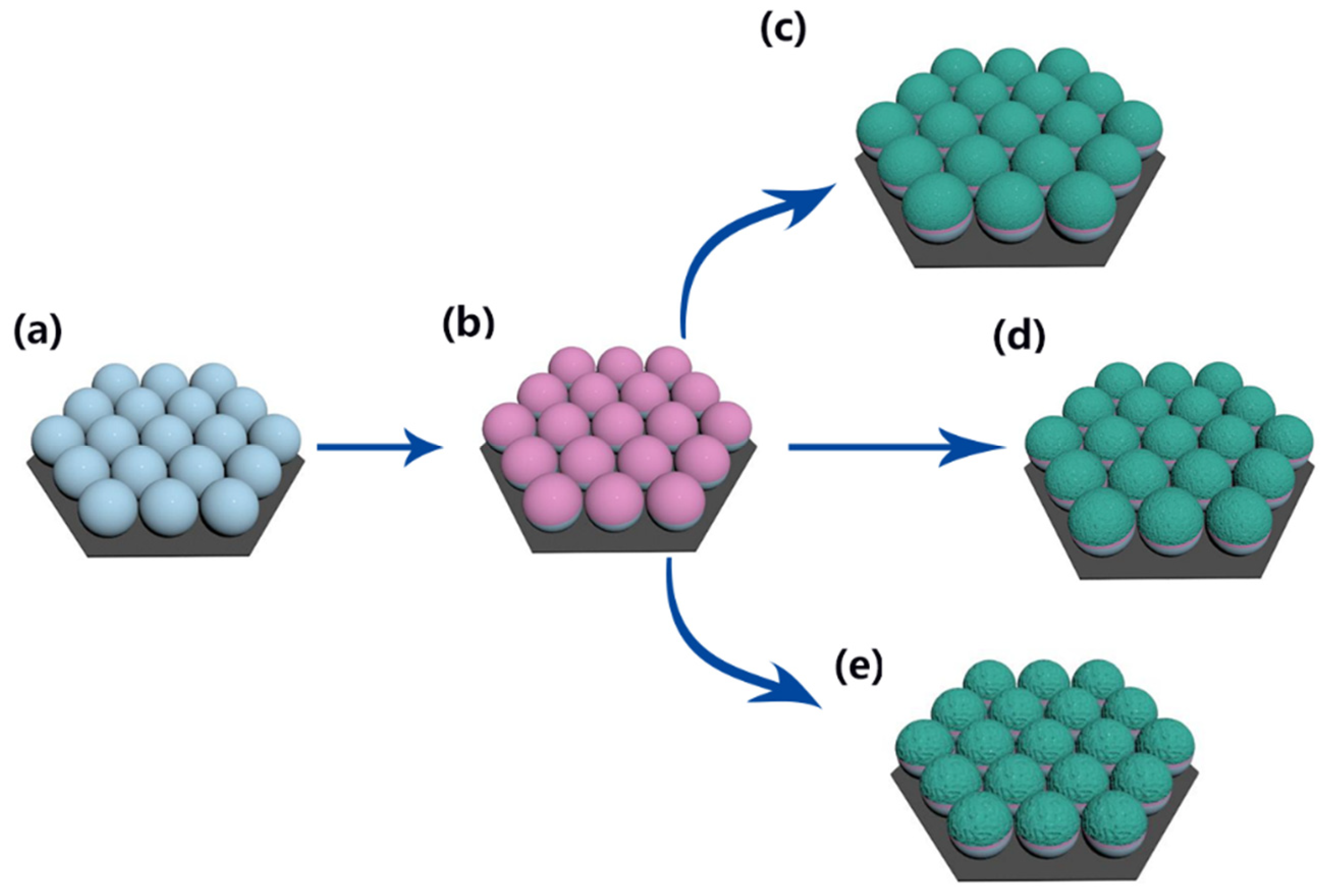
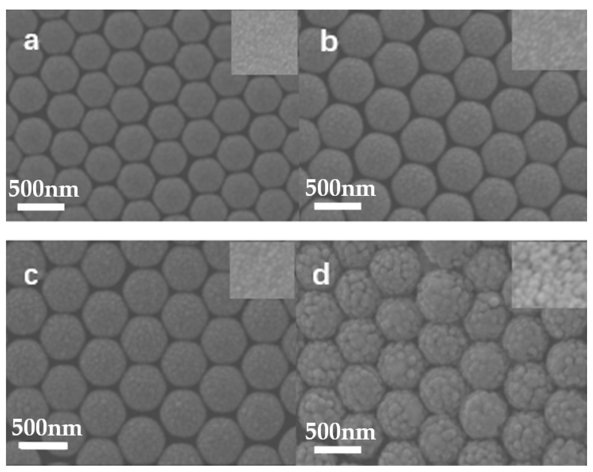
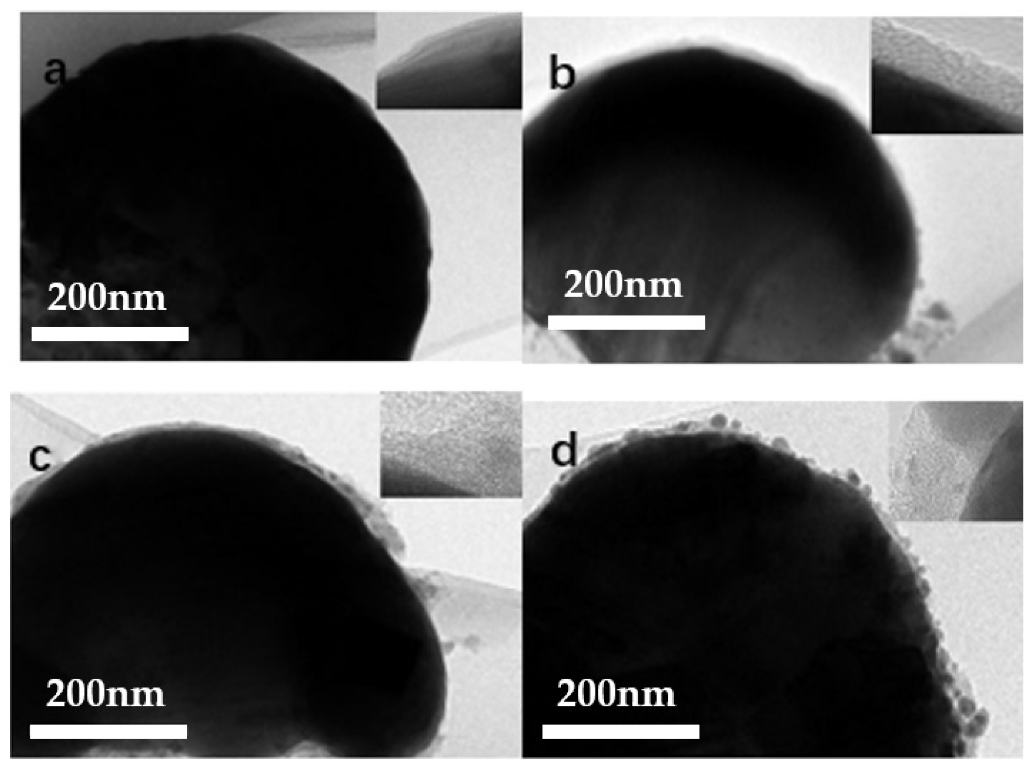
2. Experiments
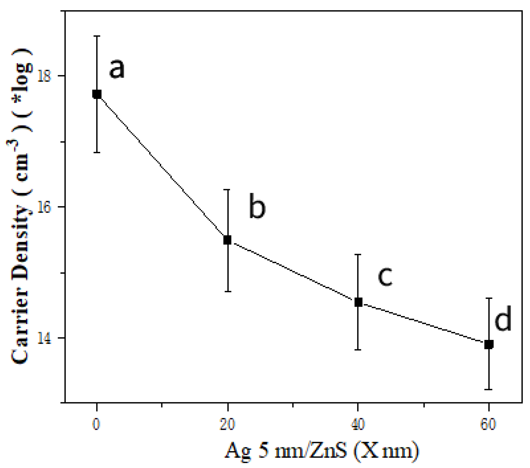
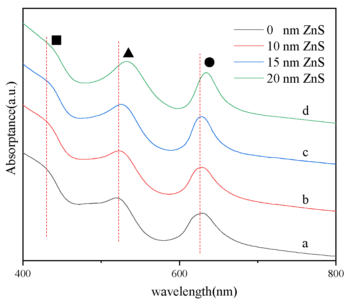
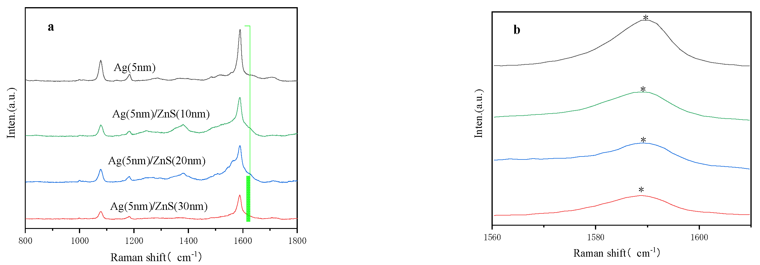
3. Results and Discussions
4. Conclusions
Author Contributions
Funding
Conflicts of Interest
References
- Ding, S.Y.; You, E.M.; Tian, Z.Q.; Moskovits, M. Electromagnetic theories of surface-enhanced Raman spectroscopy. Chem. Soc. Rev. 2017, 46, 4042–4076. [Google Scholar] [CrossRef] [PubMed]
- Wang, Y.H.; Zheng, S.; Yang, W.M.; Zhou, R.Y.; He, Q.F.; Radjenovic, P.; Dong, J.C.; Li, S.; Zheng, J.; Yang, Z.L.; et al. In situ Raman spectroscopy reveals the structure and dissociation of interfacial water. Nature 2021, 600, 81–85. [Google Scholar] [CrossRef] [PubMed]
- Chikan, V. Challenges and Prospects of Electronic Doping of Colloidal Quantum. J. Phys. Chem. Lett. 2011, 2, 2783–2789. [Google Scholar] [CrossRef]
- Ruddy, D.A.; Erslev, P.T.; Habas, S.E.; Seabold, J.A.; Neale, N.R. Surface Chemistry Exchange of Alloyed Germanium Nanocrystals: A Pathway toward Conductive Group IV Nanocrystal Films. J. Phys. Chem. Lett. 2013, 4, 416–421. [Google Scholar] [CrossRef]
- Tung, R.T. Chemical bonding and Fermi level pinning at metal-semiconductor interfaces. Phys. Rev. Lett. 2000, 84, 6078–6081. [Google Scholar] [CrossRef]
- Trang, T.N.Q.; Phan, T.B.; Nam, N.D.; Thu, V.T.H. In Situ Charge Transfer at the Ag@ZnO Photoelectrochemical Interface toward the High Photocatalytic Performance of H-2 Evolution and RhB Degradation. ACS Appl. Mater. Interf. 2020, 12, 12195–12206. [Google Scholar] [CrossRef]
- Willets, K.A.; Van Duyne, R.P. Localized surface plasmon resonance spectroscopy and sensing. Annu. Rev. Phys. Chem. 2007, 58, 267–297. [Google Scholar] [CrossRef] [Green Version]
- Freeman, R.G.; Grabar, K.C.; Allison, K.J.; Bright, R.M.; Davis, J.A.; Guthrie, A.P.; Hommer, M.B.; Jackson, M.A.; Smith, P.C.; Walter, D.G.; et al. Self-Assembled Metal Colloid Monolayers: An Approach to SERS Substrates. Science 1995, 267, 1629–1632. [Google Scholar] [CrossRef]
- Li, J.F.; Huang, Y.F.; Ding, Y.; Yang, Z.L.; Li, S.B.; Zhou, X.S.; Fan, F.R.; Zhang, W.; Zhou, Z.Y.; Wu, D.Y.; et al. Shell-isolated nanoparticle-enhanced Raman spectroscopy. Nature 2010, 464, 392–395. [Google Scholar] [CrossRef]
- Chang, Y.L.; Lai, I.C.; Lu, L.C.; Chang, S.W.; Sun, A.Y.; Wan, D.H.; Chen, H.L. Wafer-scale nanocracks enable single-molecule detection and on-site analysis. Biosen. Bioelectron. 2022, 200, 113920. [Google Scholar] [CrossRef]
- Xu, H.; Chen, Y.B.; Xu, W.G.; Zhang, H.L.; Kong, J.; Dresselhaus, M.S.; Zhang, J. Modulating the Charge-Transfer Enhancement in GERS using an Electrical Field under Vacuum and an n/p-Doping Atmosphere. Small 2011, 7, 2945–2952. [Google Scholar] [CrossRef] [PubMed]
- Li, P.; Ge, M.H.; Cao, C.T.; Lin, D.Y.; Yang, L.B. High-affinity Fe3O4/Au probe with synergetic effect of surface plasmon resonance and charge transfer enabling improved SERS sensing of dopamine in biofluids. Analyst 2019, 144, 4526–4533. [Google Scholar] [CrossRef] [PubMed]
- Ma, N.; Chen, L.; Jing, T.; Zhang, X.Y.; Han, B.B.; Xue, X.X.; Zhang, Y.J.; Zhao, B. New Insight into Charge-Transfer Enhancement for SERS in Cosputtering (Ag)x(ZnS)y System: The Carrier Density Effect. J. Phys. Chem. C 2019, 123, 28846–28851. [Google Scholar] [CrossRef]
- Fang, X.S.; Zhai, T.; Gautam, U.K.; Li, L.; Wu, L.; Bando, Y.; Golberg, D. ZnS nanostructures: From synthesis to applications. Prog. Mater. Sci. 2011, 56, 175–287. [Google Scholar] [CrossRef]
- Lee, G.J.; Wu, J.J. Recent developments in ZnS photocatalysts from synthesis to photocatalytic applications—A review. Powder Technol. 2017, 318, 8–22. [Google Scholar] [CrossRef]
- Kim, Y.; Coy, E.; Kim, H.; Mrowczynski, R.; Torruella, P.; Jeong, D.W.; Choi, K.S.; Jang, J.H.; Song, M.Y.; Jang, D.J.; et al. Efficient photocatalytic production of hydrogen by exploiting the polydopamine-semiconductor interface. Appl. Catal. B Environ. 2021, 280, 119423. [Google Scholar] [CrossRef]
- Suh, Y.H.; Lee, S.; Jung, S.M.; Bang, S.Y.; Yang, J.J.; Fan, X.B.; Zhan, S.J.; Samarakoon, C.; Jo, J.W.; Kim, Y.; et al. Engineering Core Size of InP Quantum Dot with Incipient ZnS for Blue Emission. Adv. Opt. Mater. 2022, 10, 2102372. [Google Scholar] [CrossRef]
- Sun, Q.; Wang, Y.A.; Li, L.S.; Wang, D.Y.; Zhu, T.; Xu, J.; Yang, C.H.; Li, Y.F. Bright, multicoloured light-emitting diodes based on quantum dots. Nat. Photonics 2007, 1, 717–722. [Google Scholar] [CrossRef]
- Zhang, Y.J.; Zhu, A.N.; Wang, Y.X.; Zhang, X.L. Plasmonic structure with nanocavity cavities for SERS detection of pesticide thiram. Nanotechnology 2021, 32, 135301. [Google Scholar] [CrossRef]
- Zhu, A.N.; Zhang, F.; Gao, R.X.; Zhao, X.Y.; Chen, L.; Zhang, Y.J.; Zhang, X.L.; Wang, Y.X. Increasing polarization-dependent SERS effects by optimizing the axial symmetry of plasmonic nanostructures. Appl. Surf. Sci. 2021, 494, 87–93. [Google Scholar] [CrossRef]
- Bellucci, S.; Bolesta, I.; Guidi, M.C.; Karbovnyk, I.; Lesivciv, V.; Micciulla, F.; Pastore, R.; Popov, A.I.; Velgosh, S. Cadmium clusters in CdI2 layered crystals: The influence on the optical properties. J. Phys. Condens. Matter 2007, 19, 395015. [Google Scholar] [CrossRef] [Green Version]
- Karbovnyk, I.; Lesivtsiv, V.; Bolesta, I.; Velgosh, S.; Rovetsky, I.; Pankratov, V.; Balasubramanian, C.; Popov, A.I. BiI3 nanoclusters in melt-grown CdI2 crystals studied by optical absorption spectroscopy. Phys. B 2013, 413, 12–14. [Google Scholar] [CrossRef]
- Liyanage, T.; Nagaraju, M.; Johnson, M.; Muhoberac, B.B.; Sardar, R. Reversible Tuning of the Plasmoelectric Effect in Noble Metal Nanostructures Through Manipulation of Organic Ligand Energy Levels. Nano Lett. 2020, 20, 192–200. [Google Scholar] [CrossRef] [PubMed]
- Yu, Z.; Yu, W.L.; Xing, J.; Ganeev, R.A.; Xin, W.; Cheng, J.L.; Guo, C.L. Charge transfer effects on resonance-enhanced Raman scattering for molecules adsorbed on single-crystalline perovskite. ACS Photonics 2018, 5, 1619–1627. [Google Scholar] [CrossRef]
- Wang, Y.X.; Yan, C.; Chen, L.; Zhang, Y.J.; Yang, J.H. Controllable charge transfer in Ag-TiO2 composite structure for SERS application. Nanomaterials 2017, 7, 159. [Google Scholar] [CrossRef]


Publisher’s Note: MDPI stays neutral with regard to jurisdictional claims in published maps and institutional affiliations. |
© 2022 by the authors. Licensee MDPI, Basel, Switzerland. This article is an open access article distributed under the terms and conditions of the Creative Commons Attribution (CC BY) license (https://creativecommons.org/licenses/by/4.0/).
Share and Cite
Zhang, Y.; Zhou, H.; Liang, L. Charge Transfer in Patterned Bilayer Film of Ag/ZnS Composite by Magnetron Control Sputtering. Molecules 2022, 27, 3805. https://doi.org/10.3390/molecules27123805
Zhang Y, Zhou H, Liang L. Charge Transfer in Patterned Bilayer Film of Ag/ZnS Composite by Magnetron Control Sputtering. Molecules. 2022; 27(12):3805. https://doi.org/10.3390/molecules27123805
Chicago/Turabian StyleZhang, Yongjun, Hailong Zhou, and Lijun Liang. 2022. "Charge Transfer in Patterned Bilayer Film of Ag/ZnS Composite by Magnetron Control Sputtering" Molecules 27, no. 12: 3805. https://doi.org/10.3390/molecules27123805