Article

Inherently Area-Selective Atomic Layer Deposition of Manganese Oxide through Electronegativity-Induced Adsorption

1
State Key Laboratory of Digital Manufacturing Equipment and Technology, School of Mechanical Science and Engineering, Huazhong University of Science and Technology, 1037 Luoyu Road, Wuhan 430063, China
2
State Key Laboratory of Materials Processing and Die & Mould Technology, School of Materials Science and Engineering, Huazhong University of Science and Technology, 1037 Luoyu Road, Wuhan 430063, China
*
Authors to whom correspondence should be addressed.
Molecules 2021, 26(10), 3056; https://doi.org/10.3390/molecules26103056
Submission received: 14 April 2021 / Revised: 16 May 2021 / Accepted: 17 May 2021 / Published: 20 May 2021
(This article belongs to the Special Issue Self-Assembled Materials and Bottom-Up Fabrication)

Abstract

:
Manganese oxide (MnOx) shows great potential in the areas of nano-electronics, magnetic devices and so on. Since the characteristics of precise thickness control at the atomic level and self-align lateral patterning, area-selective deposition (ASD) of the MnOx films can be used in some key steps of nanomanufacturing. In this work, MnOx films are deposited on Pt, Cu and SiO2 substrates using Mn(EtCp)2 and H2O over a temperature range of 80–215 °C. Inherently area-selective atomic layer deposition (ALD) of MnOx is successfully achieved on metal/SiO2 patterns. The selectivity improves with increasing deposition temperature within the ALD window. Moreover, it is demonstrated that with the decrease of electronegativity differences between M (M = Si, Cu and Pt) and O, the chemisorption energy barrier decreases, which affects the initial nucleation rate. The inherent ASD aroused by the electronegativity differences shows a possible method for further development and prediction of ASD processes.

Graphical Abstract

1. Introduction

Area-selective deposition (ASD), including area-selective atomic layer deposition (ALD), is considered a prospective way to downscale nano-electronics [1,2,3]. ALD takes advantage of self-limiting reactions to achieve conformal thin film growth with atomic-level thickness control [4]. The ALD reactions are extremely sensitive to surface chemistry due to the self-limiting nature [5]. Firstly, the activity of the precursors and steric hindrance from the ligands affect the density of chemisorption [6]. Meanwhile, the type and density of surface-active sites have an important role in the growth rate of target materials [7]. It is generally considered that the O*, H* and –OH are the active sites for the precursors’ chemisorption [8,9,10]. In some conditions, the byproducts or impurities may poison the surface and prevent additional adsorption of the precursors [11,12]. Moreover, a surface with catalytic activity can promote ALD growth [13,14]. When the driving force of nucleation is between the Gibbs free energy barriers of two different surfaces, the nuclei form rapidly on a surface with a low-energy barrier rather than on the other. Thus, ideal area-selective ALD can be realized through nuclei inhibition on the nongrowth areas. The selective deposition is quite complicated and relies on the coupled parameters, including substrates, precursors, temperature, pressure and aspect ratio dependency. Prior reports showed that the selectivity could be obtained by chemical modification, including surface passivation with polymers, self-assembled monolayers (SAMs), inhibitors and so on [15,16,17]. The above methods achieve high selectivity for nano-feature patterning but have limitations in long passivation time and complex steps. Thus, inherently selective deposition has been investigated to relax process complexity [18]. Up to now, four types of ASD have been reported, including DoD, DoM, MoD and MoM (M = metal, D = dielectric). Among them, selective deposition of oxides on metal can be used as barrier or capping layers to improve device performance.
ALD-MnOx has been studied and utilized to reduce the overall interconnect resistance in microelectronics [19]. It was also applicable to energy storage and conversion [20], magnetic devices [21] and so on. Previous studies demonstrated that the manganese oxide was fabricated by ALD using bis(ethylcyclopentadienyl) manganese (Mn(EtCp)2) and water (H2O) [22,23] or tris(2,2,6,6-tetramethyl-3,5-heptanedionato) manganese (Mn(thd)3) and ozone (O3) [24] as precursors. The MnOx layer was conformally deposited in the high aspect-ratio structures, and the ~1 nm thin film showed great diffusion barrier properties [25]. Usually, the deposition took place on the entire surface and needed auxiliary etching to obtain nanopatterns. Kawasaki et al. found that the selective deposition of MnOx existed between Cu and low-k SiCOH films, and the nucleation delay on SiCOH films is just a few cycles [26]. Moreover, they found that the native oxide layer on Cu is in favor of an ALD reaction compared with non-oxidized Cu. Phuong et al. discovered that plasma-treated and as-received SiOC substrates had different deposition rates of MnOx [27]. It was found that moisture was adsorbed on the matrix after plasma treatment and acted as a catalyst for MnOx deposition. The chemical bond between the deposited oxide and the substrate is M–O–Mn (M = metal, metalloid), and the chemical state of the surface oxygen group is the key issue. Previous reports established a relationship between the type of oxygen species and the nucleation rate [28]. Therefore, it is of great significance to study the surface chemistry and reaction mechanism to obtain high selectivity.
In this article, MnOx is deposited on metal/SiO2 patterns using Mn(EtCp)2 precursors with H2O as co-reactant. The X-ray photoelectron spectroscopy (XPS) shows that the Mn (II) precursors are oxidized, and the substrates are reduced after the ALD process. Additionally, the surface oxygen group plays an important role in chemisorption. The selectivity is quantified by EDS mapping, and the selectivity is optimized by adjusting deposition temperature. Meanwhile, it was found that selectivity has a relationship with the electronegativity differences. The differences in electronegativity decrease in the order of Si–O (1.54), Cu–O (1.44) and Pt–O (1.16). On the contrary, the deposition rate is negatively related to the electronegativity differences. It is conducive to the formation of M–O–Mn (M = metal, metalloid) bonds in areas with a low difference in electronegativity.

2. Results

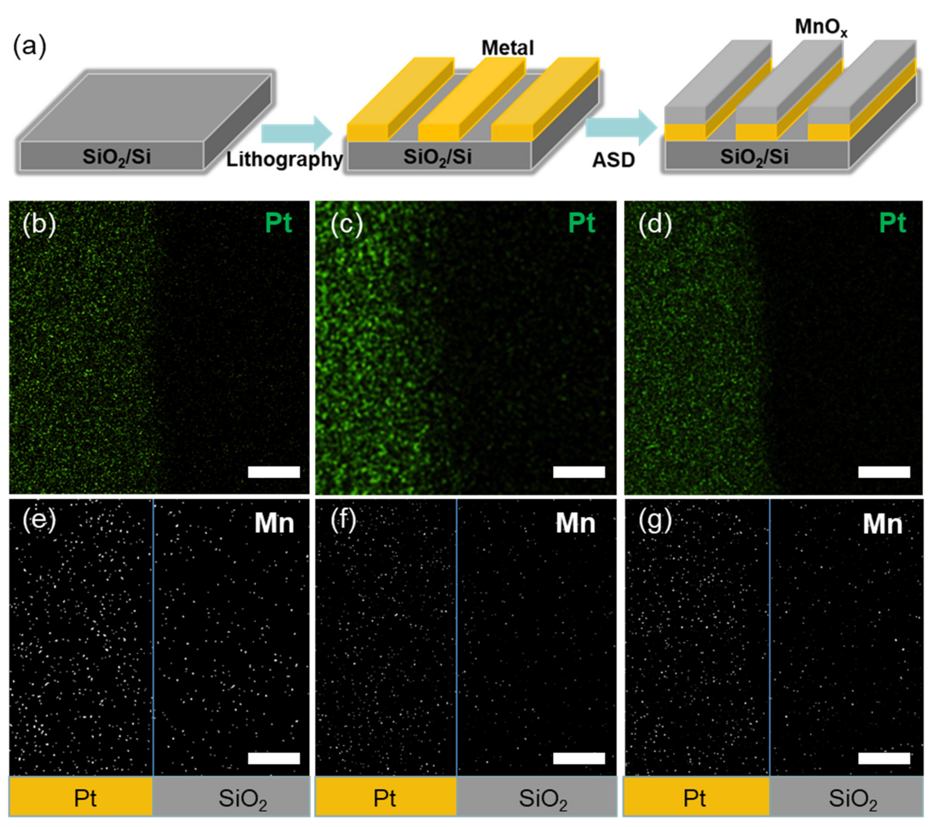
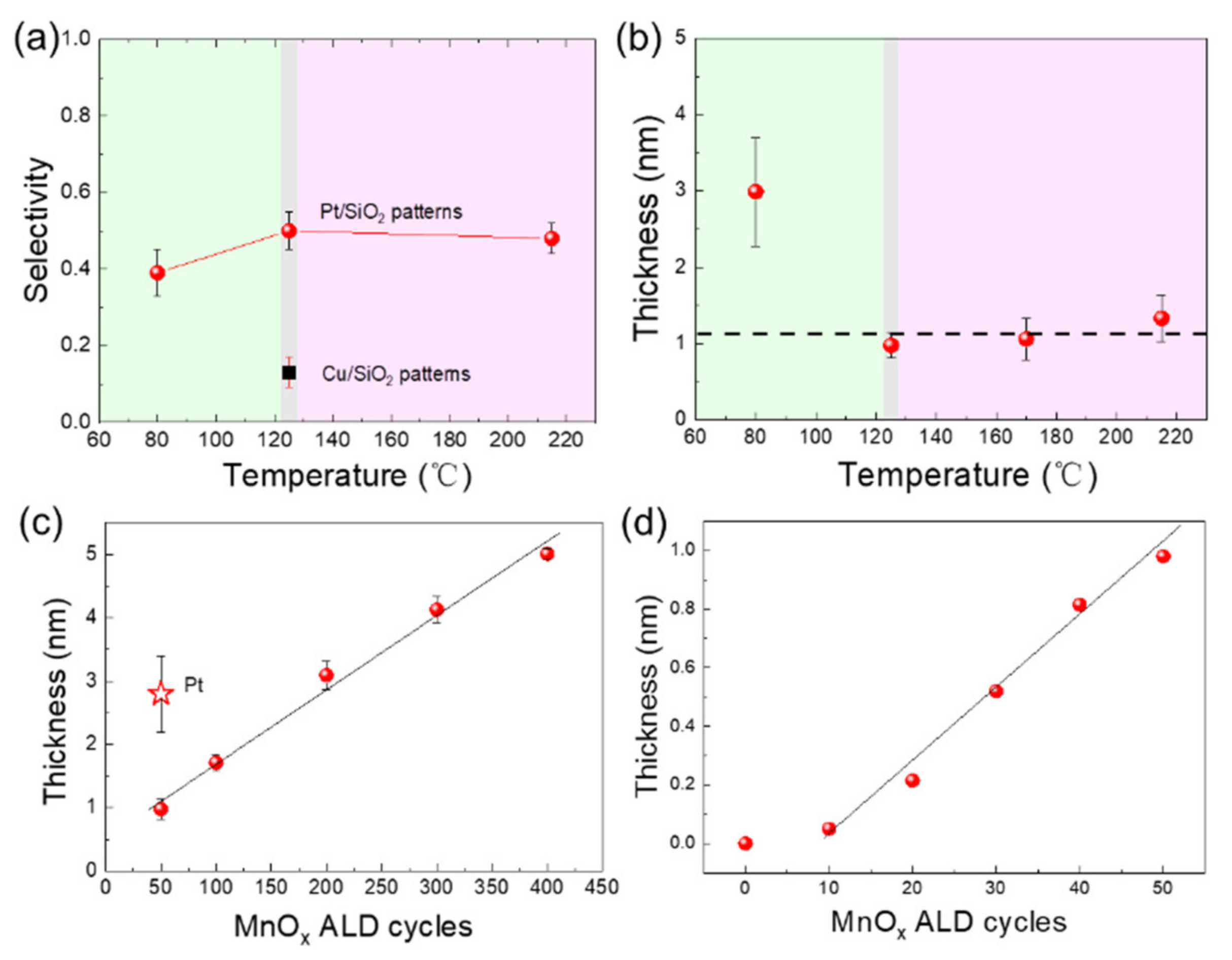
2.1. Characterization of Selectivity

The schematic diagram of MnOx deposited on metal/SiO2 patterns is shown in Figure 1a. The patterns consist of 60 μm metal-capped lines. There are sharp boundaries between the metal and exposed SiO2/Si areas (Figure S1 from Supplementary Materials). After 50 ALD MnOx cycles, the amplified border areas are characterized with SEM and EDS. Figure 1 shows EDS mapping of Pt and Mn on Pt/SiO2 patterns at 80, 125 and 215 °C, respectively. The green and white points represent Pt and Mn elements, respectively. It is found that the density of white points (Mn) on the Pt surface is higher than that on the SiO2/Si surface, indicating that MnOx grows faster on the Pt surface. The white points decrease on the nongrowth SiO2 regions with increasing deposition temperature, indicating that the selectivity is improved. The temperature adjustment can enlarge the differences in the deposition rates on different substrates. The quantitative values of selectivity and the corresponding selectivity window are presented in the following parts.

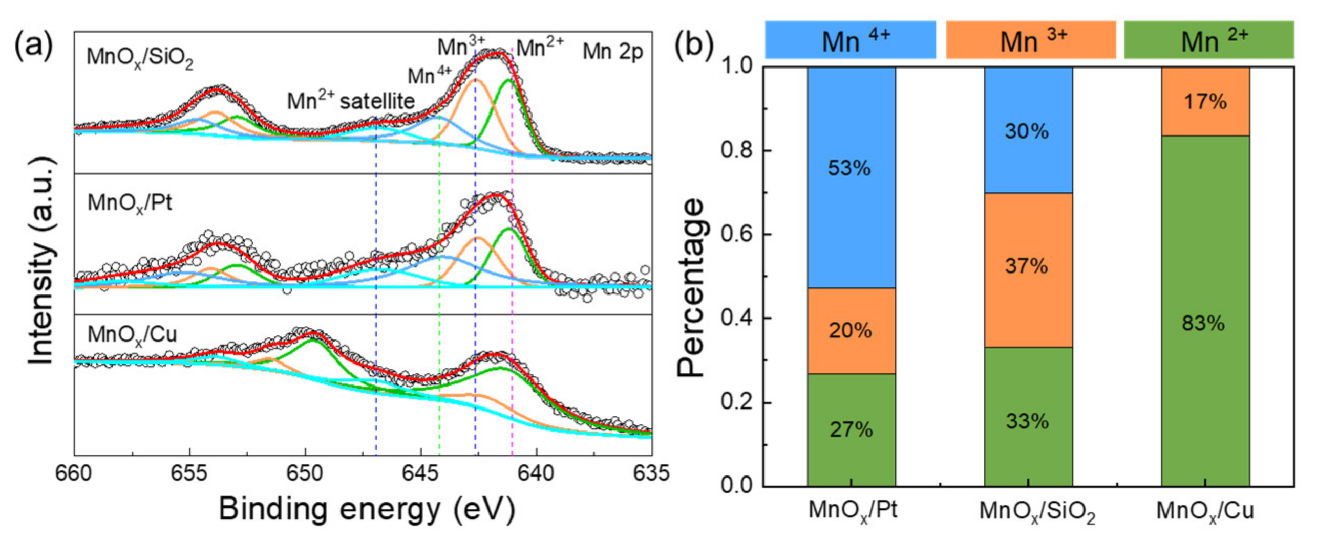
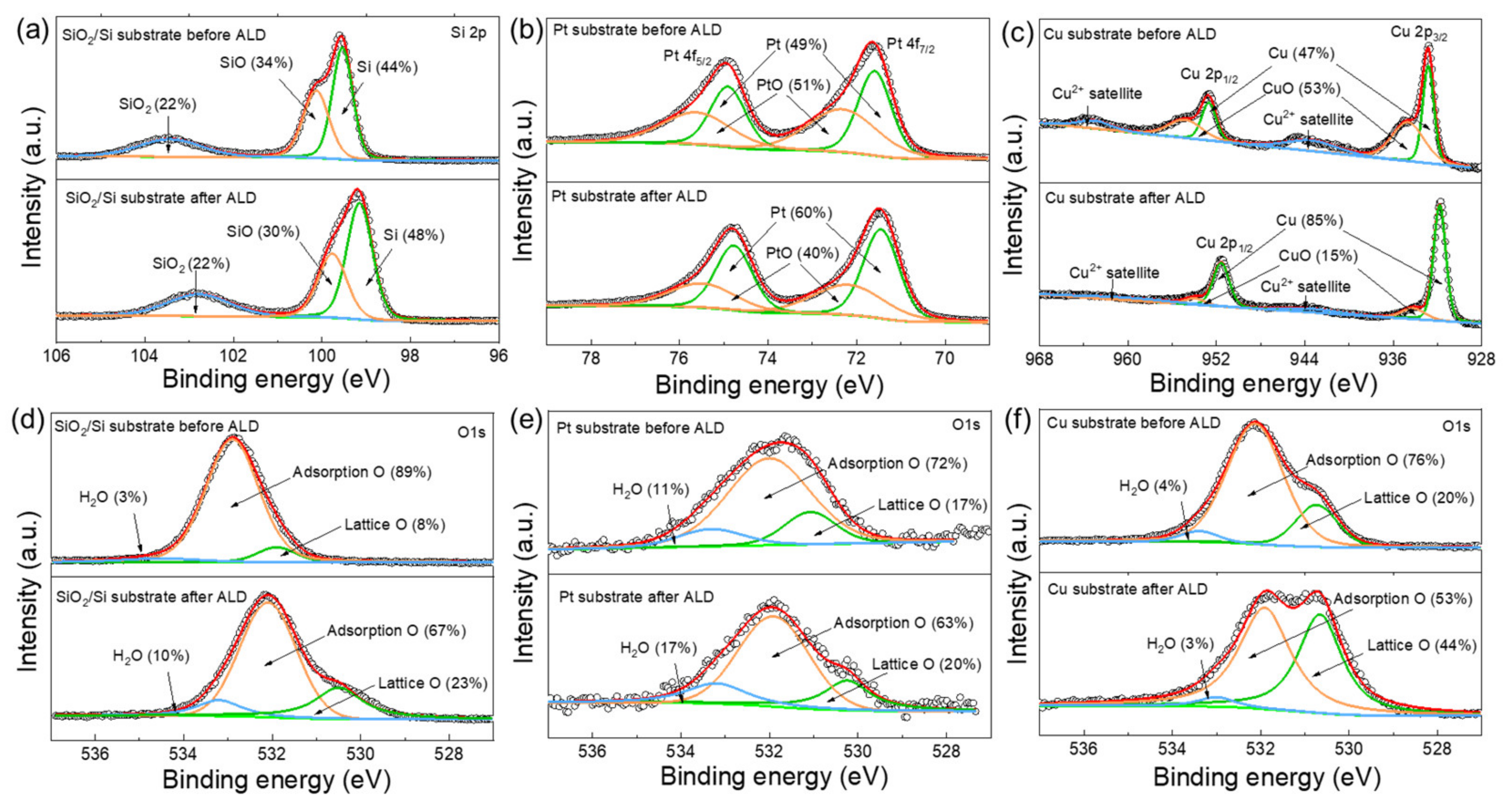
2.2. Surface Composition of MnOx Deposited on Different Substrates

The substrates’ surfaces affect nucleation behaviors of selective deposition and subsequent quality of target materials. To identify the influences of surface species during ALD, the composition of MnOx deposited on Pt, Cu and SiO2 substrates are analyzed by XPS. Firstly, the appearance of Mn peak indicates that MnOx is grown on three kinds of substrates. The Mn 2p spectrum (Figure 2a) shows two peaks corresponding to the Mn 2p3/2 and Mn 2p1/2 core levels centered at binding energies of ~653.0 eV and ~642.0 eV, respectively [29,30]. After the spectra fitting analysis, the Mn 2p3/2 spectra are separated with four peaks located at around 641.1–641.3 eV, 642.1–642.6 eV, 644.0–644.3 eV and 646.5–647.0 eV, which correspond to Mn2+, Mn3+, Mn4+ and Mn2+ satellite bonds, respectively. It is found that there are three valence states of Mn element on Pt and SiO2 surface, while there is no tetravalent Mn on Cu surface.
The Mn(EtCp)2 precursor is a reducing agent due to its unsaturated –EtCp ligands. Thus, the MnOx film presents higher valences due to oxidation during the ALD process. The percentage of tetravalent Mn on Pt is higher than that on the SiO2 surface. This is perhaps because of the catalytic activity of Pt. Previous studies attributed ASD of metal oxides (such as FeOx, CeOx) on Pt/SiO2 patterns to catalytic activation of oxygen that increase nucleation rate on Pt [31]. Due to the high activity of surface oxygen species on Pt, it is easier for the precursor’s adsorption and decomposition, thus leading to high selectivity.
To analyze the role of surface oxygen species, the SiO2/Si, Pt and Cu substrates before and after MnOx deposition are measured with XPS and presented in Figure 3. All of the substrates are reduced in a 10% hydrogen mixture at 125 °C, and then the substrates are transferred into the ALD reactor to deposit MnOx. It is found that Pt and Cu substrates are partially oxidized before the ALD process, although the substrates are already reduced. Hence, surface oxygen species will affect the nucleation behaviors during selective deposition. After 50 ALD cycles, Pt is slightly reduced, while the Cu substrate is obviously reduced (Figure 3b,c). The electron transfer occurs between the substrate and the Mn precursors, which results in the reduction of the substrate [30]. The surface oxygen species act as active sites for MnOx deposition. The rapid disappearance of CuO may lead to a great decrease of active sites and the weakening of the electron-stripping ability of the substrate, resulting in the absence of tetravalent manganese. Additionally, the O 1s XPS spectrum of SiO2/Si, Pt and Cu substrates are presented. After the MnOx deposition, the content of lattice oxygen is more than that of the bare substrate without deposition. The increase of lattice oxygen may contribute to the Mn–O bonds after deposition.

2.3. Selectivity Window of MnOx

To obtain high selectivity, it is necessary to suppress nuclei on the nongrowth areas. To quantify the selectivity, Equation (1) is as follows [32]:
Selectivity = θ G A θ N G A θ G A + θ N G A
where θGA and θNGA are the amount of target materials deposited on the growth and nongrowth areas, respectively. In the experiments, θ is simplified as the number of white points (Mn) per unit area in EDS mappings. The larger the number of white points of Mn, the more MnOx deposited on the substrate. Thus, EDS mapping can be used as a semi-quantitative method to acquire the values of selectivity.
Through mathematical counting of Mn EDS mapping in Figure 1, the quantitative selectivity values are obtained. The selectivity on Pt/SiO2 patterns increases from 0.39 to 0.5 through increasing temperature from 80 to 125 °C. Then, the selectivity slightly decreases to 0.48 at 215 °C (Figure 4a). The selectivity between Cu and SiO2 surface is also analyzed, and there is almost no selective growth.
To study the relationship between the selectivity and the ALD temperature window, the growth rate is evaluated at the same temperature range (Figure 4b). As the deposition temperature increases from 80 to 125 °C, the growth rate of Mn oxides decreases quickly (50 ALD cycles are exploited). Further increasing the deposition temperature has minimal influence on film thickness, indicating that the temperatures ranging from 125 to 215 °C are within the ALD window. It is found that high selectivity can be obtained only in the ALD window. The Mn precursors may condense at 80 °C, which causes weak selectivity.
The MnOx film thickness increases linearly on SiO2 substrate after 50 cycles (Figure 4c). The steady growth rate is 0.01 nm/cycle at 125 °C. The slow nucleation on the SiO2 regions is thought to be beneficial to achieve selective deposition. The growth rate within 50 ALD cycles is also presented in Figure 4d. The first 50 ALD cycles show two growth stages: ~10 cycles of nucleation incubation and a rapid growth stage indicating the acceleratory growth of nuclei islands. After 50 cycles, the surface of the SiO2 substrate is almost covered, and the nuclei islands begin to coalesce. The growth rate remains stable when further increasing ALD cycles. The surface gradually changes from SiO2 to MnOx layer after approximately 50 cycles, and the deposition rate decreases. When all the surfaces are completely covered with MnOx, the substrate differences between Pt, Cu and SiO2 are limited. For MnOx grown on ultrathin Pt films, it is found that the film thickness is ~2.8 nm at 50 ALD cycles, which is much higher than that on the SiO2 substrate. The nucleation stage is also studied by examining the surface morphology of ALD MnOx ultrathin films with SEM and AFM (Figure S2 from Supplementary Materials). SEM image shows that there are a lot of nuclei islands on SiO2 at 50 ALD cycles. After 400 ALD cycles, the particle size increases from ~9.1 to ~16.7 nm. AFM images show that initial MnOx deposition increases the surface roughness, then it decreases slowly from ~0.80 to ~0.64 nm with increasing ALD cycles (see Figure S3 from Supplementary Materials).
The GPC is also checked by changing the pulse time of the precursors. The critical time of saturated adsorption of Mn precursors and water are ~2 and ~3 s, respectively (Figure S4a,b from Supplementary Materials). After the minimum dose time, the thickness maintains at 0.9~1.0 nm with increasing dosing time. It is found that the purge times longer than 30 and 60 s are enough to remove excess Mn(EtCp)2 and H2O, respectively. The long pulse time of Mn(EtCp)2 (3s) and H2O (3s) in this work are to ensure sufficient adsorption and decomposition. The above results exhibit good self-limiting character, which lays a foundation for selective growth.

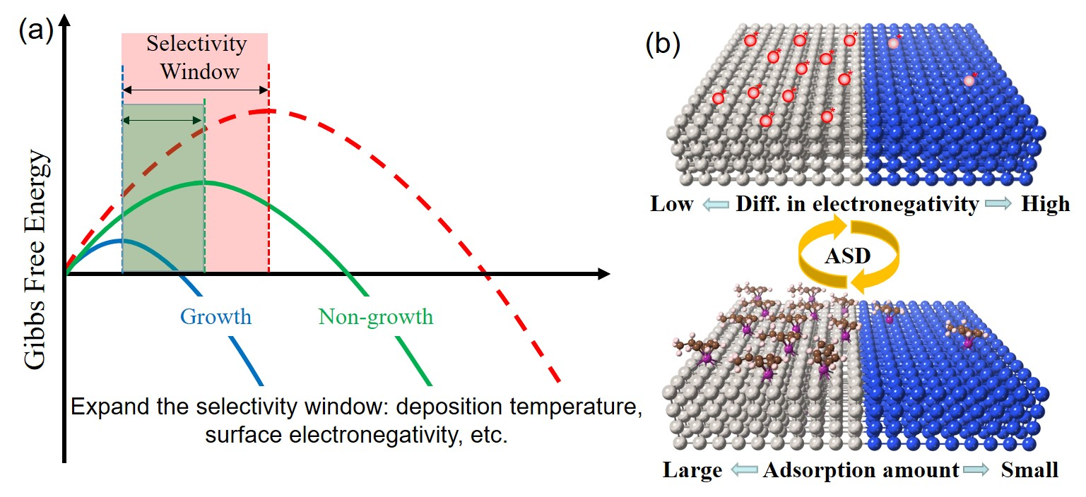
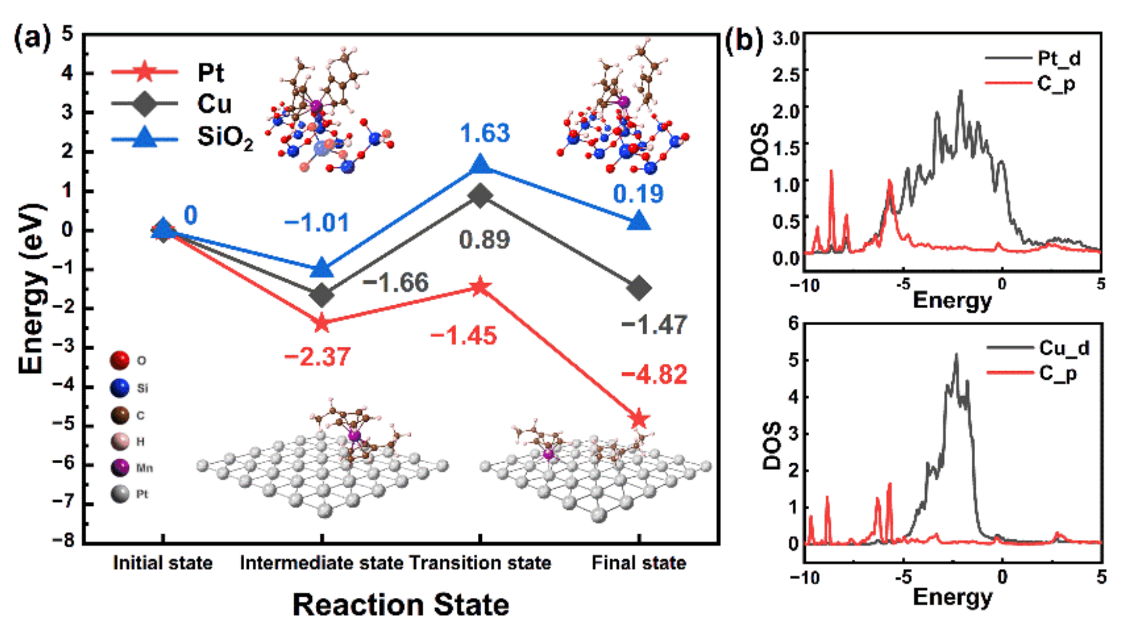
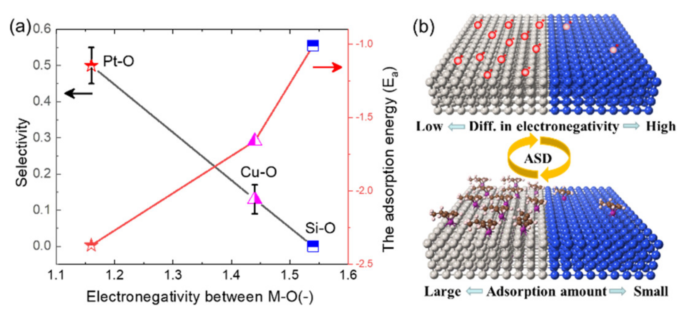
3. The Origin of Selective Growth

It is considered that ASD is mainly originated from competition between surface chemisorption, decomposition and so on [33]. To elucidate the origin of selective growth, the density functional theory (DFT) and nudged elastic band (NEB) are adopted to calculate the decomposition energy and energy barriers of ALD precursors on Pt, Cu and SiO2 surfaces, as shown in Figure 5a. On the SiO–OH surface, the following reactions between Mn(EtCp)2 and surface are considered as Equation (2) [34,35,36]:
Mn(EtCp)2 + ‖–OH=‖–O–Mn(EtCp) + H–EtCp
According to the previous study, the following decomposition reactions on the surface of Pt and Cu are considered as Equation (3) [37,38]:
Mn(EtCp)2 + ‖–O=‖–O–Mn(EtCp) + ‖–O–EtCp
Firstly, the adsorption energy of Mn precursor on three different substrates is analyzed. On the surface of SiO2, Mn(EtCp)2 is adsorbed on the –OH sites, and the adsorption energy is −1.01 eV. In the decomposition step, the EtCp group combines with the H atom of –OH to form H-EtCp, and the decomposition energy barrier is 2.64 eV. Mn(EtCp)2 is adsorbed on Pt and Cu surfaces with EtCp ligand facing the surface, and the adsorption energies are −1.66 and −2.37 eV, respectively. The Mn-EtCp part slips from the EtCp group to the Pt and Cu surfaces, and the decomposition barriers are 0.92 and 2.55 eV, respectively.
The above results reveal that the growth of Mn(EtCp)2 has priority in the order of Pt > Cu > SiO2. Then, the partial density of states (PDOS) of precursors adsorbed on Pt and Cu surface is analyzed (Figure 5b). From the PDOS diagram, the overlap of C_p orbital and Pt_d orbit indicates that a strong chemical bond is formed between the Pt surface and the precursors. In contrast, such an orbital overlap is absent on the Cu surface. The preferential growth of MnOx on the Pt surface may come from the favorable adsorption and decomposition process of Mn precursors.
To further explore the effect of substrates, the relationship between the selectivity and differences in electronegativity between M and O is presented (Figure 6a). The Pauling electronegativity of Pt, Cu, Si and O are 2.28, 2.00, 1.90 and 3.44, respectively [39]. The differences in electronegativity between M (M = Pt, Cu and Si) and O decrease in the order of Si–O (1.54), Cu–O (1.44) and Pt–O (1.16). It is found that selectivity is negatively correlated with the differences in electronegativity. Smaller differences in electronegativity between M–O may lead to weaker bonding energy [40,41], which may influence the chemisorption of Mn precursors on Si–O, Cu–O and Pt–O surfaces. The absolute value of adsorption energy rises with the order of Si–O, Cu–O and Pt–O from the DFT calculations, and the reaction barrier decreases with the same order. The differences in electronegativity may also become a supplemental explanation of selectivity for some precursors on certain substrates. The origin of selective deposition is the differences in chemisorption between two surfaces. At the nucleation stage, the precursors are chemically adsorbed on the surface oxygen groups to form M–O–Mn bonds. The bonding energy of M–O, which is affected by the electronegativity, thus affects chemical adsorption. Smaller differences in electronegativity between M–O may lead to weak bonding, which is beneficial to reduce the reaction barrier.

4. Materials and Methods

4.1. Substrate Preparation

Cu and Pt films were deposited by sputtering onto Si(100) wafers using an argon-based plasma. The film thickness is a few nanometers. The surface roughness of the Pt and Cu substrates are less than 5 nm. Si (100) substrates, with a layer of SiO2 around 20 Å thick, were cleaned with acetone and deionized water. The Pt and Cu samples were annealed in hydrogen to remove the oxide layers as much as possible. If they were not immediately used after cleaning, the substrates are stored in the argon atmosphere until use.

4.2. Growth Conditions

The ALD reactions were performed in a custom hot-walled ALD reactor (Material Design and Nano-manufacturing center @ HUST, Wuhan, China) at 50−250 °C, and 50 Pa of argon pressure provided by an 80 Sccm continuous argon purge (99.999%, Prepurified). ALD of MnOx was carried out using (a) Mn(EtCp)2 (>98%, Aimou Yuan, Nanjing, China) and (b) H2O (ultrapure deionized water). The temperature of the precursor’s container was controlled at 100 °C, in which argon was diverted over the headspace of the liquid precursors during dosing. The temperature of the pipeline was 20 °C higher than that of the container to prevent condensation of Mn precursors. The inset of Figure S4a (from Supplementary Materials) shows the typical half-reactions process of Mn(EtCp)2 and H2O dosing. The base pressure of the ALD chamber was about ~113 Pa, the peak pressure of the Mn(EtCp)2 and H2O dose were tuned to a level of ~20 and ~7 Pa above the base pressure, respectively. The ALD reactions were carried out in a circulate of Mn(EtCp)2, purge, H2O and purge sequence, with a typical time of 3, 30, 3, and 60 s.

4.3. Characterization of MnOx

The film thickness on SiO2 was measured by a spectroscopic ellipsometer (SE, M-200X, J. A. Woollam Co., Inc., Lincoln, NE, USA). Additionally, MnOx thickness on ALD Pt was acquired by SE after 50 ALD cycles at 125 °C. The wavelength of light ranged from 250 to 1000 nm. The software was Complete EASE, and a modified Cauchy model was used to fit the ellipsometer data. Patterned Pt/SiO2 and Cu/SiO2 substrates were observed by optical microscope. The surface morphology was analyzed by SEM (attached EDS, SU3900, HITACHI, Tokyo, Japan) and AFM (Agilent 5500, Santa Clara, CA, USA) for 0, 50 and 400 MnOx ALD cycles. EDS mappings of platinum and manganese were measured on Pt/SiO2 patterns after 50 ALD MnOx cycles at 80, 125, and 215 °C. The surface composition was evaluated by X-ray photoelectron spectrograph (XPS, AXIS-ULTRA DLD-600 W, Shimadzu-Kratos Co., Manchester, UK) with an Al Kα X-ray (hν = 1486.6 eV) after 50 ALD cycles on Cu, Pt and SiO2 substrates. All the spectrum were calibrated using C 1s (285 eV). The peaks were separated by XPS peak software, and the background was removed by Shirley type. The peak areas of Mn2+, Mn2+ satellite, Mn3+ and Mn4+ within Mn 2p3/2 were two times higher than that of Mn 2p1/2, respectively. The ratio of Lorentzian–Gaussian was 20%. The peak area represented the content of different bonds.

4.4. DFT Calculation

DFT calculations were carried out using the first-principles plane-wave pseudopotential formulation implemented in the Vienna ab-initio Simulation Package (version 5.4.4, University of Vienna, Vienna, Austria). The exchange−correlation functional was in the form of Perdew−Burke−Ernzerhof with the generalized gradient approximation [42]. Van der Waals interactions were also accounted to be based on experience. The cutoff energy was 400 eV on the basis of the plane-wave. A k-mesh of 3 × 3 × 1 was applied to ensure the energy convergence to 1 meV, and the residual force acting on each atom is less than 0.05 eV/Å. A 5 × 5 × 4 Pt(111) slabs model, 5 × 5 × 4 Cu(111) slabs model and 13 layers hydroxylated SiO2 slabs model was built to resemble the Pt, Cu and SiO2 surface on the experiment, respectively. The adsorption energy (Ea) of the precursor on the Pt surface was defined by the Equation (4) [38]:
Ea = E*ads − E* − EMn(EtCp)2
where E*ads is the total energy of the slabs; E* and EMn(EtCp)2 are the energies of the slabs and precursor molecule, respectively. The decomposition energy (Ed) is calculated by the Equation (5):
Ed = E*dec − E* − EMn(EtCp)2
where E*dec is the total energy of the surface with the precursor decomposed. The nudged elastic band (NEB) was used to search the minimum energy path (MEP) of the precursor dissociation on the Pt surface and locate the transition state between two local minima. Six intermediate images were interpolated between the adsorbed state and decomposed state.

5. Conclusions

In this work, MnOx films are fabricated with ALD using bis(ethylcyclopentadienyl) manganese (Mn(EtCp)2) and H2O. Inherently selective growth is demonstrated on patterned Pt/SiO2 and Cu/SiO2 substrates. It is found that MnOx preferential deposits on Pt, then followed by Cu and SiO2. The selectivity improves with increasing deposition temperature within the ALD window. Meanwhile, it is found that the calculated selectivity has a negative relationship with enlarging the electronegativity differences between M (M = Si, Cu and Pt) and O. The origin of selective deposition is the differences of chemisorption between two surfaces. The bonding energy of M−O is affected by the electronegativity, thus affects chemical adsorption. Smaller differences in electronegativity between M−O may lead to weak bonding, which is beneficial to reduce the reaction barrier. The differences in electronegativity may also become a supplemental explanation of selectivity for some precursors on certain substrates, which shows a possible method the further development and prediction of selective ASD processes.

Supplementary Materials

The following are available online, Figure S1: Optical images of patterned (a) Pt/SiO2 and (b) Cu/SiO2 substrate, SEM images of amplified (c) Pt/SiO2 and (d) Cu/SiO2 patterns after 50 ALD cycles. Figure S2: SEM images of (a) bare Si substrate; (b) 50 ALD MnOx cycles; (c) 400 ALD MnOx cycles; AFM images of (d) bare Si substrate; (e) 50 ALD MnOx cycles; (f) 400 ALD MnOx cycles. Figure S3: Surface roughness as a function of ALD MnOx cycles. Figure S4: Film thickness with respect to (a) Mn(EtCp)2 pulse time and (b) H2O pulse time. The inset in (a) is the pressure of dosing Mn(EtCp)2 and H2O as a function of time. The deposition temperature is 125 °C, for (a) and (b).

Author Contributions

Conceptualization, Y.-C.L., K.C. and R.C.; methodology, M.G.; software, Y.-X.L., Y.-W.W., B.S.; validation, J.-M.Z.; formal analysis, K.C.; data curation, Y.-C.L.; writing—original draft preparation, Y.-C.L.; writing—review and editing, Y.-C.L.; visualization, Y.-C.L.; supervision, K.C., R.C.; project administration, K.C.; funding acquisition, K.C., B.S. and R.C. All authors have read and agreed to the published version of the manuscript.

Funding

This work is supported by the National Natural Science Foundation of China (51835005, 51871103, and 51911540476), the Hubei Province Natural Science Foundation for innovative research groups (2020CFA030) and the Independent Innovation Research Fund of Huazhong University of Science and Technology (2019kfyXMBZ025).

Data Availability Statement

Not applicable.

Acknowledgments

The authors would also like to acknowledge the support from the Analytic Testing Center and the Flexible Electronics Research Center of the HUST.

Conflicts of Interest

The authors declare no conflict of interest.

Sample Availability

Samples of the compounds are available from the authors.

References

  1. Mackus, A.J.M.; Merkx, M.J.M.; Kessels, W.M.M. From the bottom-up: Toward area-selective atomic layer deposition with high selectivity. Chem. Mater. 2018, 31, 2–12. [Google Scholar] [CrossRef] [PubMed] [Green Version]
  2. Chen, R.; Li, Y.C.; Cai, J.M.; Cao, K.; Lee, H. Atomic level deposition to extend Moore’s law and beyond. Int. J. Extrem. Manuf. 2020, 2, 022002. [Google Scholar] [CrossRef]
  3. Parsons, G.N.; Clark, R.D. Area-selective deposition: Fundamentals, applications, and future outlook. Chem. Mater. 2020, 32, 4920–4953. [Google Scholar] [CrossRef]
  4. George, S.M. Atomic layer deposition: An overview. Chem. Rev. 2010, 110, 111–131. [Google Scholar] [CrossRef] [PubMed]
  5. Mackus, A.J.M.; Bol, A.A.; Kessels, W.M.M. The use of atomic layer deposition in advanced nanopatterning. Nanoscale 2014, 6, 10941–10960. [Google Scholar] [CrossRef] [Green Version]
  6. Adhikari, S.; Selvaraj, S.; Kim, D.H. Progress in powder coating technology using atomic layer deposition. Adv. Mater. Interfaces 2018, 1800581, 1–20. [Google Scholar] [CrossRef]
  7. Yanguas-Gil, A.; Libera, A.; Jeffrey, W.E. Modulation of the growth per cycle in atomic layer deposition using reversible surface functionalization. Chem. Mater. 2013, 25, 4849–4860. [Google Scholar] [CrossRef]
  8. Lu, J.; Low, K.B.; Lei, Y.; Libera, J.A.; Nicholls, A.; Stair, P.C.; Elam, J.W. Toward atomically-precise synthesis of supported bimetallic nanoparticles using atomic layer deposition. Nat. Commun. 2014, 5, 1–9. [Google Scholar] [CrossRef]
  9. Mameli, A.; Karasulu, B.; Verheijen, M.A.; Barcones, B.; Macco, B.; Mackus, A.; Kessels, M.; Roozeboom, F. Area-selective atomic layer deposition of ZnO by area activation using electron beam induced deposition. Chem. Mater. 2019, 31, 1250–1257. [Google Scholar] [CrossRef] [Green Version]
  10. Soethoudt, J.; Crahaij, S.; Conard, T.; Delabie, A. Impact of SiO2 surface composition on trimethylsilane passivation for area-selective deposition. J. Mater. Chem. C 2019, 7, 11911–11918. [Google Scholar] [CrossRef]
  11. Lu, J.L.; Elam, J.W. Low temperature ABC-type Ru atomic layer deposition through consecutive dissociative chemisorption, combustion, and reduction steps. Chem. Mater. 2015, 27, 4950–4956. [Google Scholar] [CrossRef]
  12. Masango, S.S.; Peng, L.; Marks, L.D.; Duyne, R.P.V.; Stair, P.C. Nucleation and growth of silver nanoparticles by AB and ABC-type atomic layer deposition. J. Phys. Chem. C 2014, 118, 17655–17661. [Google Scholar] [CrossRef]
  13. Weber, M.J.; Mackus, A.; Verheijen, M.A.; Marel, C.; Kessels, W. Supported core/shell bimetallic nanoparticles synthesis by atomic layer deposition. Chem. Mater. 2012, 24, 2973–2977. [Google Scholar] [CrossRef]
  14. Weber, M.J.; Verheijen, M.A.; Bol, A.A.; Kessels, W.M.M. Sub-nanometer dimensions control of core shell nanoparticles prepared by atomic layer deposition. Nanotechnology 2015, 26, 094002. [Google Scholar] [CrossRef] [PubMed] [Green Version]
  15. Bobb-Semple, D.; Nardi, K.L.; Draeger, N.; Hausmann, D.M.; Bent, S.F. Area-selective atomic layer deposition assisted by self-assembled monolayers a comparison of Cu, Co, W, and Ru. Chem. Mater. 2019, 31, 1635–1645. [Google Scholar] [CrossRef]
  16. Merkx, M.J.M.; Vlaanderen, S.; Faraz, T.; Verheijen, M.A.; Kessels, W.M.M.; Mackus, A.J.M. Area-selective atomic layer deposition of TiN using aromatic inhibitor molecules for metal/dielectric selectivity. Chem. Mater. 2020, 32, 7788–7795. [Google Scholar] [CrossRef]
  17. Cian, C.; Tobias, W.; Morris, M.A. Enabling large-area selective deposition on metal-dielectric patterns using polymer brush deactivation. J. Phys. Chem. C 2018, 122, 14698–14705. [Google Scholar]
  18. Cao, K.; Cai, J.; Chen, R. Inherently selective atomic layer deposition and applications. Chem. Mater. 2020, 32, 2195–2207. [Google Scholar] [CrossRef]
  19. Wang, Y.P.; Wu, X.; Liu, W.J.; Zhang, D.W.; Ding, S.J. Plasma-enhanced atomic layer deposition of low resistivity and ultrathin manganese oxynitride films with excellent resistance to copper diffusion. ACS Appl. Electron. Mater. 2020, 2, 1653–1660. [Google Scholar] [CrossRef]
  20. Choi, J.; Byun, W.J.; Kang, D.H.; Lee, J.K. Porous manganese oxide networks as high-capacity and high-rate anodes for Lithium-Ion batteries. Energies 2021, 14, 1299. [Google Scholar] [CrossRef]
  21. Seo, W.S.; Jo, H.H.; Lee, K.; Kim, B.; Oh, S.J.; Park, J.T. Size-dependent magnetic properties of colloidal Mn3O4 and MnO nanoparticles. Angew. Chem. Int. Ed. 2004, 116, 1135–1137. [Google Scholar] [CrossRef]
  22. Burton, B.B.; Fabreguette, F.H.; George, S.M. Atomic layer deposition of MnO using bis(ethylcyclopentadienyl)manganese and H2O. Thin Solid Films 2009, 517, 5658–5665. [Google Scholar] [CrossRef]
  23. Young, M.J.; Hare, C.D.; Musgrave, C.B.; George, S.M. Rapid growth of crystalline Mn5O8 by self-limited multilayer deposition using Mn(EtCp)2 and O3. ACS Appl. Mater. Interfaces 2016, 8, 18560–18569. [Google Scholar] [CrossRef] [PubMed]
  24. Nieminen, H.E.; Miikkulainen, V.; Settipani, D.; Simonelli, L.; Hönicke, P.; Zech, C.; Kayser, Y.; Beckhoff, B.; Honkanen, A.; Heikkilä, M.J.; et al. Intercalation of Lithium ions from gaseous precursors into β-MnO2 thin films deposited by atomic layer deposition. J. Phys. Chem. C 2019, 123, 15802–15814. [Google Scholar] [CrossRef] [Green Version]
  25. Koike, J.; Hosseini, M.; Hai, H.T.; Ando, D.; Sutou, Y. Material innovation for MOL, BEOL, and 3D Integration. IEDM 2017, 32, 1–4. [Google Scholar]
  26. Kawasaki, H.; Matsumoto, K.; Nagai, H.; Kikuchi, Y.; Chang, P. Atomic Layer Deposition of MnOx for Cu Capping Layer in Cu/low-k Interconnects. In Proceedings of the IEEE International Interconnect Technology Conference, San Jose, CA, USA, 20–23 May 2014; pp. 315–318. [Google Scholar]
  27. Phuong, N.M.; Sutou, Y.; Koike, J. Structural characterization of a manganese oxide barrier layer formed by chemical vapor deposition for advanced interconnects application on SiOC dielectric substrates. J. Phys. Chem. C 2013, 117, 160–164. [Google Scholar] [CrossRef]
  28. Maeda, E.; Nabatame, T.; Hirose, M.; Inoue, M.; Ohi, A.; Ikeda, N.; Kiyono, H. Correlation between SiO2 growth rate and difference in electronegativity of metal-oxide underlayers for plasma enhanced atomic layer deposition using tris(dimethylamino)silane precursor. J. Vac. Sci. Technol. A 2020, 38, 032409. [Google Scholar] [CrossRef]
  29. Mattelaer, F.; Vereecken, P.M.; Dendooven, J.; Detavernier, C. Deposition of MnO anode and MnO2 cathode thin films by plasma enhanced atomic layer deposition using the Mn(thd)3 precursor. Chem. Mater. 2015, 27, 3628–3635. [Google Scholar] [CrossRef]
  30. Yang, J.; Cao, K.; Gong, M.; Shan, B.; Chen, R. Atomically decorating of MnOx on palladium nanoparticles towards selective oxidation of benzyl alcohol with high yield. J. Catal. 2020, 386, 60–69. [Google Scholar] [CrossRef]
  31. Singh, J.A.; Thissen, N.F.W.; Kim, W.; Johnson, H.; Kessels, W.M.M.; Bol, A.A.; Bent, S.F.; Mackus, A.J.M. Area-selective atomic layer deposition of metal oxides on noble metals through catalytic oxygen activation. Chem. Mater. 2018, 30, 663–670. [Google Scholar] [CrossRef] [Green Version]
  32. Parsons, G.N. Functional model for analysis of ALD nucleation and quantification of area-selective deposition. J. Vac. Sci. Technol. A 2019, 37, 020911. [Google Scholar] [CrossRef]
  33. Grillo, F.; Soethoudt, J.; Marques, E.A.; Martín, L.; Dongen, K.V.; Ommen, J.R.; Delabie, A. Area-selective deposition of Ruthenium by area-dependent surface diffusion. Chem. Mater. 2020, 32, 9560–9572. [Google Scholar] [CrossRef]
  34. Mameli, A.; Kuang, Y.; Aghaee, M.; Ande, C.K.; Karasulu, B.; Creatore, M.; Mackus, A.J.M.; Kessels, W.M.M.; Roozeboom, F. Area-selective atomic layer deposition of In2O3: H using a μ-plasma printer for local area activation. Chem. Mater. 2017, 29, 921–925. [Google Scholar] [CrossRef] [PubMed] [Green Version]
  35. Minjauw, M.M.; Rijckaert, H.; Van Driessche, I.; Detavernier, C.; Dendooven, J. Nucleation enhancement and area-selective atomic layer deposition of Ruthenium using RuO4 and H2 gas. Chem. Mater. 2019, 31, 1491–1499. [Google Scholar] [CrossRef]
  36. Mcdonnell, S.; Longo, R.C.; Seitz, O.; Ballard, J.B.; Wallace, R.M. Controlling the atomic layer deposition of titanium dioxide on silicon: Dependence on surface termination. J. Phys. Chem. C 2013, 117, 20250–20259. [Google Scholar] [CrossRef]
  37. Zyulkov, I.; Madhiwala, V.; Voronina, E.N.; Snelgrove, M.; Armini, S. Area-selective ALD of Ru on nanometer-scale Cu lines through dimerization of amino-functionalized alkoxy silane passivation films. ACS Appl. Mater. Interfaces 2020, 12, 4678–4688. [Google Scholar] [CrossRef]
  38. Wen, Y.; Cai, J.; Zhang, J.; Yang, J.; Shi, L.; Cao, K.; Chen, R.; Shan, B. Edge-Selective Growth of MCp2 (M = Fe, Co, and Ni) Precursors on Pt nanoparticles in atomic layer deposition: A combined theoretical and experimental study. Chem. Mater. 2018, 31, 101–111. [Google Scholar] [CrossRef]
  39. Huheey, J.E.; Keiter, E.A.; Keiter, R.L. Inorganic Chemistry: Principles of Structure and Reactivity, 4th ed.; HarperCollins College Publishers: New York, NY, USA, 1993. [Google Scholar]
  40. Match, R.L. Theory of the chemical bond. 6. Accurate relationship between bond energies and electronegativity differences. J. Am. Chem. Soc. 1983, 105, 4859–4862. [Google Scholar] [CrossRef]
  41. Sanderson, R.T. Electronegativity and bond energy. J. Am. Chem. Soc. 1983, 105, 2259–2261. [Google Scholar] [CrossRef]
  42. Perdew, J.P.; Burke, K.; Ernzerhof, M. Generalized gradient approximation made simple. Phys. Rev. Lett. 1996, 77, 3865–3868. [Google Scholar] [CrossRef] [Green Version]
Figure 1. (a) A sketch of the area-selective ALD on metal/ SiO2 substrates patterned by lithography. EDS mappings of platinum and manganese on Pt/SiO2 patterns after 50 ALD MnOx cycles, respectively. (b) Platinum and (e) manganese at 80 °C, (c) platinum and (f) manganese at 125 °C, and (d) platinum and (g) manganese at 215 °C. The scale bar is 200 nm.
Molecules 26 03056 g001
Figure 2. (a) Mn 2p XPS spectra of 50 ALD cycles on Cu, Pt and SiO2 substrates. (b) A comparison of bond information regarding the elements of Mn for the ALD MnOx obtained from the XPS measurements.
Molecules 26 03056 g002
Figure 3. (a) Si 2p spectrum of SiO2/Si substrate before and after MnOx deposition. (b) Pt 4f spectrum of Pt substrate before and after MnOx deposition. (c) Cu 2p spectrum of Cu substrate before and after MnOx deposition. O 1s XPS spectrum of (d) SiO2/Si substrate, (e) Pt and (f) Cu substrates, respectively.
Molecules 26 03056 g003
Figure 4. (a) The selectivity values as a function of the deposition temperature after 50 ALD MnOx cycles. The film thickness with respect to (b) deposition temperature and ALD cycle number (c) after 50 and (d) within 50 cycles on SiO2 substrate. The inset point in (c) shows the film thickness on the Pt surface at 125 °C after 50 ALD cycles.
Molecules 26 03056 g004
Figure 5. (a) Calculated energy diagrams of Mn precursors on the Pt, Cu and SiO2 substrates and (b) a PDOS diagram of the adsorption of Mn precursors on Pt and Cu surfaces.
Molecules 26 03056 g005
Figure 6. (a) The selectivity values (black line) and the adsorption energy (red line) plotted versus the differences in electronegativity of M–oxide (M = Si, Cu, Pt) underlayers. (b) Schematic for the adsorption amount of Mn(EtCp)2 on the patterned substrates with different D-value in electronegativity.
Molecules 26 03056 g006
Publisher’s Note: MDPI stays neutral with regard to jurisdictional claims in published maps and institutional affiliations.

