

Electronics 2023, 12(23), 4862; https://doi.org/10.3390/electronics12234862 - 01 Dec 2023
Viewed by 895
Abstract
►
Show Figures
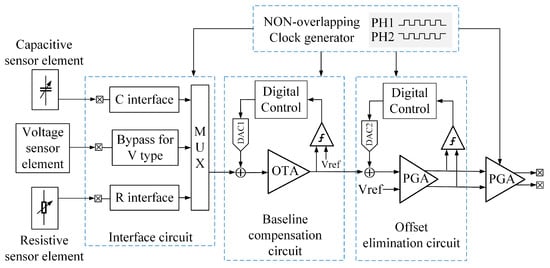
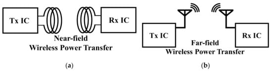
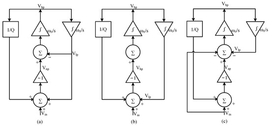
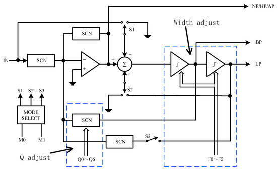
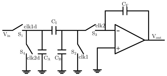
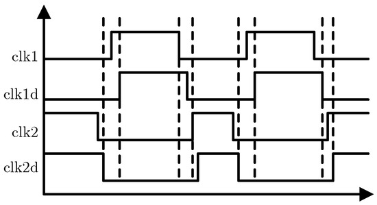
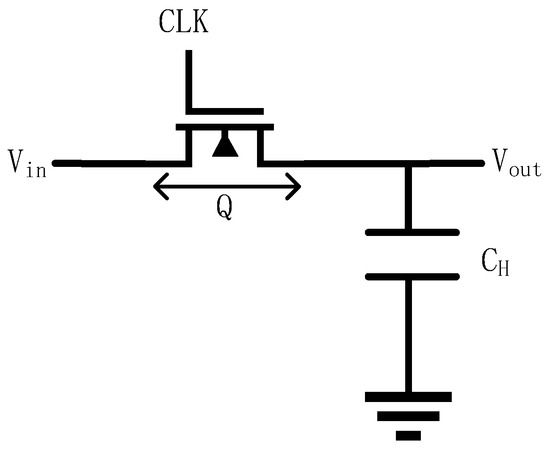
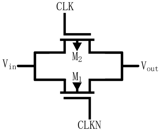
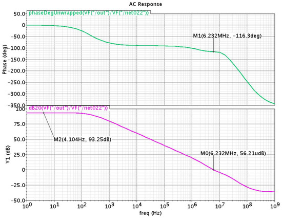
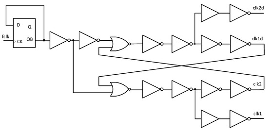
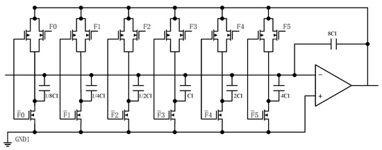
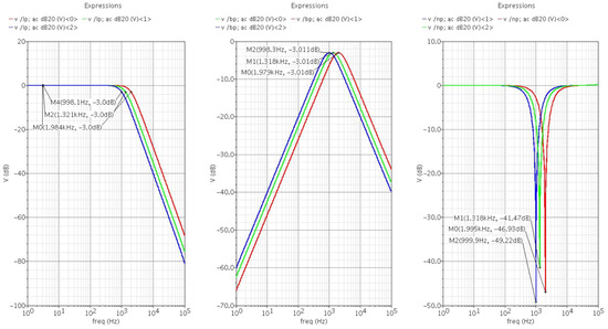
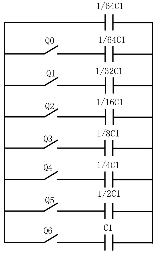
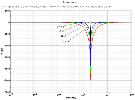
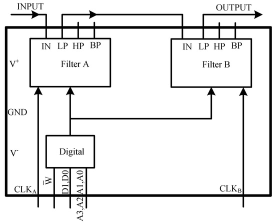
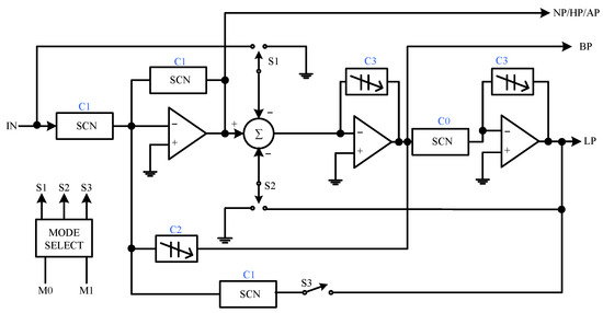
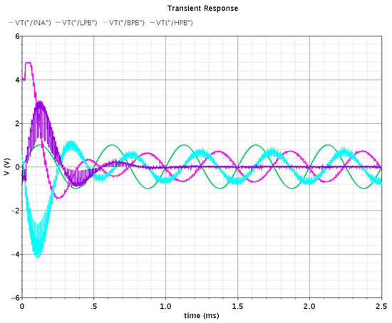
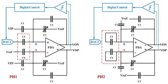
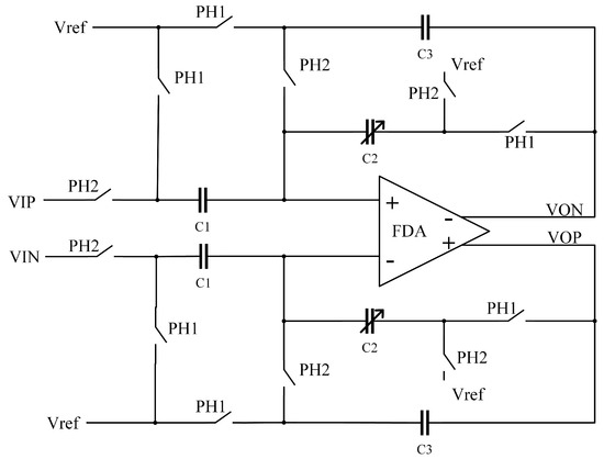
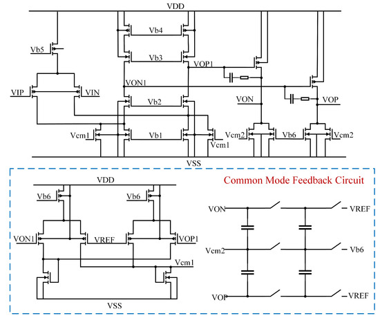
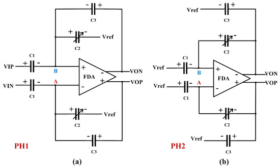
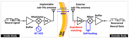
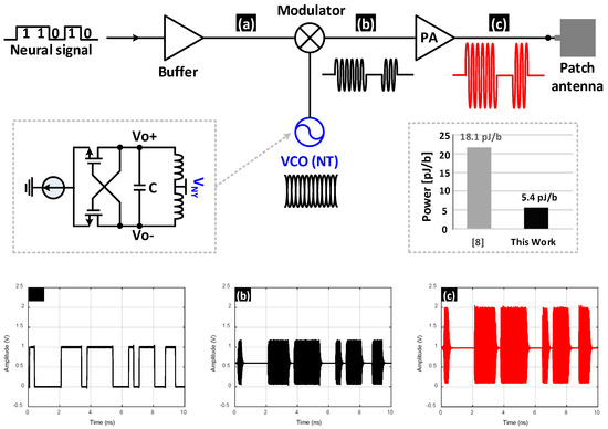
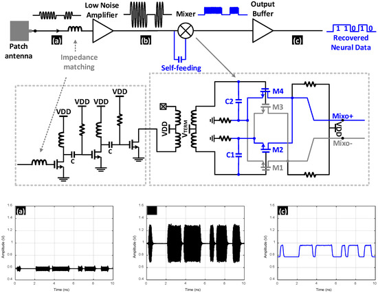
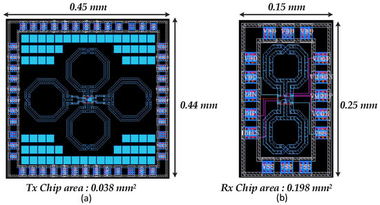
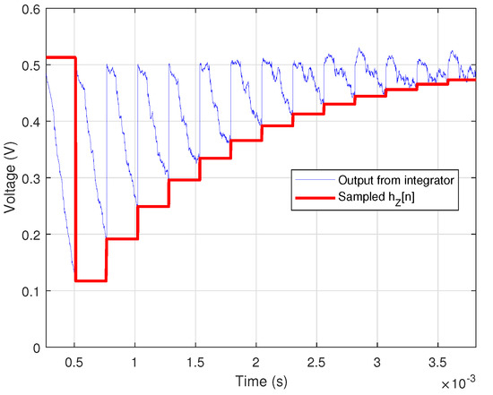
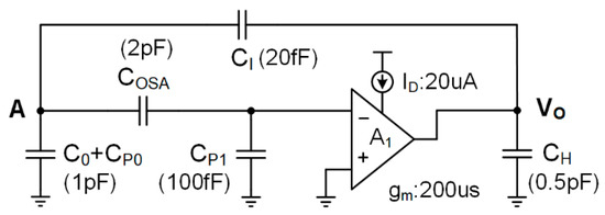
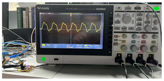
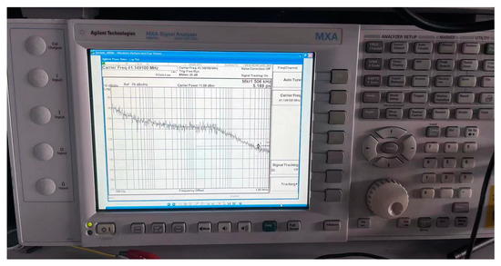
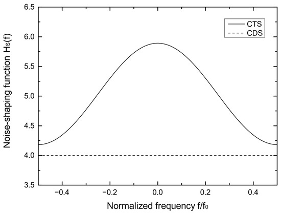
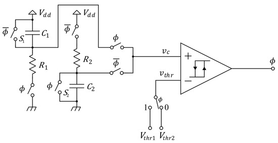
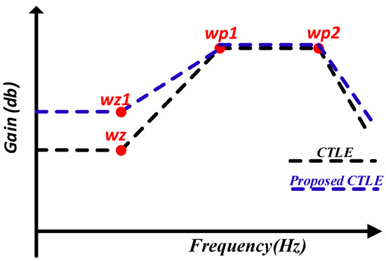
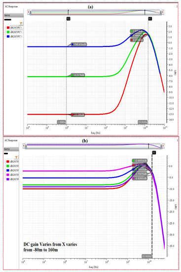
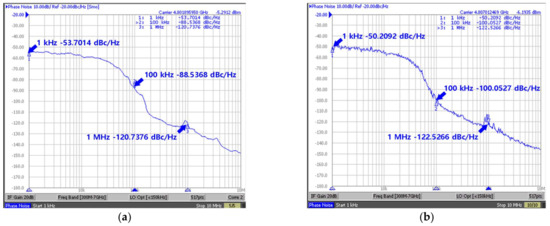
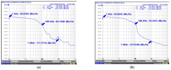
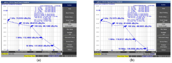
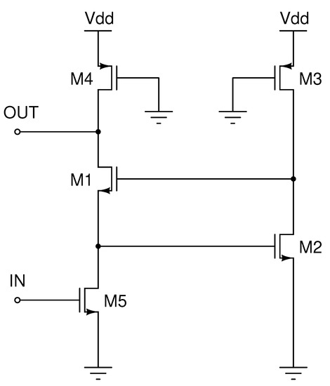
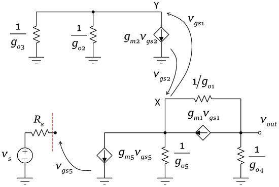
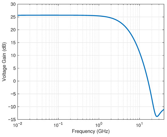
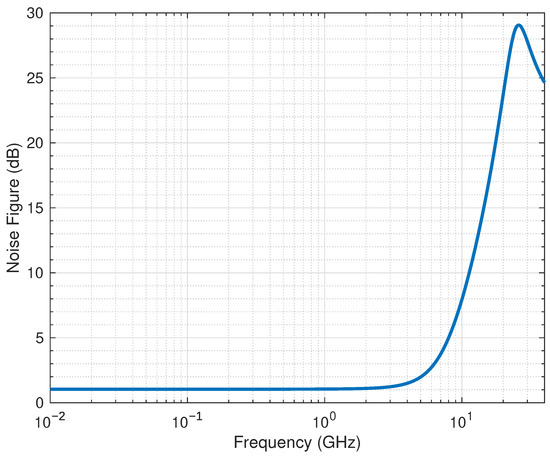
This article proposes a second-order switch-capacitor filter that integrates low-pass, high-pass, band-pass, band-stop, and all-pass, and achieves flexible bandwidth adjustment of the filter through clock rate and capacitance ratio. The final filter design consists of two completely independent second-order switch-capacitor filter channels, and
[...] Read more.
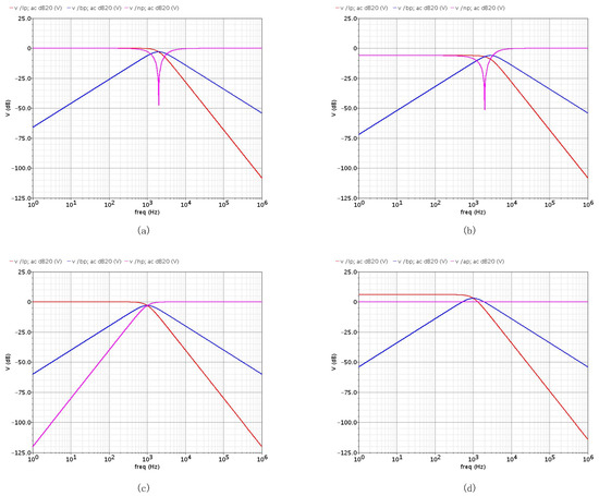
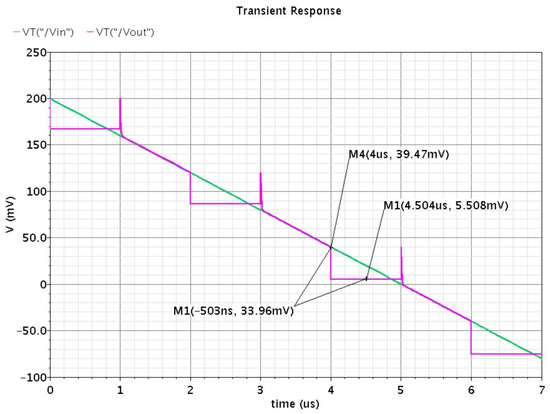
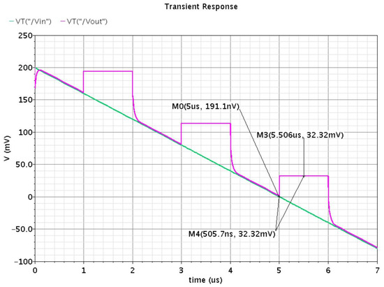
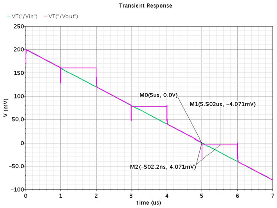
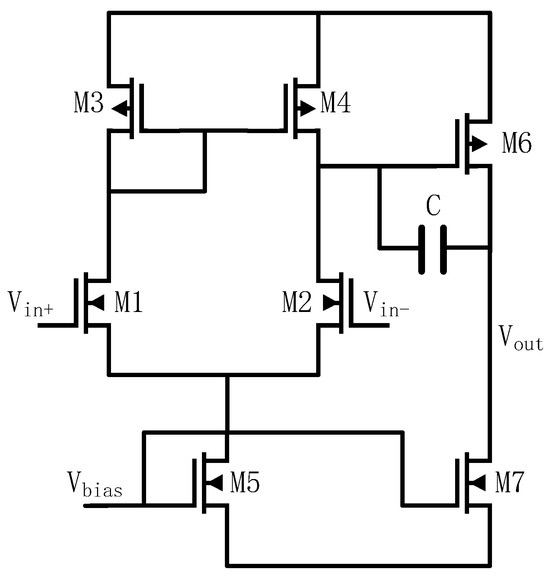
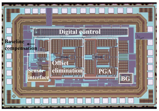
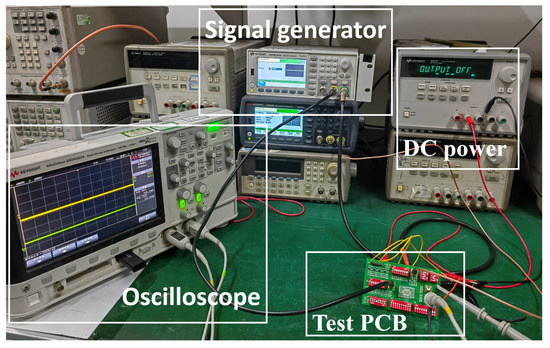
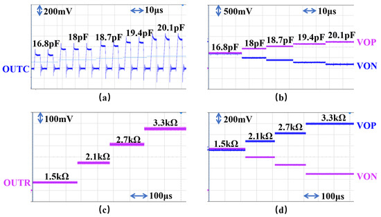
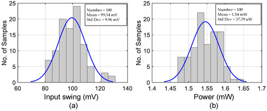
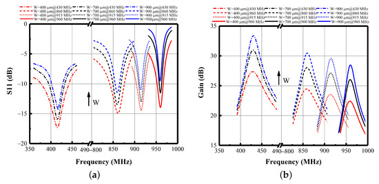
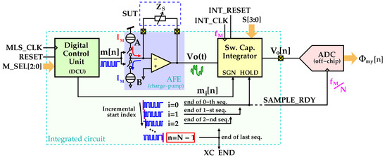
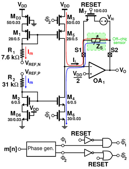
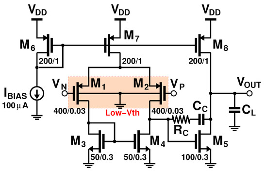
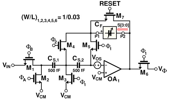
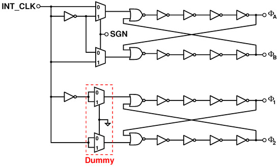
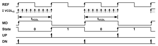
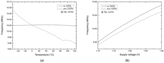
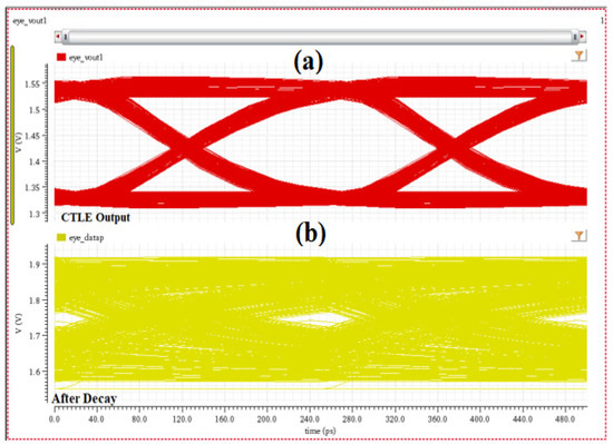
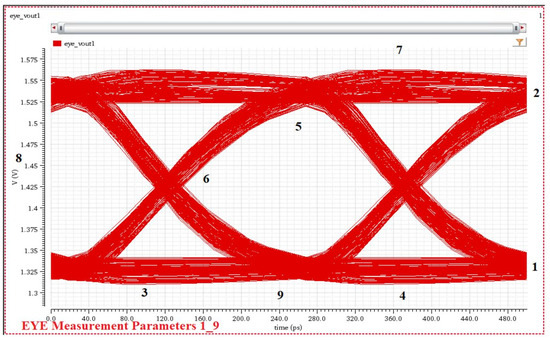
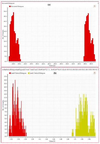
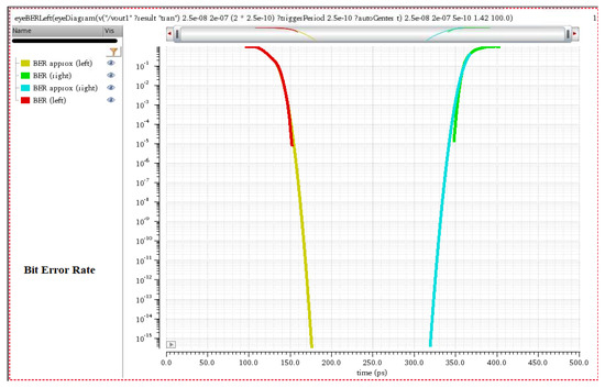
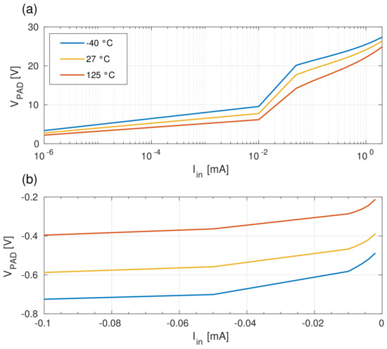
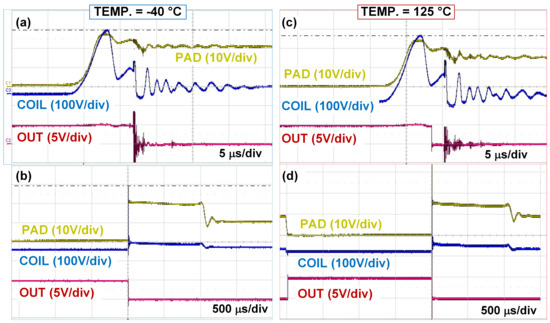
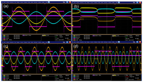
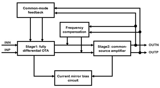
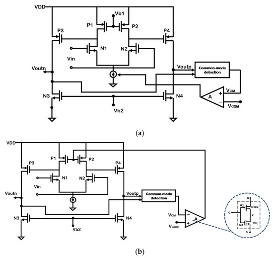
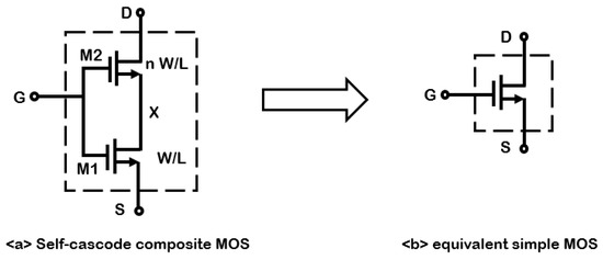
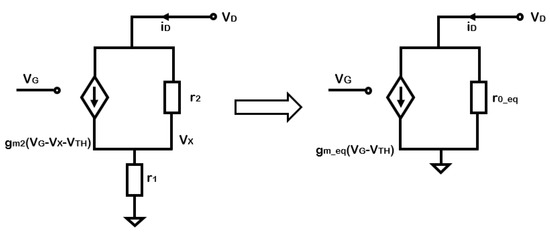
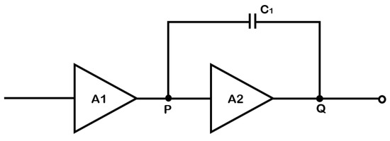
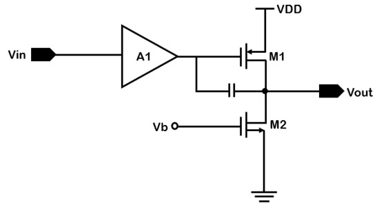
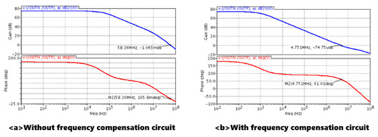
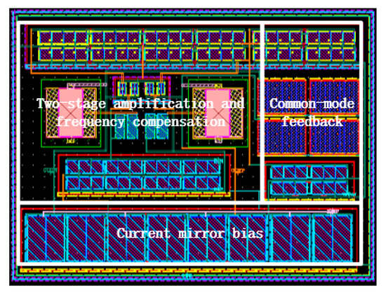
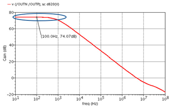
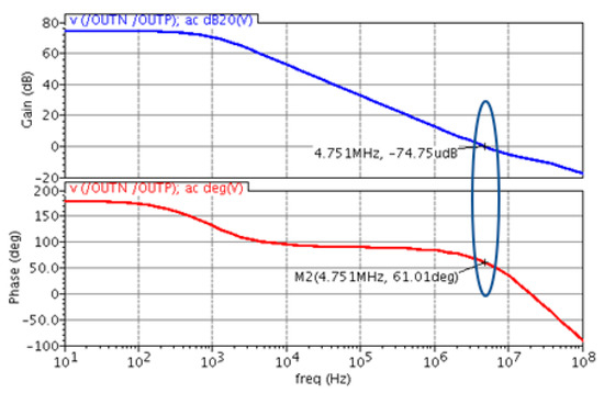
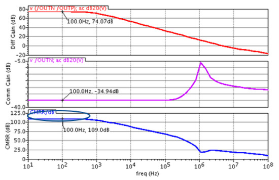
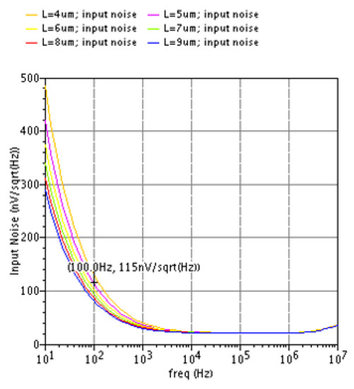
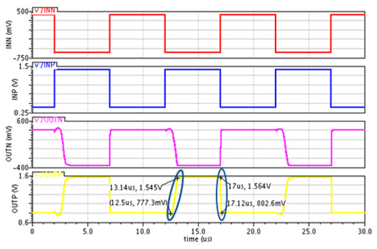
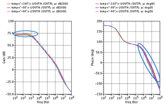
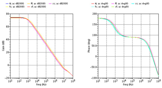
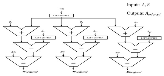
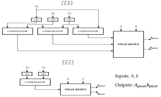
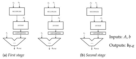
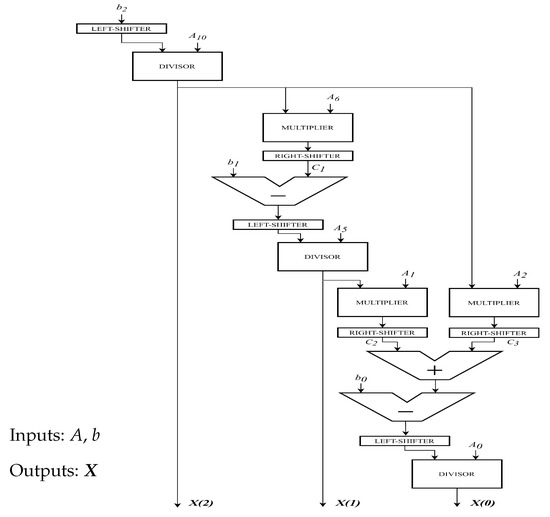
This article proposes a second-order switch-capacitor filter that integrates low-pass, high-pass, band-pass, band-stop, and all-pass, and achieves flexible bandwidth adjustment of the filter through clock rate and capacitance ratio. The final filter design consists of two completely independent second-order switch-capacitor filter channels, and a 4-order Butterworth low-pass filter is designed through two-stage cascades. The two completely independent second-order switch-capacitor filters are integrated on a single chip and manufactured using the Huahong BCD350GE high-voltage 24 V process. The measurement results indicate that the proposed switch-capacitor filter achieves various functional filtering characteristics and achieves a bandwidth of 5 Hz to 10 kHz. The chip area is 5.1 × 3.1 mm
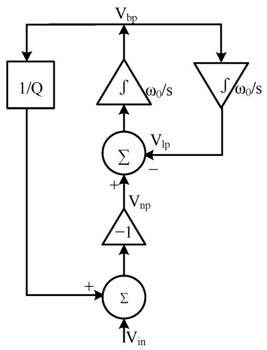
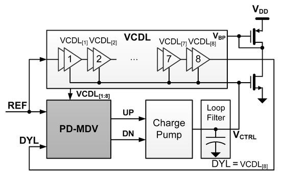
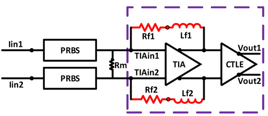
Figure 1
