


Coatings 2022, 12(3), 293; https://doi.org/10.3390/coatings12030293 - 22 Feb 2022
Cited by 8 | Viewed by 2588
Abstract
►
Show Figures
Active semiconductor layers of TiO2 were synthesized via pulsed laser deposition in He, N2, O2, or Ar to manufacture DSSC structures. As-prepared nanostructured TiO2 coatings grown on FTO were photosensitized by the natural absorption of the N719
[...] Read more.
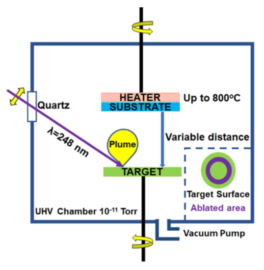
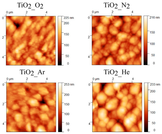
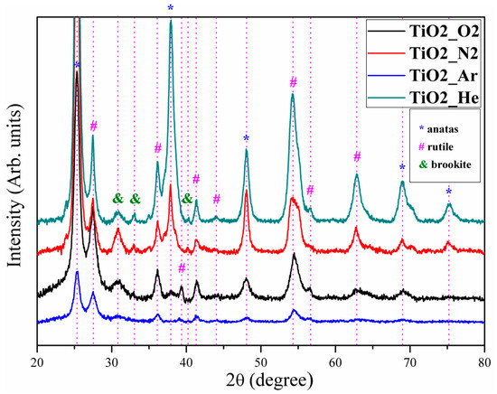
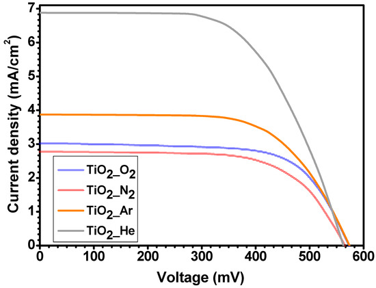
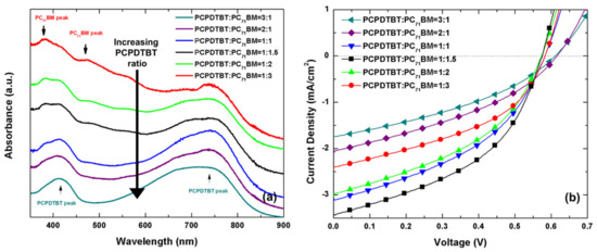
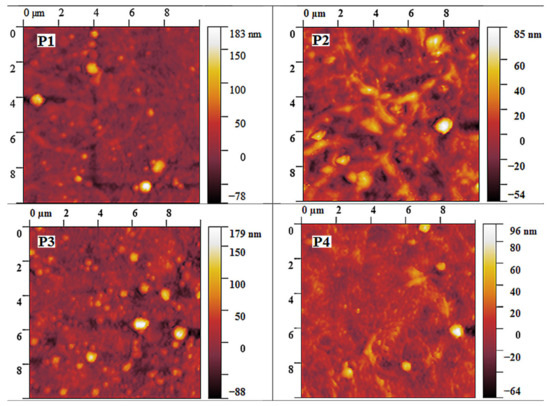
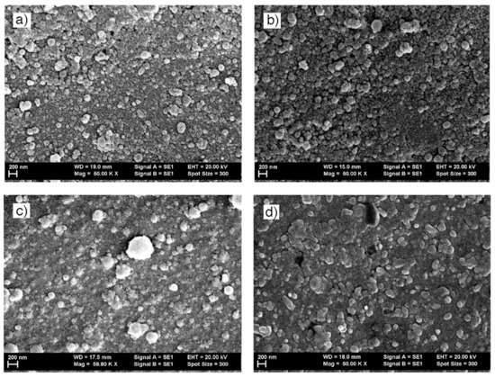
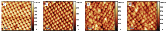
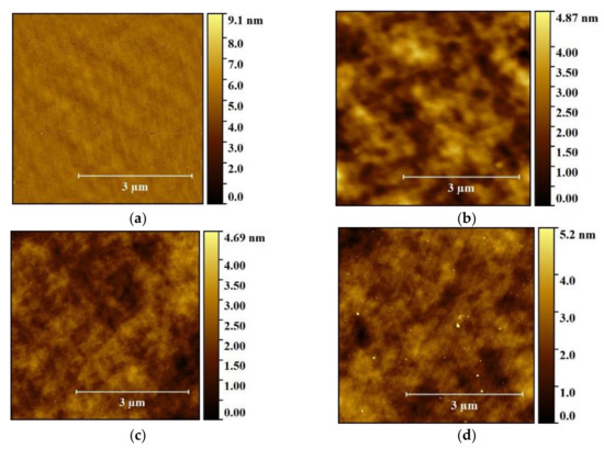
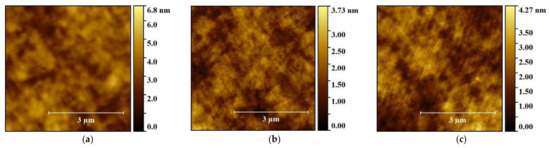
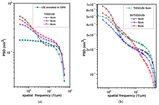
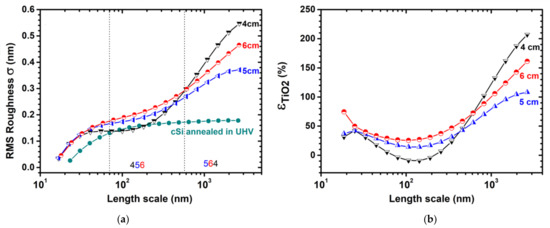
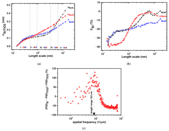
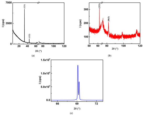
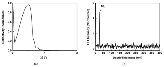
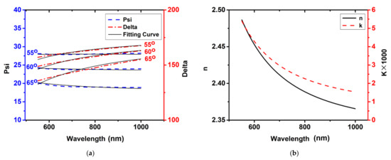
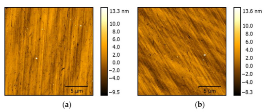
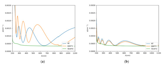
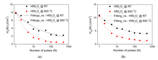
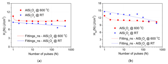
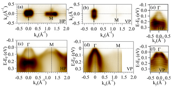
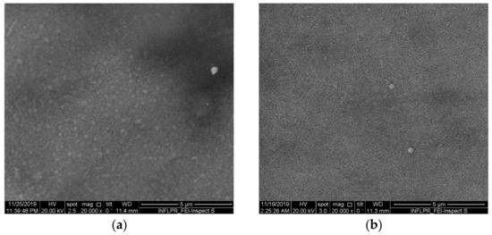
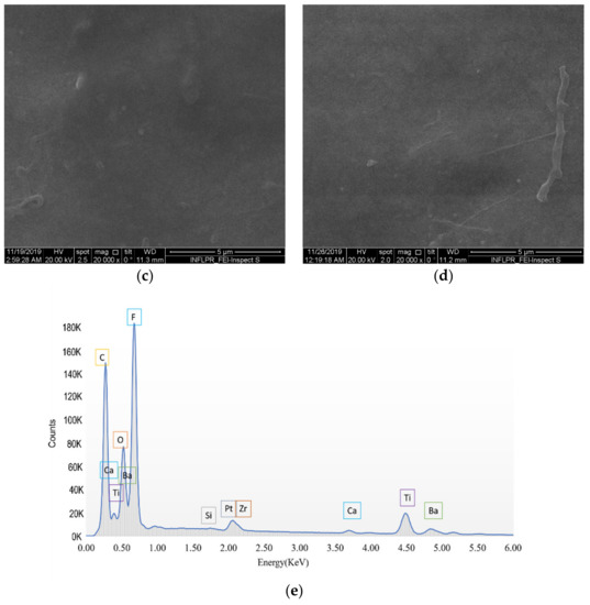
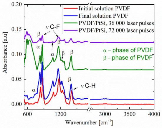
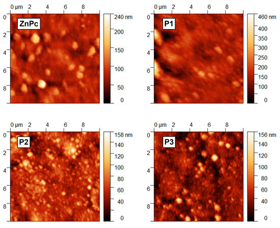
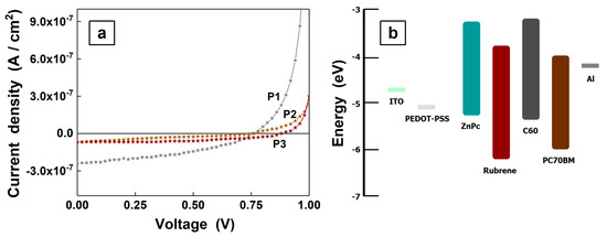
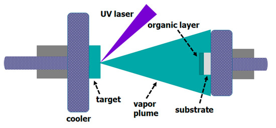
Active semiconductor layers of TiO2 were synthesized via pulsed laser deposition in He, N2, O2, or Ar to manufacture DSSC structures. As-prepared nanostructured TiO2 coatings grown on FTO were photosensitized by the natural absorption of the N719 (Ruthenium 535-bis TBA) dye to fabricate photovoltaic structures. TiO2 photoanode nanostructures with increased adsorption areas of the photosensitizer (a combination with voluminous media) were grown under different deposition conditions. Systematic SEM, AFM, and XRD investigations were carried out to study the morphological and structural characteristics of the TiO2 nanostructures. It was shown that the gas nature acts as a key parameter of the architecture and the overall performance of the deposited films. The best electro-optical performance was reached for photovoltaic structures based on TiO2 coatings grown in He, as was demonstrated by the short-circuit current (Isc) of 5.40 mA, which corresponds to the higher recorded roughness (of 44 ± 2.9 nm RMS). The higher roughness is thus reflected in a more efficient and deeper penetration of the dye inside the nanostructured TiO2 coatings. The photovoltaic conversion efficiency (η) was 1.18 and 2.32% for the DSSCs when the TiO2 coatings were deposited in O2 and He, respectively. The results point to a direct correlation between the electro-optical performance of the prepared PV cells, the morphology of the TiO2 deposited layers, and the crystallinity features, respectively.
Full article
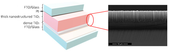
Figure 1