
Bandpass Sigma–Delta Modulation: The Path toward RF-to-Digital Conversion in Software-Defined Radio


Instituto de Microelectrónica de Sevilla, IMSE-CNM (CSIC/Universidad de Sevilla), C/Américo Vespucio 28, 41092 Sevilla, Spain
Chips 2023, 2(1), 44-69; https://doi.org/10.3390/chips2010004
Submission received: 11 December 2022
/
Revised: 15 February 2023
/
Accepted: 24 February 2023
/
Published: 2 March 2023
Abstract
:This paper reviews the state of the art on bandpass modulators (BP-Ms) intended to digitize radio frequency (RF) signals. A priori, this is the most direct way to implement software-defined radio (SDR) systems since the analog/digital interface is placed closer to the antenna, thus reducing the analog circuitry and doing most of the signal processing in the digital domain. In spite of their higher programmability and scalability, RF BP-M analog-to-digital converters (ADCs) require more energy to operate in the GHz range as compared with their low-pass (LP) counterparts. This makes conventional direct conversion receivers (DCRs) the commonplace approach due to their overall smaller energy consumption. This paper surveys some circuits and systems techniques which can make RF ADCs and SDR-based transceivers more efficient and feasible to be embedded in mobile terminals.
1. Introduction
The micro/nanoelectronics industry has exponentially grown over the last six decades according to Moore’s law, yielding to the integration of dozen of billions of transistors with dimensions closer to a few atoms of silicon. Among other benefits, high levels of integration allow to embed more and more functionalities onto a single chip, including sensing interfaces, communication systems, memory and computing, among others. In addition to the reduced cost, technology downscaling has pervasively miniaturized the electronic devices, going from multi-chip components connected in printed circuit boards (PCBs) to chip sets encapsulated in system-in-packages (SiPs) to monolithic system-on-chip (SoC) solutions. This pervasive miniaturization is making it possible for electronic devices and their derived technologies—such as artificial intelligence (AI), big data, robotics, Internet of Things (IoT), etc.—to be more and more present in our daily lives [1,2,3]. These technologies are accelerating their pace of penetration, transforming many of our social and economic activities from a physical to virtual format. Indeed, our natural environment is being surrounded with a set of digital layers, which allows us to iterate with virtual entities and objects in an augmented reality—also referred to as the metaverse [4].
Communication systems are essential parts of IoT nodes and end terminals. In the majority of cases, information is transmitted wirelessly over radio frequency (RF) bands of the electromagnetic spectrum, i.e., carried out by analog signals. This requires an important portion of wireless transceivers to perform their functions in the analog/RF domain to adapt and transform signals from/to the digital domain, where they are processed by the digital signal processor (DSP). Unfortunately, analog components do not scale as digital parts do. Indeed, deep nanometer mainstream CMOS technologies are more suited to integrate fast digital transistors rather than accurate analog circuits. This is one of the main reasons why every time a new communication protocol is developed, it usually requires dedicated RF chip sets. As a consequence, the celerity with which new functionalities are incorporated in i-devices exceeds the rate of package reduction, and the trend from multi-chip to SiPs and SoCs is still a technological challenge in reaching the requested quality standards while keeping the form factor, cost and time-to-market deployment reduced [5,6,7,8,9,10].
Addressing this challenge implies redefining the concept of mobile terminals, going from pure hardware-based to hybrid hardware/software-based devices. As envisaged by Mitola in 1995 [11], a software-defined radio (SDR) is defined as a universal radio platform which can be programmed to steer any frequency band, and process arbitrary communication protocols, while ensuring the required quality of service as well as guaranteeing privacy and security [6]. An ideal SDR transceiver—conceptually depicted in Figure 1a—would process all information in the digital domain so that it would be composed by three main building blocks: the antenna, the A/D interfaces and the DSP. This way, most parts of the hardware in this ideal SDR system are digital, thus benefiting from technology downscaling and a higher programmability to new standards and applications. Unfortunately, this implementation is not realistic due to the huge amount of power consumed by the A/D interfaces—the analog-to-digital converter (ADC) in the receiver and the digital-to-analog converter (DAC) in the transmitter—which requires at least some analog/RF signal conditioning circuitry to implement an efficient interface between RF signals and the digital data, depicted in Figure 1b.
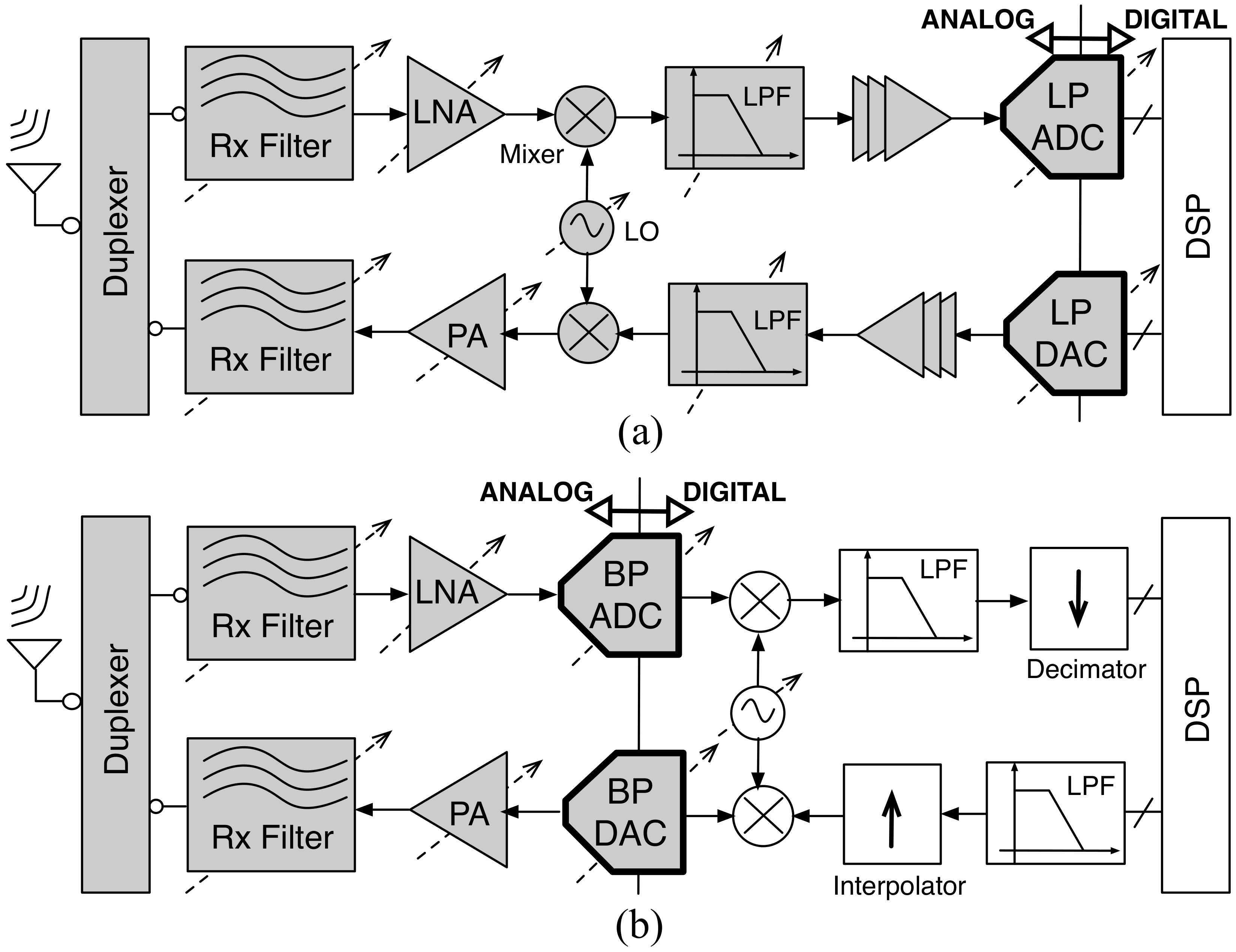
The analog/RF-to-digital interface of multi-mode/multi-standard SDR transceivers can be implemented in two ways as depicted in Figure 2. In both cases, all building blocks need to be reconfigurable/programmable in order to adapt their performance to the required specifications. The approach in Figure 2a, known as direct conversion transceiver (DCT), translates the analog/RF signal from/to the RF domain to the baseband by means of an analog downconverter (in the receiver side) and an upconverter (in the transmitter side). This way, an LP ADC can be used to digitize downconverted signals in the receiver. Analogously, an LP DAC transforms the baseband digital data before being upconverted to RF in the transmitter. By contrast, the approach in Figure 2b requires to implement the analog/digital interfaces in the RF domain, i.e., an RF ADC in the receiver and an RF DAC in the transmitter. The main benefit of this approach is the reduced analog content, and hence, it is less sensitive to analog circuit impairments due to I/Q down-mixing, flicker noise and DC offset. However, the price to pay is that the RF/digital interface requirements are more demanding, with the subsequent penalty in the power consumption—a key factor in wireless transceivers and portable devices [12,13,14,15,16].
This paper focuses on the receiver path of SDR transceivers, considering the RF-digitization approach in Figure 2b and the ADC as one of its key building blocks. Target specifications for such an RF ADC may involve digitizing signals with an 8–12 bit effective resolution within a programmable 30 kHz–300 MHz bandwidth with a tunable carrier frequency ranging from 0.4 GHz to 6 GHz. These specifications should be fulfilled with a reduced amount of power to maximize device autonomy. Moreover, a high degree of programmability is needed in order to adapt the ADC performance to the electromagnetic environment conditions, band occupancy, number of interferences, battery status, etc. The state of the art on ADCs for wireless communications is dominated by three techniques or a combination of them, namely: Sigma–Delta modulators (Ms), noise-shaping (NS) SAR and Pipeline. Although wideband Nyquist-rate ADCs—such as SAR, Pipeline or hybrid SAR-Pipeline—are potentially more efficient than Ms for digitizing wideband signals, bandpass (BP) Ms are, a priori, a better choice for implementing an early RF digitization of the desired signal band/channel in Figure 2b, with a high degree of tunability and adaptability of its performance metrics [17].
Since their conception in 1989 [18,19], a number of BP-M ADCs have been reported to implement RF digitizers [16,20,21,22,23,24,25,26,27,28,29,30,31,32,33,34,35,36]. In spite of the promise of being the best solution for RF-to-digital conversion, performance metrics of BP-Ms are less efficient than their low-pass (LP) counterparts. The reasons behind this will be analyzed in this paper through a review of the state of the art. The main BP-M architectures and circuit techniques will be overviewed and compared in terms of their main performance metrics, namely, effective resolution, operating frequency, and power dissipation. Cutting-edge circuits and systems will be identified to help designers select the most suited BP-M topology and circuit technique according to their target specifications.
Following this introduction, the paper is organized as follows. Section 2 revisits the fundamentals and basic concepts of BP-Ms, putting emphasis on the discrete-time (DT) implementations. Section 3 overviews continuous-time (CT) BP-Ms, focusing on their use in RF ADCs in SDR receivers. Section 4 analyzes the state of the art on BP-Ms and compares their performance metrics with Ms and other kinds of ADCs. Emerging circuits and systems techniques are identified as potential game changers to digitize RF signals in SDR systems. Finally, conclusions are drawn in Section 5.
2. Bandpass Modulators: Fundamentals and Basic Concepts
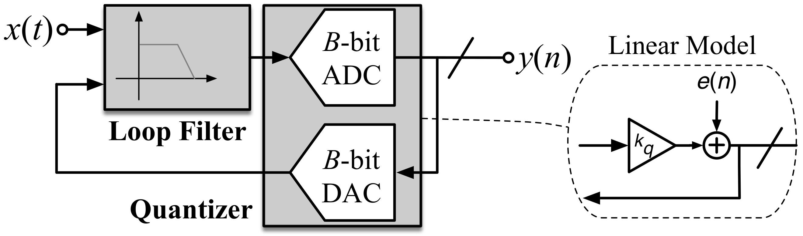
Figure 3 shows the conceptual block diagram of a M, which consists of a loop filter and a B-bit quantizer connected in a feedback loop [37]. Assuming a linear additive white noise model for the quantizer as depicted in Figure 3, the Z-transform of the M output, y, can be written as follows.
where STF and NTF stand for the signal- and noise-transfer functions, respectively, given by
with being the gain of the quantizer and being the transfer function of the loop filter. Considering an Lth-order loop filter, the dynamic range (DR) of a M can be approximately written as
where stands for the oversampling ratio, is the sampling frequency, and is the signal bandwidth. The effective number of bits (ENOB) of a M can be obtained from Equation (3) as
Hence, Ms increase ENOB with OSR by approximately dB/octave—second term in (3). The three key parameters, namely OSR, L and B, define the system-level performance of Ms, and can be combined in many ways, giving rise to a huge number of Ms—LP or BP; single-loop or cascade; single-bit or multi-bit; continuous-time (CT) or switched-capacitor (SC)—in order to achieve the maximum DR. In the case of BP-Ms—the object of this paper—the zeroes of the NTF are placed around an arbitrary frequency, usually referred to as the notch frequency, . This frequency corresponds to the carrier frequency of incoming signals in RF receivers as illustrated in Figure 4. The quantization noise is reduced only in a narrow band () around , thus taking advantage of a high OSR to meet the required DR according to Equation (3) [37].
2.1. Quantization Noise Shaping in BP-Ms
BP-Ms can be implemented using either discrete-time (DT)—basically switched capacitor (SC)—or CT circuit techniques. The latter are mostly used in RF ADCs due to their higher operating frequencies—in the GHz range. Moreover, CT circuits merge better with other circuits of the SDR receiver and implement some RF functions, such as out-of-band blocker, image-rejection filtering, anti-aliasing, etc. [38]. However, as will be discussed later in this paper, CT BP-Ms are usually synthesized from their equivalent DT counterparts. In the analysis that follows, a DT realization is assumed without loss of generality.
In the more general case, the loop-filter of BP-Ms is a 2Lth-order BP filter composed of resonators—or biquad sections—with a transfer function given by [39]:
where denotes the numerator polynomial and and stand for conjugate-complex poles of . Replacing Equation (5) in Equation (2) and assuming , it can be shown that the NTF of BP-Ms can be expressed as
which has L zeros placed at and . Assuming that , with being the sampling period, and considering that is designed so that the denominator in Equation (6) is unity, the NTF of an 2Lth-order BP-M can be written as
Note that NTF has its zeroes placed on the Z-domain unit circle at complex-conjugate and , i.e., and . This means that a th-order BP-M has L zeroes placed at the signal band, thus being equivalent to an Lth-order LP-M. As illustrated in the simulations shown in Figure 5, the notch frequency, , can be programmed in order to make BP-Ms tunable within the Nyquist band, i.e., from DC to . As will be discussed later, this feature is applied in wireless transceivers to increase the programmability of RF digitizers by reducing the quantization noise around the desired signal channel.
The power spectral density (PSD) of the quantization noise shaped by BP-Ms can be calculated as
where is the quantization step, defined as , with being the full-scale (FS) range of the quantizer.
The quantization in-band noise power, , can be computed by integrating in the signal bandwidth as
Knowing that , it can be shown that in the case of BP-Ms, DR is given by [39]
Note that the above expression is equal to (3) if . This notch location is the most common case as discussed below.
2.2. Notch Frequency Location and Basic Architectures
One of the most common choices for the notch frequency is since this passband location optimizes the trade-off between anti-aliasing filtering and image-rejection filtering in wireless transceivers based on BP-Ms as that shown in Figure 2 [39]. The digital downconverter in Figure 2 can be notably simplified since the (digital) local oscillator (LO) signal is designed such that it generates a digital sinewave as
which is a data series of s, 0 s, and s, easily implemented by simple digital logic. This makes it easier and simple the gate-level implementation of the digital mixer and the numerical controlled oscillator (NCO) in Figure 2. More importantly, assuming in (7), the NTF of a 2L-th order BP-M yields
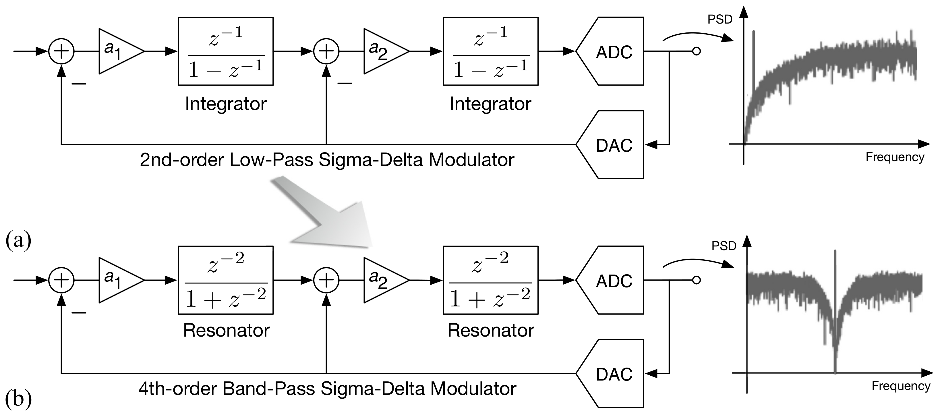
which can be derived by applying a transformation to the NTF of a Lth-order low-pass (LP) M, given by [37]. This way, any arbitrary BP-M can be derived from an initial LP-M by applying this Z-domain transformation. Figure 6 illustrates this transformation applied to a 2nd-order LP-M, which becomes a 4th-order BP-M, and loop-filter integrators are transformed into resonators.
The transformation also allows to place the input signal at [40] instead of given that the spectrum is symmetrical with respect to . Making preserves the requirements of the anti-aliasing filter compared to the case, but the image-rejection filter specifications can be relaxed. In addition, it allows for either the clock rate to be reduced to or the signal processing to be three times faster. However, the OSR is also reduced by a factor of three with the subsequent penalty in DR loss.
Placing the signal band around also has some disadvantages. On the one hand, in the presence of nonlinearities of the analog circuitry of the M, any intermodulation distortion products resulting from the mixing of tones at with the input signal will fall inside the modulator passband and will thus corrupt the signal information. On the other, for a given RF input, the clock rate demands are more restrictive than placing between and . For instance, those wireless standards—such as some IEEE 802.11 standard—operating in the frequency band of 5 GHz would require a sampling frequency of 20 GHz, with the subsequent penalty in power dissipation [41].
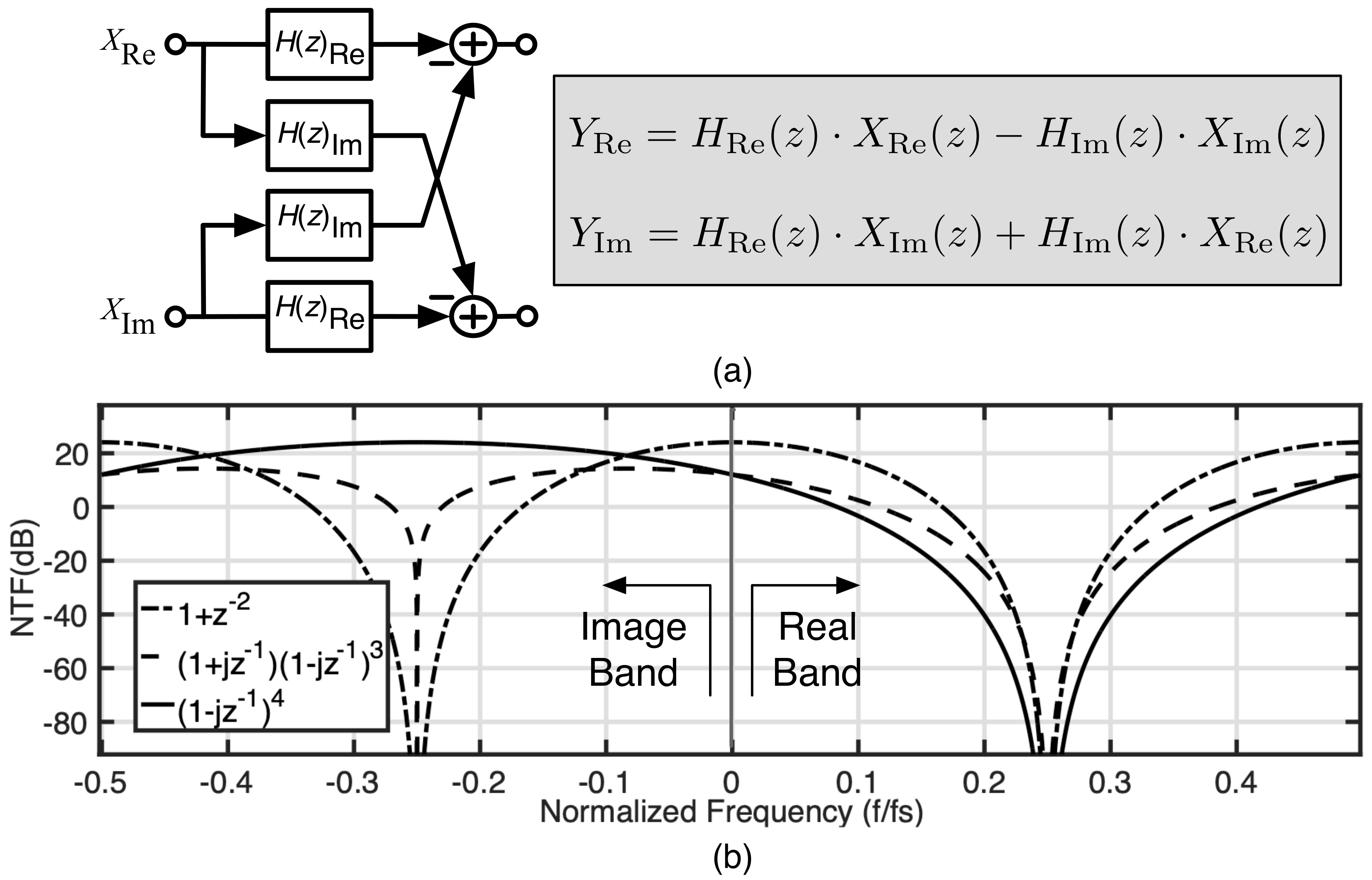
Although placing the notch frequency at is the most common approach, other alternative approaches have been reported to synthesize BP-Ms and allocate the zeroes of the NTF. Some techniques are based on the use of complex BP filters in quadrature architectures [42,43] as illustrated in Figure 7a. The resulting NTF has complex zeroes that are not necessarily conditioned to be placed symmetrically around DC. This allows an L-th order BP- to place L zeroes at without having any zero at . The solution is more energy efficient than conventional approaches since no power is dedicated to digitizing the negative (imaginary) frequency bands [44]. One of the main limitations of this approach is the mismatch between both real and imaginary paths, which causes signal image components to appear in the signal band, thus corrupting the information. This problem can be mitigated by placing some zeroes in the imaginary band—as illustrated in Figure 7b. However, this reduces the ratio between the number of NTF zeroes and the filter order—one of the main benefits of quadrature BP-Ms.
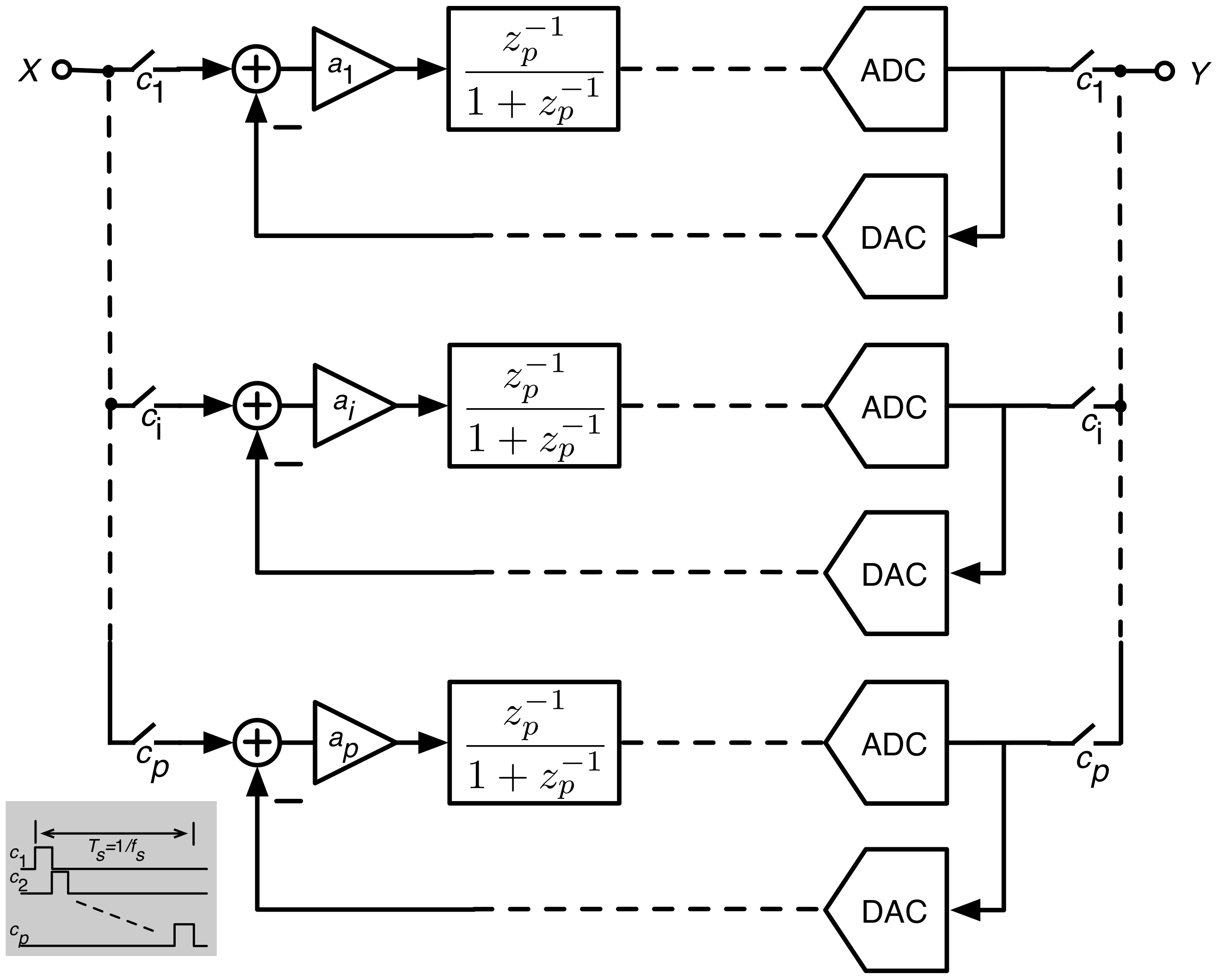
Another alternative to reduce the clock rate as compared to the approach is based on time-interleaved (TI) or P-path loop filters [45]. The idea of TI BP-M consists of splitting a modulator clocked at in several TI BP-M paths, each one operating at , with P being the number of paths, as illustrated in Figure 8. Similar to quadrature BP-Ms, TI BP-Ms are also limited by circuit impairments, such as offset, gain and timing mismatch, which causes spur tones to appear at the output spectrum, thus degrading the noise shaping [46].
Based on a similar idea, some authors proposed a polyphase decomposition of the NTF of BP-Ms [47] as follows:
where stands for transfer functions of the j-th path BP-M. For instance, let us assume a 2nd-order polyphase BP-M with and a NTF with zeros at , given by
In this case, the polyphase () decomposition leads to and , where is a coefficient that changes the zeroes of NTF from to , when it varies from to . Assuming that , we obtain the expression of NTF given in Equation (7). It can be shown that the spur tones due to path mismatches fall out of the signal band at , with P being the number of paths used in the polyphase decomposition [47].
3. Continuous-Time BP-Ms
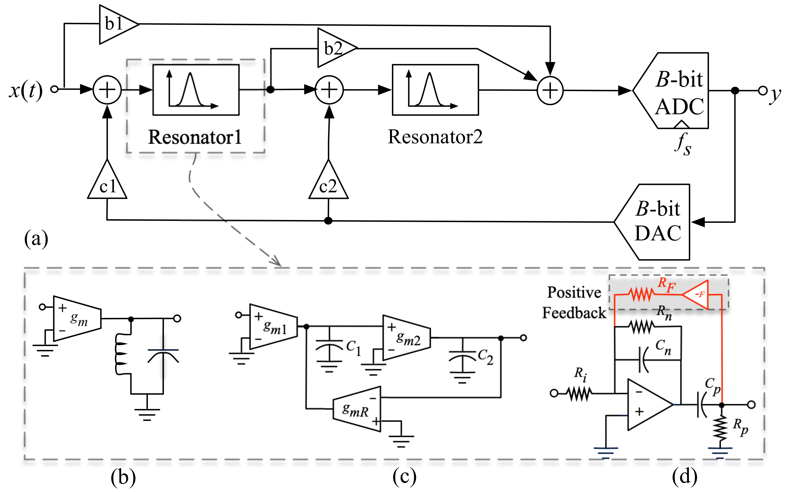
The BP-Ms described above assume a DT (usually SC) realization of the loop filter. However, CT BP-Ms are more suited to digitize RF signals since GHz-range sampling rates are needed. CT loop filters can operate at higher frequencies than their SC counterparts, while consuming less power and implement an inherent anti-aliasing filtering. The loop-filter of CT BP-Ms can be realized using either active (RC or Gm-C) resonators or passive LC resonators as conceptually depicted in Figure 9. RF BP-Ms have two main design challenges. The first is to achieve a high-quality and accurate resonance frequency. The second is to target a wide tuning range of the carrier (or notch) frequency. LC tanks are a good approach from a power and linearity perspective, although they typically support only an octave of range, whereas active-(Gm-C/RC) resonators can be widely tunable but require amplifiers with strong requirements—high DC gain and gain bandwidth (GB) [48]. Single op amp resonators are a good alternative to reduce power consumption. Some authors propose the use of positive feedback—implemented by a passive RC network—to enhance the quality factor of resonators. Figure 9d illustrates this approach proposed by Chae et al. [49].
Regardless of the circuit technique used to implement CT BP-Ms, it is difficult to keep the required specifications within a wide tuning range. For that reason, it is usual to set the notch frequency constant, usually located at . For the analysis that follows, this approach will be considered and the problem of tuning will be discussed later.
3.1. LC-Based CT BP-M Architectures
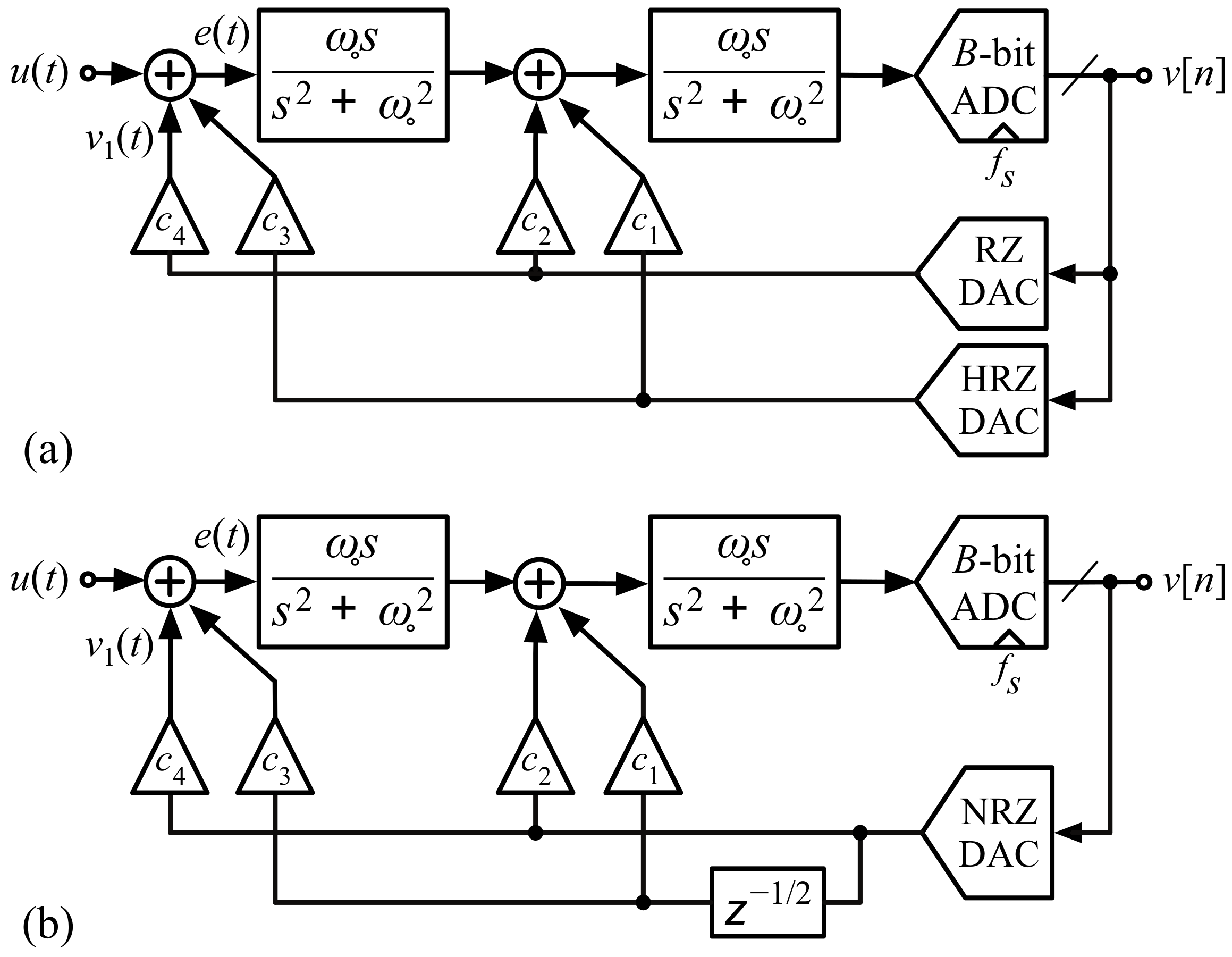
Figure 10 shows the block diagram of the two common approaches to implement CT BP-Ms with multi-path feedback, based on ideal (LC) resonators with a transfer function, . Normalized values of s and are considered with respect to so that (with f standing for the frequency variable) and . A 4th-order loop filter made up of two resonators with is considered. The feedback loop is implemented in two main different ways. Figure 10a [50] uses two different DAC pulse shapes, return-to-zero (RZ) and half-delay return-to-zero (HRZ), while Figure 10b [51] includes a non-return-to-zero (NRZ) DAC with different delay for each path. For the sake of simplicity, the excess loop delay (ELD) compensation path is not considered. In both cases, multiple feedback paths with their scaling coefficients are required to increase the degrees of freedom in the synthesis process, correctly restoring NTF of the DT Z-domain counterpart.
The CT BP-Ms shown in Figure 10 can be synthesized as follows. The Schreier’s toolbox [52] is used to obtain the NTF which satisfies the required specifications in terms of DR and with an out-of-band gain (OBG) (usually ), and the DT version of the loop filter transfer function can be easily derived as . The DT version of the loop-filter transfer function, , of the desired BP CT-M is therefore derived from the well-known impulse-invariant transformation as
where and denote the Z-transform and L-transform symbols, respectively, and is the transfer function of the DAC [37,53].
3.2. Widely Tunable CT BP-Ms
As stated above, one of the challenges of RF ADCs is the high sampling frequency required. Using a fixed value of (normally ), forces the variation of in order to tune the desired carrier frequency of the RF signal. For instance, if the incoming RF signal is placed at GHz, the sampling frequency should be GHz. Moreover, another important inconvenience of this approach is that a widely programmable PLL-based synthesizer is needed to vary according to the needed to place the in-coming RF signal within the passband of the modulator. For instance, if an RF ADC needs to digitize RF signals which are placed in the wireless commercial band, i.e., –6 GHz, this would require a PLL with a frequency tuning range from GHz to 24 GHz!
These limitations have motivated the interest for programmable CT BP-Ms with tunable notch frequency [24,25]. In the majority of cases, tuning range of notch frequency is limited by stability of the modulator loop filter. This problem can be circumvented if the notch frequency is taken into account as a design parameter of the BP-M. This approach, referred to as notch-aware systematic methodology [41], allows to increase the tunable notch-frequency range of LC-based BP-Ms with respect to prior art, ranging from to , while keeping their performance in terms of noise shaping, stability and sensitivity to architecture- and circuit-level nonideal effects [41].
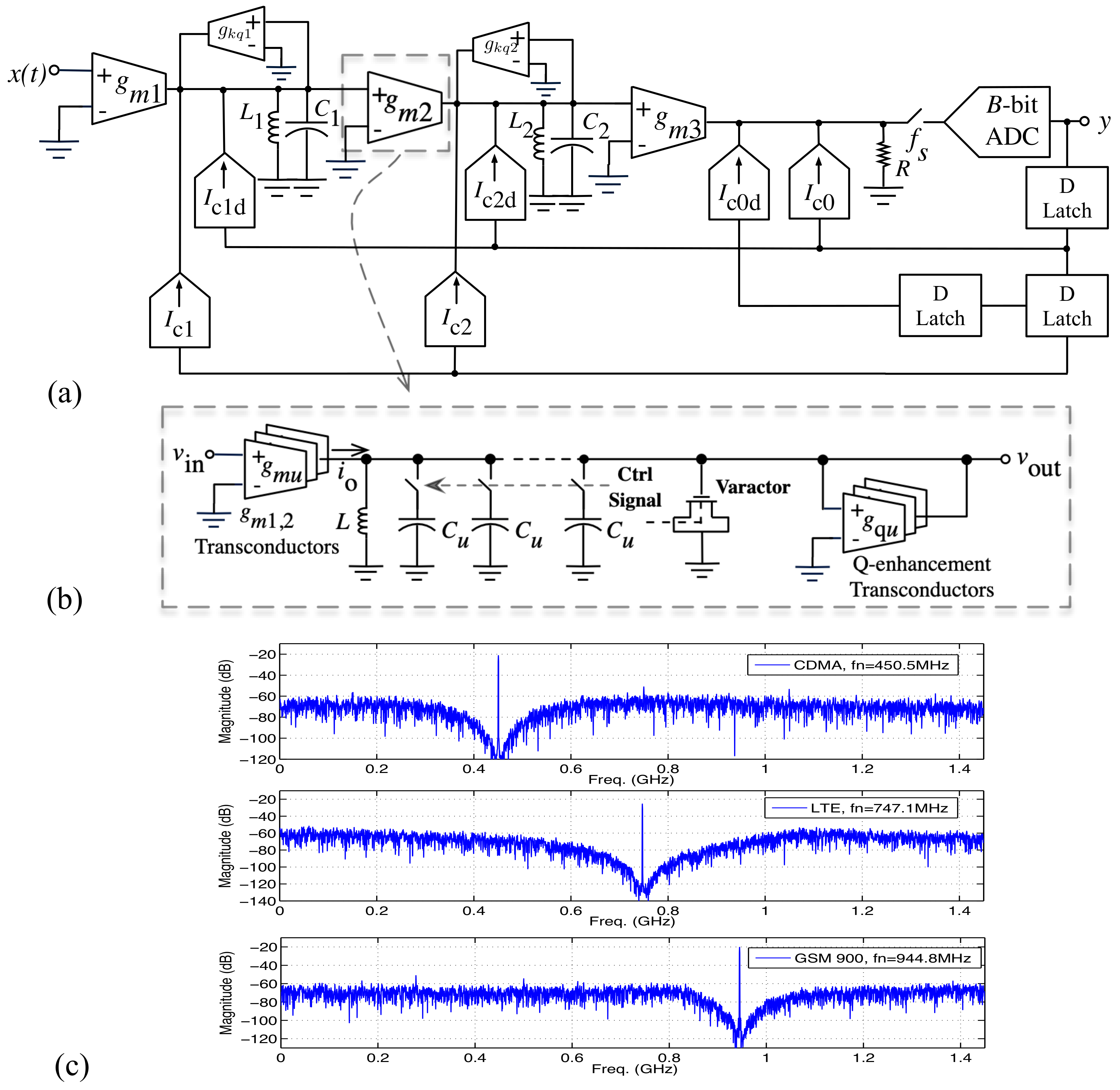
As an illustration, let us consider the Gm-LC BP-M with 4-bit quantizer shown in Figure 11. This modulator was synthesized using the notch-aware synthesis methodology. First, the Schreier toolbox is used to obtain the DT version of the NTF. The next step consists of obtaining the open-loop transfer function—from the modulator output to the input of the quantizer, computed for the different feedback branches with gain in Figure 10b as follows:
where denotes the floor operator, , and stands for the transfer function of the NRZ DAC, respectively given by
The resulted modulator loop filter can be implemented using Gm-LC resonators as shown in Figure 11a. This circuit implementation increases the programmability of the loop-filter coefficients, which are realized as switchable unitary transconductance elements, as illustrated in Figure 11b. It can be shown that the block diagrams in Figure 10b and Figure 11 are equivalent, if the following relationships are satisfied:
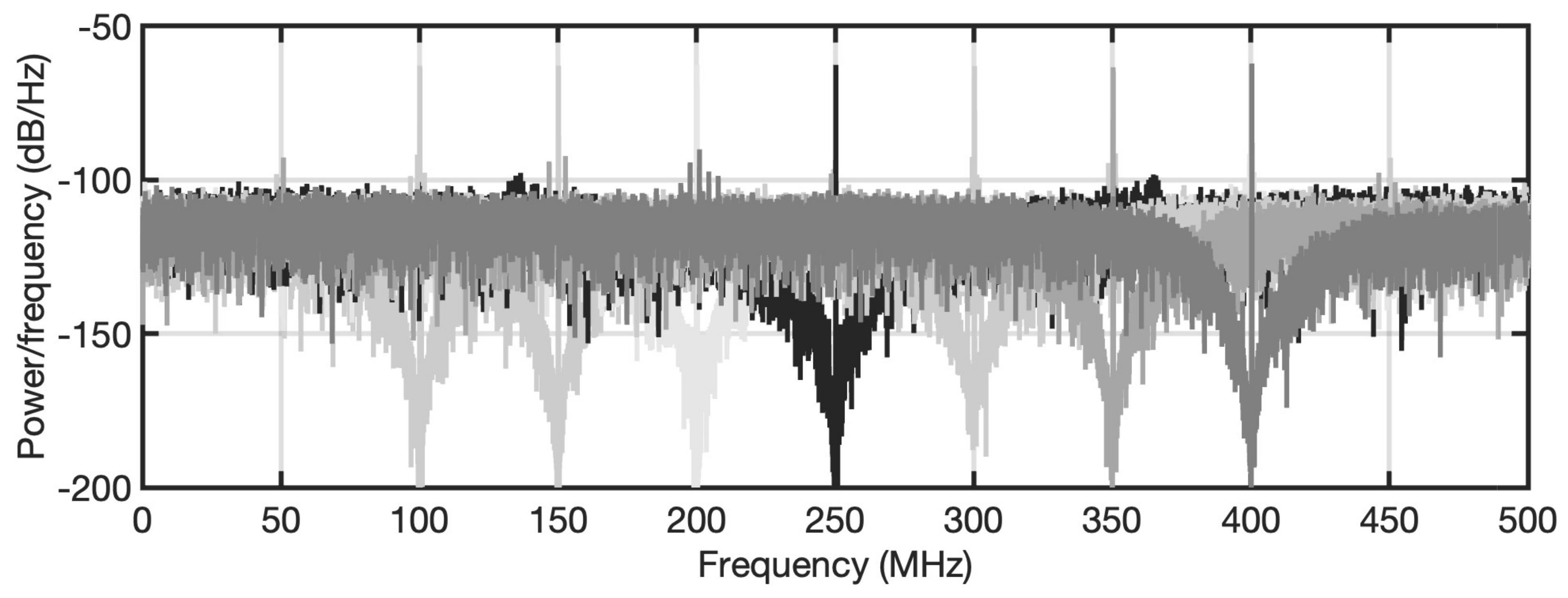
where stands for the full-scale reference voltage, and are scaling forward-path coefficients, and are the weight coefficients which scale the resonator gain, . This way, the notch frequency of the modulator can be tuned as illustrated in the simulated output spectra shown in Figure 11c.
4. State of the Art on BP-Ms
Since the first BP-M was reported in the beginning of the 1990s [55], a vast number of integrated circuits (ICs) using diverse technologies, architectures and circuit techniques have been proposed [37]. The most important specifications of any ADC are the signal bandwidth, , and the ENOB. In the case of BP-Ms, the notch frequency, , should be also considered since it would affect the amount of energy (power) needed to digitize a signal placed on it. Table 1 and Table 2 sum up the performance of the state-of-the-art BP-M ICs considered in this survey. The data analyzed in this work are collected in a spreadsheet available at http://www.imse-cnm.csic.es/~jrosa/CMOS-SDMs-Survey-IMSE-JMdelaRosa_DEC2022.xlsx.
4.1. Low-Pass vs. Bandpass Ms
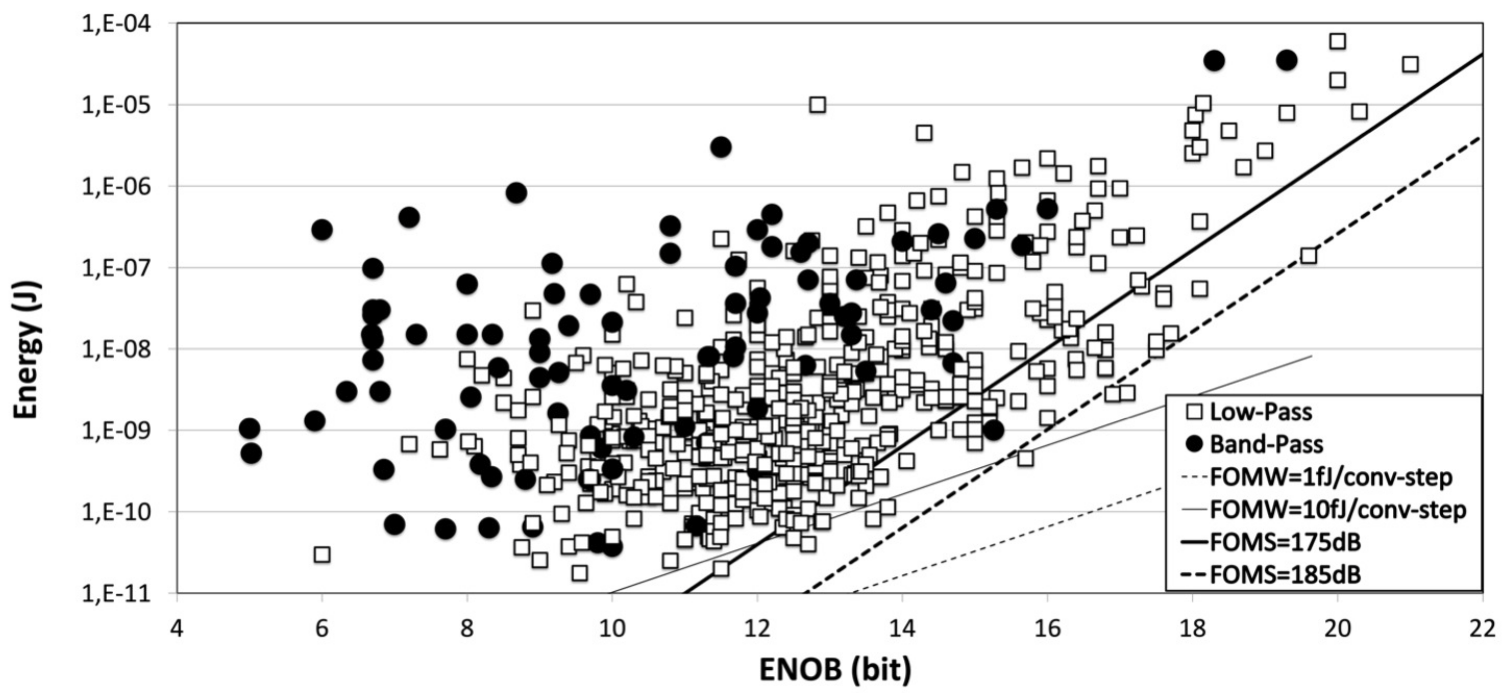
The analysis that follows focuses on BP-Ms, and hence, it is useful first to compare their performance with other types of Ms, generically grouped here as LP-Ms. Figure 12 represents the performance of cutting-edge Ms in terms of their main design specifications, i.e., the signal bandwidth, and the resolution, characterized here by the ENOB. This plot—usually referred to as an aperture plot—shows also the state-of-the-art front, limited by the noise spectral density (NSD) given by
where is the noise-plus-distortion power referred to the full-scale (FS) range of the converter [48]. Note that the state-of-the-art front is dominated by LP-Ms, which approaches dBFS/Hz, although there are some BP-Ms close to dBFS/Hz, while digitizing signals with bandwidths over 100 MHz [36,88].
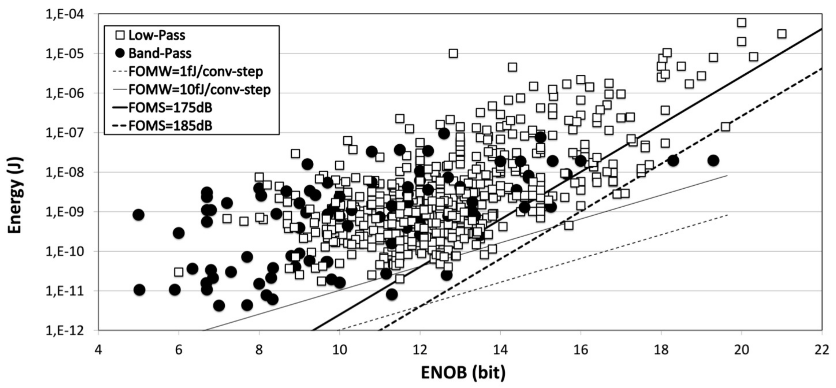
Apart from the main ADC specifications, ENOB and , it is common to compare the efficiency of () ADCs in terms of the amount of energy per converted sample—also referred to as conversion energy, E, defined as [94,95]
where P stands for the power dissipated in Watts (W), and , is the effective Nyquist rate, measured in samples per second (S/s). Figure 13 plots the conversion energy versus ENOB—also known as an energy plot [94,96]. This picture represents graphically the trade-off between resolution and conversion energy such that the larger the resolution, the more conversion energy is needed. It is therefore convenient to express this trade-off in a figure of merit (FOM), which takes into account the main performance metrics of an ADC, i.e., ENOB, and P. The following two FOMs are the most used by the ADC designers community:
where SNDR is related to ENOB as . FOMW, measured in J/conversion-step, was proposed by Walden [97], whereas FOMS is based on a FOM originally proposed by Rabii and Wooley [98], computed on a logarithmic scale, as suggested by Schreier and Temes in [99]. Note that FOMS can be also expressed in the following form:
where denotes the input signal power computed in dB referred to the FS range of the converter. Therefore, the smaller the FOMW value and the larger the FOMS value, the “better” the ADC is. As a reference, FOMW and FOMS are also depicted in Figure 13, considering the following numerical values: FOMW =1 and 10 fJ/conv-step; FOMS = 175 dB and 185 dB. The resulted lines of constant FOMW and FOMS in Figure 13 can be respectively determined from Equation (21) as
As shown, the most efficient designs are based on LP-Ms—mostly implemented with CT circuits—some of them featuring a FOMS between 175 dB and 185 dB [100,101,102,103,104,105,106,107,108].
It is clear from Figure 13 that LP-Ms obtain better performance in terms of conversion energy than BP-Ms. However, it should be noted that the way in which such a conversion energy is computed—based on —might not be adequate for quantifying the efficiency of BP-Ms because is not always representative of the operating frequency of the modulator in this case. For that reason, some authors propose alternative FOMs, such as the following one [109]:
which takes into account not only but also the notch frequency, to measure the conversion energy (E). The reader can note that the use of would increase the number of BP-Ms placed at the cutting edge of the state of the art, although the comparison might be not so fair in this case for LP-Ms. This is illustrated in Figure 14, which shows the conversion energy redefined as
As will be discussed later, new generations of BP-Ms are being developed in order to make RF digitizers more feasible. Thus, it is interesting to compare the performance of BP-Ms in terms of different architectures, circuits and systems techniques. According to the discussion above, especial emphasis will be put not only on but also on .
4.2. Comparison of Different Architectures and Circuits of BP-Ms
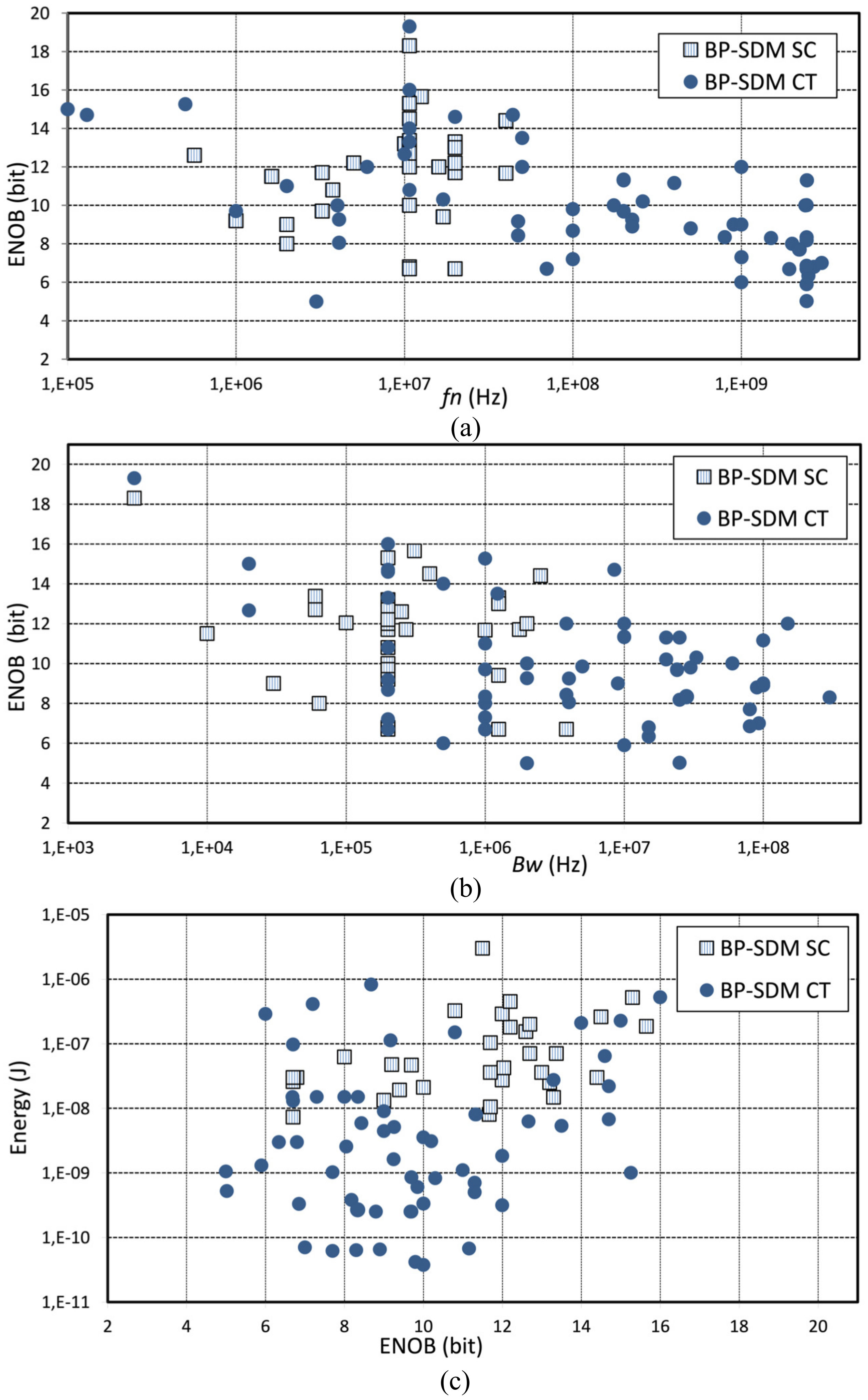
Figure 15a compares the performance of SC and CT BP-Ms by plotting ENOB vs. . As one may expect, the notch frequencies of CT BP-Ms are higher than their SC counterparts. The of SC implementations ranges from 1 MHz to less than 50 MHz, whereas CT BP-Ms digitize signals placed at carrier frequencies ranging from 100 kHz to 3 GHz [34]. The same happens if the digitized bandwidth, , is considered as depicted in Figure 15b. In this case, CT BP-Ms also covers a wider range of , ranging from 3 kHz to almost 300 MHz [88], with 19.3-bit to 8.3-bit ENOB, respectively. More details about the performance metrics achieved by SC and CT BP-Ms are shown in Table 1 and Table 2, respectively. Under similar requirements, the energy consumed by CT BP-Ms is less than that obtained by SC BP-Ms as illustrated in the energy plot shown in Figure 15c.
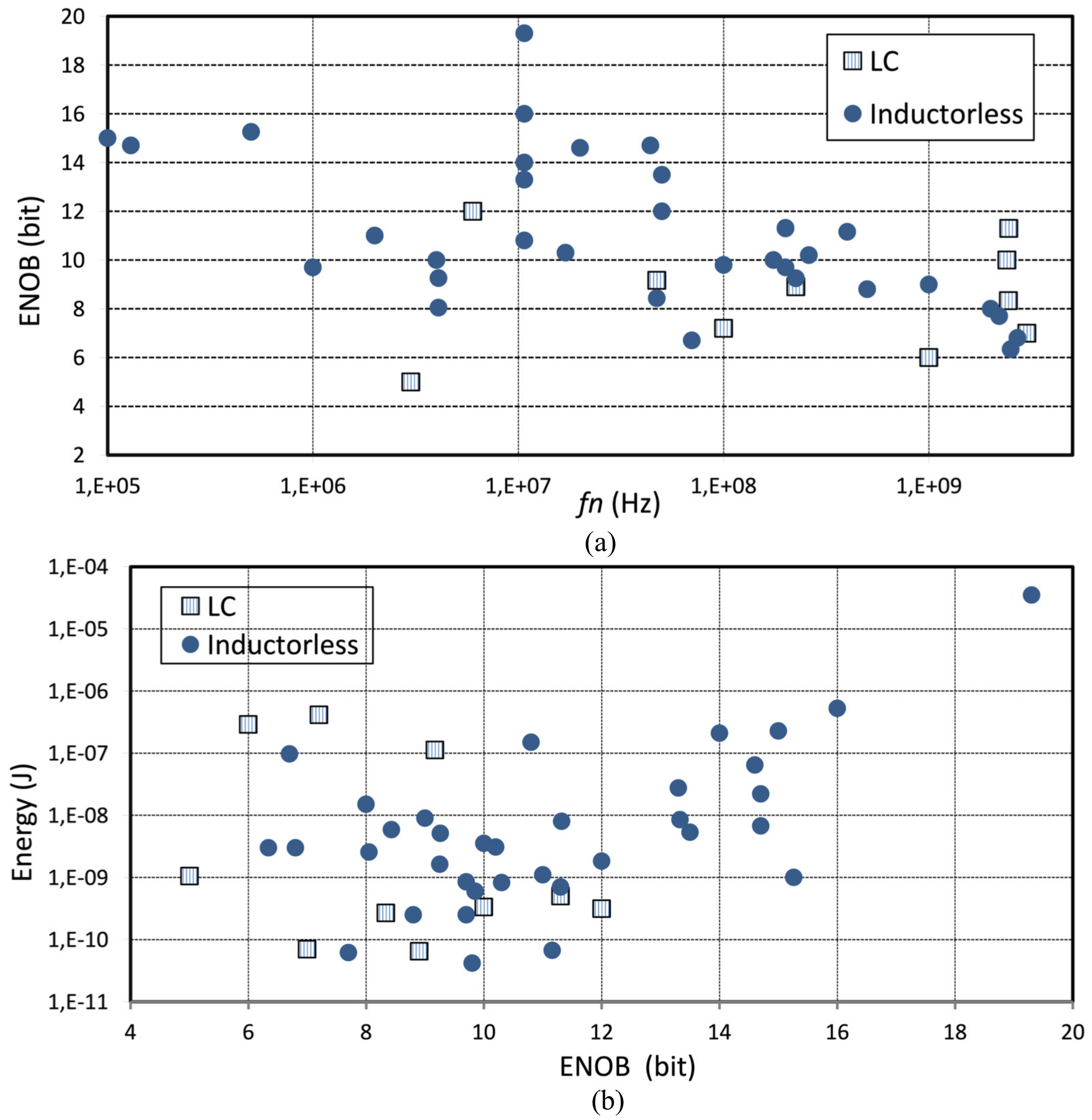
Figure 16 compares CT BP-Ms in terms of the circuit techniques used to implement the loop filter (LF), namely, LC-based or inductorless, i.e., Gm-C, and active-RC. Although the highest notch frequencies are reached by LC-based BP-Ms, there is not a clear advantage with respect to inductorless implementations as depicted in Figure 16a. In terms of energy, inductorless implementations are more efficient as illustrated in Figure 16b, reaching higher resolutions (over 12-bit ENOB). Contrary to what might be expected, LC-based BP-Ms are not necessarily better to digitize RF signals when compared to BP-Ms based on active-RC/Gm-C resonators.
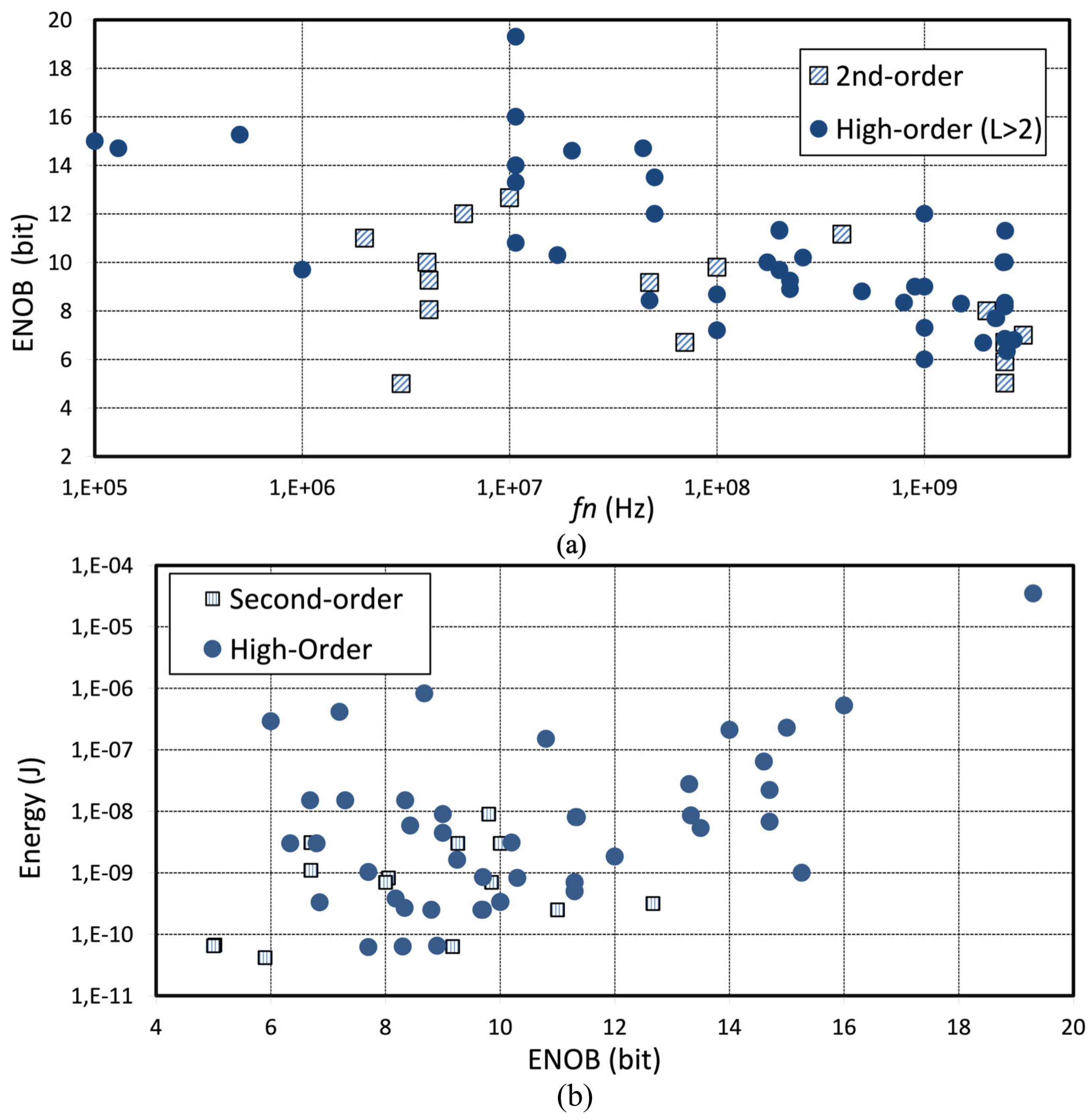
Figure 17 shows the performance of CT BP-Ms in terms of the loop-filter order, L, by comparing those architectures with a 2nd-order () loop filter and those with . There is not a clear benefit in terms of frequency operation by increasing the order, as shown in Figure 17a, although the ENOB improves with L, as expected. However, if the target ENOB is less than 12-bit, 2nd-order loop filters are more energy efficient than high-order architectures as illustrated in Figure 17b.
Figure 18 compares single-bit vs. multi-bit CT BP-Ms. The vast majority of BP-Ms uses a single-bit quantizer and dominates the state of the art, both in terms of frequency range, Figure 18a, and energy efficiency, Figure 18b. Multi-bit implementations are only advantageous if bit, although there are more single-bit BP-Ms featuring higher resolutions in a wider tuning frequency range. This result is somehow logical since multi-bit quantization involves more complex dynamics in the loop filter, especially in the fast loop of CT BP-Ms. This is especially limiting when GHz-range clock signals are required.
4.3. Lessons Learned from State-of-the-Art BP-Ms
From the analysis of the state of the art described above, it can be concluded that low-order (), single-bit CT BP-Ms are the best architectures in terms of operating frequency (), ENOB and conversion energy. However, regardless of the architecture and circuit technique used, BP-Ms are not competitive yet with their LP counterparts, which explains why direct-conversion receivers are the preferred choice in mobile terminals even though they are sensitive to analog impairments of I/Q downconversion. In order to make BP-Ms more efficient for RF ADCs in SDR, it is needed to adopt circuit techniques which can increase the carrier (notch) frequency programmability, with reduced power consumption and (analog) hardware complexity.
Where the loop filter (LF) is concerned, highly programmable scaling-friendly amplifier stages, such as those based on inverter-based OTAs—originally proposed by Nauta [110]—are good candidates to implement both LC-based and active-(GmC) resonators. These circuits have been mostly used in LP-Ms, but very little has been done in BP-Ms [54]. Hybrid active/passive circuits, such as those used by Chae et al. [49], can be exploited to reduce the power dissipation of GHz-range BP-Ms. Moreover, switchable passive RC networks are also suited to implement reconfigurable LFs as well as frequency interleaving [88] and N-path structures. The latter has been used in BP-Ms, although limited to carrier frequencies in the range of hundreds of MHz [87]. However, N-path filters have demonstrated a widely tuning range in GHz filters [111]. This feature should be exploited in BP-M RF ADCs.
Regarding the quantizer, a 1-bit ADC, i.e., a simple (regenerative latch) comparator, is the preferred choice by most state-of-the-art BP-Ms. Multi-bit quantization increases hardware complexity and dynamic requirements in GHz-clocked BP-Ms, as well as the linearity specifications of the feedback DAC. However, single-bit CT BP-Ms are more sensitive to clock jitter, which becomes one of the main limiting factors in RF ADCs. This problem can be palliated by using a finite-impulse response (FIR) feedback DAC since it filters the FS comparator output such that a two-level data sequence is transformed into multi-level data. This reduces the height of steps in the DAC waveform, thus reducing the magnitude of the error signal exciting the LF of the BP-M. FIR-DACs have been widely used in CT LP-Ms, but their benefits have not been exploited yet in BP-Ms.
5. Conclusions
An early digitization is desired in multi-mode/multi-standard wireless transceivers and SDR systems. This approach allows to move most of the signal processing from the analog to the digital domain, thus benefiting from technology downscaling and a higher programmability. BP-Ms are a priori the best candidates to implement RF ADCs in SDRs since they directly digitize RF signals without the need for downmixing them to the baseband. In spite of these benefits, BP-Ms are less efficient than LP-Ms due to the demanding specifications required for the loop-filter circuit to operate at GHz carrier or notch frequencies. The lessons learned from the analysis of the state of the art on BP-Ms carried out in this paper yield the following conclusions:
- System-level: A more simple BP-M architecture—based on a 2nd- or 4th-order loop filter and a 1-bit quantizer—achieves cutting-edge performance, being a good choice that balances performance and efficiency.
- Circuit-level: There are some circuit strategies which can improve the performance of BP-Ms in terms of power consumption, scaling and reconfigurability. Among others, the following techniques are good candidates: inverter-based OTAs, N-path filtering, FIR-filtered feedback DAC and embedded time/frequency-interleaving topologies.
The combination of the above circuits and systems strategies can enhance the efficiency of BP-Ms to digitize RF signals with the specifications required for SDR transceivers: 8-to-12 bit effective resolution within a programmable 30 kHz-to-300 MHz bandwidth and a tunable carrier frequency ranging from 0.4 GHz to 6 GHz.
Thirty years after the first BP-M chip was published, the path toward an efficient RF ADC might be closer to making SDR-based mobile handsets a reality.
Funding
This work was supported in part by Grant PID2019-103876RB-I00, funded by MCIN/AEI/10.13039/501100011033, by the European Union “ESF Investing in your future”, and by “Junta de Andalucía” under contract P20-00599.
Institutional Review Board Statement
Not applicable.
Informed Consent Statement
Not applicable.
Data Availability Statement
Not applicable.
Conflicts of Interest
The authors declare no conflict of interest.
References
- Letaief, K.B.; Chen, W.; Shi, Y.; Zhang, J.; Zhang, Y.-J.A. The Roadmap to 6G: AI Empowered Wireless Networks. IEEE Commun. 2019, 57, 84–90. [Google Scholar] [CrossRef] [Green Version]
- Loh, K. Fertilizing AIoT from Roots to Leaves. In Proceedings of the 2020 IEEE International Solid- State Circuits Conference—(ISSCC), San Francisco, CA, USA, 16–20 February 2020. [Google Scholar]
- Liu, M. Unleashing the Future of Innovation. In Proceedings of the 2021 IEEE International Solid- State Circuits Conference (ISSCC), San Francisco, CA, USA, 13–22 February 2021; pp. 9–16. [Google Scholar]
- Park, S.M.; Kim, Y.G. A Metaverse: Taxonomy, Components, Applications, and Open Challenges. IEEE Access 2022, 10, 4209–4251. [Google Scholar] [CrossRef]
- Bagheri, R.; Mirzaei, A.; Heidari, M.E.; Chehrazi, S.; Lee, M.; Mikhemar, M.; Abidi, A.A. Software-Defined Radio Receiver: Dream to Reality. IEEE Commun. Mag. 2006, 44, 111–118. [Google Scholar] [CrossRef]
- Desoli, G.; Filippi, E. An Outlook on the Evolution of Mobile Terminals: From Monolithic to Modular Multiradio, Multiapplication Platforms. IEEE Circuits Syst. Mag. 2006, 6, 17–29. [Google Scholar] [CrossRef]
- Rubestein, R. Radios Get Smart. IEEE Spectr. 2007, 44, 47–50. [Google Scholar]
- Abidi, A.A. The Path to the Software-Defined Radio Receiver. IEEE J.-Solid-State Circuits 2007, 42, 954–966. [Google Scholar] [CrossRef]
- Machado, R.G.; Wyglinski, A.M. Software-Defined Radio: Bridging the Analog/Digital Divide. Proc. IEEE 2015, 103, 409–423. [Google Scholar] [CrossRef]
- Bhagavatula, V. Exploring Multimode Cellular Transceiver Design: A Short Tutorial. IEEE Solid-State Circuits Mag. 2021, 13, 35–47. [Google Scholar] [CrossRef]
- Mitola, J. The Software Radio Architecture. IEEE Commun. Mag. 1995, 33, 26–38. [Google Scholar] [CrossRef]
- Tasic, A.; Serdijn, W.A.; Long, J.R. Adaptive Multi-Standard Circuits and Systems for Wireless Communications. IEEE Circuits Syst. Mag. 2006, 6, 29–37. [Google Scholar] [CrossRef]
- Mak, P.; Seng-Pan, U.; Martins, R. Transceiver Architecture Selection: Review, State-of-the-Art Survey and Case Study. IEEE Circuits Syst. Mag. 2007, 7, 6–25. [Google Scholar] [CrossRef]
- De la Rosa, J.M.; Castro-Lopez, R.; Morgado, A.; Becerra-Alvarez, E.C.; del Rio, R.; Fernández, F.V.; Perez-Verdu, B. Adaptive CMOS Analog Circuits for 4G Mobile Terminals—Review and State-of-the-Art Survey. Microelectron. J. 2009, 40, 156–176. [Google Scholar] [CrossRef]
- Opteynde, F. A maximally-digital radio receiver front-end. In Proceedings of the 2010 IEEE International Solid-State Circuits Conference—(ISSCC), San Francisco, CA, USA, 7–11 February 2010. [Google Scholar]
- Koli, K.; Kallioinen, S.; Jussila, J.; Sivonen, P.; Parssinen, A. A 900-MHz Direct Delta-Sigma Receiver in 65-nm CMOS. IEEE J. Solid-State Circuits 2010, 45, 2807–2818. [Google Scholar] [CrossRef]
- De la Rosa, J.M. AI-Managed Cognitive Radio Digitizers. IEEE Circuits Syst. Mag. 2022, 22, 10–39. [Google Scholar] [CrossRef]
- Schreier, R.; Snelgrove, M. Bandpass Sigma-Delta Modulation. IET Electron. Lett. 1989, 25, 1560–1561. [Google Scholar] [CrossRef] [Green Version]
- Gailus, P.H. Method and Arrangement for a Sigma Delta Converter for Bandpass Signals. U.S. Patent 4,857,828, 28 January 1989. [Google Scholar]
- Ryckaert, J.; Borremans, J.; Verbruggen, B.; Bos, L.; Armiento, C.; Craninckx, J.; van der Plas, G. A 2.4 GHz Low-Power Sixth-Order RF Bandpass ΔΣ Converter in CMOS. IEEE J. Solid-State Circuits 2009, 44, 2873–2880. [Google Scholar] [CrossRef]
- Beilleau, N.; Aboushady, H.; Montaudon, F.; Cathelin, A. A 1.3 V 26 mW 3.2GS/s Undersampled LC Bandpass ΣΔ ADC for a SDR ISM-band Receiver in 130 nm CMOS. In Proceedings of the IEEE Radio Frequency Integrated Circuits (RFIC) Symposium, Boston, MA, USA, 7–9 June 2009. [Google Scholar]
- Ryckaert, J.; Geis, A.; Bos, L.; van der Plas, G.; Craninckx, J. A 6.1 GS/s 52.8 mW 43 dB DR 80MHz Bandwdith 2.4 GHz RF Bandpass ΔΣ ADC in 40 nm CMOS. In Proceedings of the 2010 IEEE Radio Frequency Integrated Circuits Symposium, Anaheim, CA, USA, 23–25 May 2010; pp. 443–446. [Google Scholar]
- Martens, E.; Bourdoux, A.; Couvreur, A.; Fasthuber, R.; Van Wesemael, P.; Van der Plas, G.; Craninckx, J.; Ryckaert, J. RF-to-Baseband Digitization in 40 nm CMOS with RF Bandpass ΔΣ Modulator and Polyphase Decimation Filter. IEEE J. Solid-State Circuits 2012, 47, 990–1002. [Google Scholar] [CrossRef]
- Shibata, H.; Shibata, H.; Schreier, R.; Yang, W.; Shaikh, A.; Paterson, D.; Caldwell, T.; Alldred, D.; Lai, P.W. A DC-to-1 GHz Tunable RF ΔΣ ADC Achieving DR = 7 4dB and BW = 150 MHz at f0= 450 MHz Using 550 mW. In Proceedings of the 2012 IEEE International Solid-State Circuits Conference, San Francisco, CA, USA, 19–23 February 2012. [Google Scholar]
- Gupta, S.; Gangopadhyay, D.; Lakdawala, H.; Rudell, J.C.; Allstot, D.J. A 0.8-2 GHz Fully-Integrated QPLL-Timed Direct-RF-Sampling Bandpass ΣΔ ADC in 0.13 μm CMOS. IEEE J. Solid-State Circuits 2012, 47, 1141–1153. [Google Scholar] [CrossRef]
- Ashry, A.; Aboushady, H. A 4th Order 3.6 GS/s RF ΣΔ ADC with a FoM of 1 pJ/bit. IEEE Trans. Circuits Syst. Regul. Pap. 2013, 60, 2606–2617. [Google Scholar] [CrossRef]
- Englund, M.; Ostman, K.B.; Viitala, O.; Kaltiokallio, M.; Stadius, K.; Koli, K.; Ryynanen, J. A Programmable 0.7-2.7 GHz Direct ΔΣ Receiver in 40 nm CMOS. IEEE J. Solid-State Circ. 2015, 50, 644–655. [Google Scholar] [CrossRef]
- Chae, H.; Flynn, M. A 69 dB SNDR, 25 MHz BW, 800 MS/s Continuous-Time Bandpass ΔΣ Modulator Using a Duty-Cycle-Controlled DAC for Low Power and Reconfigurability. IEEE J. Solid-State Circuits 2016, 51, 649–659. [Google Scholar]
- Patras, C.Z.P.; Haddadi, H. Deep Learning in Mobile and Wireless Networking: A Survey. IEEE Commun. Surv. Tutorials 2019, 21, 2224–2287. [Google Scholar]
- Bell, J.; Flynn, M.P. A Simultaneous Multiband Continuous-Time ΔΣ ADC with 90-MHz Aggregate Bandwidth in 40-nm CMOS. IEEE Solid-State Lett. 2019, 2, 91–94. [Google Scholar] [CrossRef]
- Zhang, Y.; Kinget, P.R.; Pun, K.P. A 0.032-mm2 43.3-fJ/Step 100–200-MHz IF 2-MHz Bandwidth Bandpass ΔΣM Based on Passive N-Path Filters. IEEE J. Solid-State Circuits 2020, 55, 2443–2455. [Google Scholar] [CrossRef]
- Kim, S.; Rhee, J.; Kim, S. A Wide Dynamic Range Multi-Mode Band-Pass Continuous-Time Delta-Sigma Modulator Employing Single-Opamp Resonator with Positive Resistor-Feedback. IEEE Trans. Circuits Syst. Express Briefs 2020, 67, 235–239. [Google Scholar] [CrossRef]
- Kumar, R.A.; Krishnapura, N. Multi-Channel Analog-to-Digital Conversion Techniques Using a Continuous-Time Delta-Sigma Modulator without Reset. IEEE Trans. Circuits Syst. Regul. Pap. 2020, 67, 3693–3703. [Google Scholar] [CrossRef]
- Sayed, A.; Badran, T.; Louërat, M.M.; Aboushady, H. A 1.5-to-3.0 GHz Tunable RF Sigma-Delta ADC with a Fixed Set of Coefficients and a Programmable Loop Delay. IEEE Trans. Circuits Syst. Express Briefs 2020, 67, 1559–1563. [Google Scholar] [CrossRef]
- Ghaedrahmati, H.; Zhou, J.; Staszewski, R.B. A 38.6-fJ/Conv.-Step Inverter-Based Continuous-Time Bandpass ΔΣ ADC in 28 nm Using Asynchronous SAR Quantizer. IEEE Trans. Circuits Syst. Express Briefs 2021, 68, 3113–3117. [Google Scholar] [CrossRef]
- Jie, L.; Chen, H.-W.; Zheng, B.; Flynn, M.P. A 100 MHz-BW 68 dB-SNDR Tuning-Free Hybrid-Loop DSM with an Interleaved Bandpass Noise-Shaping SAR Quantizer. In Proceedings of the 2021 IEEE International Solid- State Circuits Conference (ISSCC), San Francisco, CA, USA, 13–22 February 2021. [Google Scholar]
- De la Rosa, J.M. Sigma-Delta Converters: Practical Design Guide, 2nd ed.; Wiley: Hoboken, NJ, USA, 2018. [Google Scholar]
- Manivannan, S.; Pavan, S. Improved Continuous-Time Delta-Sigma Modulators with Embedded Active Filtering. IEEE Trans. Circuits Syst. Regul. Pap. 2020, 67, 3778–3789. [Google Scholar] [CrossRef]
- De la Rosa, J.M.; Pérez-Verdú, B.; del Río, R.; Medeiro, F.; Rodríguez-Vázquez, A. Bandpass Sigma-Delta A/D Converters: Fundamentals, Architectures and Circuits; Chapter 11 in CMOS Telecom Data Converters; Rodríguez-Vázquez, A., Medeiro, F., Janssens, E., Eds.; Kluwer Academic Publishers: Amsterdam, The Netherlands, 2003. [Google Scholar]
- Louis, L.; Abcarius, J.; Roberts, G.W. An Eigth-Order Bandpass ΔΣ Modulator for A/D Conversion in Digital Radio. IEEE J. Solid-State Circuits 1999, 34, 423–431. [Google Scholar] [CrossRef]
- Molina-Salgado, G.; Morgado, A.; Dolecek, G.J.; de la Rosa, J.M. LC-Based Bandpass Continuous-Time Sigma-Delta Modulators with Widely Tunable Notch Frequency. IEEE Trans. Circuits Syst. Regul. Pap. 2014, 61, 1442–1455. [Google Scholar] [CrossRef] [Green Version]
- Jantzi, S.A.; Martin, K.W.; Sedra, A.S. Quadrature Bandpass ΔΣ Modulation for Digital Radio. IEEE J. Solid-State Circuits 1997, 32, 1935–1950. [Google Scholar] [CrossRef]
- Paulus, T.; Somayajula, S.S.; Miller, T.A.; Trotter, B.; Kyong, C.; Kerth, D.A. A CMOS IF Transceiver with Reduced Analog Complexity. IEEE J. Solid-State Circuits 1998, 33, 2154–2159. [Google Scholar] [CrossRef]
- Cusinato, P.; Tonietto, D.; Stefani, F. A 3.3-V CMOS 10.7-MHz Sixth-Order Bandpass ΣΔ Modulator with 74-dB Dynamic Range. IEEE J. Solid-State Circuits 2001, 36, 629–638. [Google Scholar] [CrossRef]
- Ong, A.K.; Wooley, B.A. A Two-Path Bandpass ΣΔ Modulator for Digital IF Extraction at 20 MHz. IEEE J. Solid-State Circuits 1997, 32, 1920–1934. [Google Scholar] [CrossRef]
- Ferragina, V.; Fornasari, A.; Gatti, U.; Malcovati, P.; Maloberti, F. Gain and Offset Mismatch Calibration in Time-Interleaved Multipath A/D Sigma-Delta Modulators. IEEE Trans. Circuits Syst. Regul. Pap. 2004, 51, 2365–2373. [Google Scholar] [CrossRef]
- Feng, D.; Maloberti, F.; Sin, S.W.; Martins, R.P. Polyphase Decomposition for Tunable Band-Pass Sigma-Delta A/D Converters. IEEE J. Emerg. Sel. Top. Circuits Syst. 2015, 5, 537–547. [Google Scholar] [CrossRef]
- De la Rosa, J.M.; Schreier, R.; Pun, K.P.; Pavan, S. Next-Generation Delta-Sigma Converters: Trends and Perspectives. IEEE J. Emerg. Sel. Top. Circuits Syst. 2015, 5, 484–499. [Google Scholar] [CrossRef]
- Chae, H.; Jeong, J.; Manganaro, G.; Flynn, M.P. A 12 mW Low Power Continuous-Time Bandpass ΔΣ Modulator with 58 dB SNDR and 24 MHz Bandwidth at 200 MHz IF. IEEE J. Solid-State Circuits 2013, 49, 405–415. [Google Scholar] [CrossRef]
- Shoaei, O.; Snelgrove, W.M. Design and Implementation of a Tunable 40 MHz-70MHz Gm-C Bandpass ΔΣ Modulator. IEEE Trans. Circuits Syst. II: Analog. Digit. Signal Process. 1997, 44, 521–530. [Google Scholar] [CrossRef]
- Beilleau, N.; Aboushady, H.; Loureat, M. Using Finite Impulse Response Feedback DACs to design ΣΔ Modulators based on LC Filters. In Proceedings of the 52nd IEEE International Midwest Symposium on Circuits and Systems (MWSCAS 2009), Cancun, Mexico, 2–5 August 2005; pp. 696–699. [Google Scholar]
- Schreier, R. The Delta-Sigma Toolbox. 2011. Available online: http://www.mathworks.com/matlabcentral/fileexchange/19 (accessed on 11 December 2022).
- Pavan, S.; Schreier, R.; Temes, G.C. Understanding Delta-Sigma Data Converters, 2nd ed.; Wiley: Hoboken, NJ, USA, 2017. [Google Scholar]
- Morgado, A.; del Río, R.; de la Rosa, J.M. Design of a power-efficient widely-programmable Gm-LC band-pass sigma-delta modulator for SDR. In Proceedings of the 2016 IEEE International Symposium on Circuits and Systems (ISCAS), Montréal, QC, Canada, 22–25 May 2016. [Google Scholar]
- Jantzi, S.A.; Snelgrove, W.M.; Ferguson, P.F. A Fourth-Order Bandpass Sigma-Delta Modulator. IEEE J. Solid-State Circuits 1993, 28, 282–291. [Google Scholar] [CrossRef]
- Cheung, V.S.; Luong, H.; Ki, W. A 1 V 10.7 MHz Switched-Opamp Bandpass ΣΔ Modulator Using Double-Sampling Finite-Gain-Compensation Technique. IEEE J. Solid-State Circuits 2002, 37, 1215–1225. [Google Scholar] [CrossRef]
- Salo, T.O.; Lindfors, S.; Halonen, K. A 80-MHz Band-pass ΣΔ Modulator for a 100-MHz IF Receiver. IEEE J. Solid-State Circuits 2002, 37, 798–808. [Google Scholar] [CrossRef]
- Cheng, W.T.; Pun, K.P.; Choy, C.S.; Chan, C.F. A 75 dB Image Rejection IF-Input Quadrature Sampling SC ΣΔ Modulator. In Proceedings of the 31st European Solid-State Circuits Conference, Grenoble, France, 12–16 September 2005; pp. 455–458. [Google Scholar]
- Song, B.S. A Fourth-Order Bandpass Delta-Sigma Modulator with Reduced Number of Op Amps. IEEE J. Solid-State Circuits 1995, 30, 1309–1315. [Google Scholar] [CrossRef]
- Kuo, C.H.; Liu, S.I. A 1-V 10.7-MHz Fourth-Order Bandpass ΔΣ Modulators Using Two Switched Opamps. IEEE J. Solid-State Circuits 2004, 39, 2041–2045. [Google Scholar]
- Ueno, T.; Yasuda, A.; Yamaji, T.; Itakura, T. A Fourth-Order Bandpass Δ − Σ Modulator Using Second-Order Bandpass Noise-Shaping Dynamic Element Matching. IEEE J. Solid-State Circuits 2001, 37, 522–525. [Google Scholar] [CrossRef]
- Hairapetian, A. An 81 MHz IF receiver in CMOS. IEEE J. Solid-State Circuits 1996, 31, 1981–1986. [Google Scholar] [CrossRef]
- Tabatabaei, A.; Wooley, A. A Two-Path Bandpass Sigma-Delta Modulator with Extended Noise Shaping. IEEE J. Solid-State Circuits 2000, 35, 1799–1809. [Google Scholar] [CrossRef]
- Salo, T.O.; Lindfors, S.J.; Hollman, T.M.; Jarvinen, J.A.M.; Halonen, K.A. 80-MHz Bandpass ΔΣ Modulators for Multimode Digital IF Receivers. IEEE J. Solid-State Circuits 2003, 38, 464–474. [Google Scholar] [CrossRef]
- Galdi, I.; Bonizzoni, E.; Maloberti, F.; Manganaro, G.; Malcovati, P. Two-Path Band-Pass ΣΔ Modulator with 40-MHz IF 72-dB DR at 1-MHz Bandwidth Conuming 16mW. In Proceedings of the 2007 IEEE International Solid- State Circuits Conference, San Francisco, CA, USA, 11–15 February 2007; pp. 248–251. [Google Scholar]
- Yamamoto, T.; Kasahara, M.; Matsuura, T. A 63 mA 112/94 dB DR IF Bandpass ΔΣ Modulator with Direct Feed-Forward Compensation and Double Sampling. IEEE J. Solid-State Circuits 2008, 43, 1783–1794. [Google Scholar] [CrossRef]
- Maurino, R.; Papavassiliou, C. A 10 mW 81 dB Cascaded Multibit Quadrature ΣΔ ADC with a Dynamic Element Matching Scheme. In Proceedings of the 31st European Solid-State Circuits Conference, Grenoble, France, 12–16 September 2005; pp. 451–454. [Google Scholar]
- Yamamoto, K.; Carusone, A.C.; Dawson, F.P. A Delta-Sigma Modulator with a Widely Programmable Center Frequency and 82-dB Peak SNDR. In Proceedings of the 2007 IEEE Custom Integrated Circuits Conference. (CICC 07), San Jose, CA, USA, 16–19 September 2007; pp. 65–69. [Google Scholar]
- Ying, F.; Maloberti, F. A mirror image free two-path bandpass ΣΔ modulator with 72 dB SNR and 86 dB SFDR. IEEE ISSCC Dig. Tech. Pap. 2004, 84–85. [Google Scholar]
- Thomas, K.P.J.; Rana, R.S.; Lian, Y. A 1 GHz CMOS Fourth-Order Continuous-Time Bandpass Sigma-Delta Modulator for RF Receiver Front-End A/D Conversion. In Proceedings of the ASPDAC05: Asia and South Pacific Design Automation Conference, Shanghai, China, 18–21 January 2005; pp. 665–670. [Google Scholar]
- Tao, H.; Khoury, J.M. A 400-MS/s Frequency Translating Bandpass Sigma-Delta Modulator. IEEE J. Solid-State Circuits 1999, 34, 1741–1752. [Google Scholar] [CrossRef]
- Hsu, I.; Luong, H.C. A 70-MHz Continuous-Time CMOS Band-pass ΣΔ Modulator for GPS Receivers. In Proceedings of the IEEE International Symposium on Circuits and Systems, ISCAS 2000, Geneva, Switzerland, 28–31 May 2000; pp. 750–753. [Google Scholar]
- Chopp, P.M.; Hamoui, A. A 1-V 13-mW Single-Path Frequency-Translating ΔΣ Modulator with 55-dB SNDR and 4-MHz Bandwidth at 225 MHz. IEEE J. Solid-State Circuits 2013, 48, 473–486. [Google Scholar] [CrossRef]
- Yu, R.; Xu, Y.P. Bandpass Sigma-Delta Modulator Employing SAW Resonator as Loop Filter. IEEE Trans. Circuits Syst. Regul. Pap. 2007, 54, 723–735. [Google Scholar] [CrossRef]
- Gupta, S.; Gangopadhyay, D.; Lakdawala, H.; Rudell, J.C.; Allstot, D.J. A QPLL-Timed Direct-RF Sampling Band-Pass ΣΔ ADC with a 1.2 GHz Tuning Range in 0.13 μm CMOS. In Proceedings of the 2011 IEEE Radio Frequency Integrated Circuits Symposium, Baltimore, MD, USA, 5–7 June 2011. [Google Scholar]
- Engelen, J.V.; van de Plassche, R. BandPass Sigma-Delta Modulators: Stability Analysis, Performance and Design Aspects; Kluwer Academic Publishers: Amsterdam, The Netherlands, 1999. [Google Scholar]
- Englund, M.; Ostman, K.B.; Viitala, O.; Kaltiokallio, M.; Stadius, K.; Ryynanen, J.; Koli, K. A 2.5-GHz 4.2-dB NF Direct ΔΣ Receiver with a Frequency-Translating Integrator. In Proceedings of the 40th European Solid State Circuits Conference (ESSCIRC 2014), Venice, Italy, 22–26 September 2014; pp. 371–374. [Google Scholar]
- Kim, S.B.; Joeres, S.; Zimmermann, N.; Robens, M.; Wunderlich, R.; Heinen, S. Continuous-Time Quadrature Bandpass Sigma-Delta Modulator for GPS/Galileo Low-IF Receiver. In Proceedings of the 2007 IEEE Radio Frequency Integrated Circuits (RFIC), Honolulu, HI, USA, 3–5 June 2007; pp. 127–130. [Google Scholar]
- Chopp, P.M.; Hamoui, A.A. A 1V 13 mW Frequency-Translating ΔΣ ADC with 55dB SNDR for a 4MHz Band at 225MHz. In Proceedings of the 2011 IEEE Custom Integrated Circuits Conference (CICC 2011), San Jose, CA, USA, 19–21 September 2021. [Google Scholar]
- Ashry, A.; Aboushady, H. A 3.6 GS/s, 15 mW, 50 dB SNDR, 28 MHz Bandwidth RF ΣΔ ADC with FoM of 1 pJ/bit in 130 nm CMOS. In Proceedings of the 2011 IEEE Custom Integrated Circuits Conference (CICC 2011), San Jose, CA, USA, 19–21 September 2021. [Google Scholar]
- Veldhoven, R.H.M. A Triple-Mode Continuous-Time ΣΔ Modulator with Switched-Capacitor Feedback DAC for a GSM-EDGE/CDMA2000/UMTS Receiver. IEEE J. Solid-State Circuits 2003, 38, 2069–2076. [Google Scholar] [CrossRef]
- Van der Zwan, E.J.; Philips, K.; Bastiaansen, C.A.A. A 10.7-MHz IF-to-Baseband ΣΔ A/D Conversion System for AM/FM Radio Receivers. IEEE J. Solid-State Circuits 2000, 35, 1810–1819. [Google Scholar] [CrossRef] [Green Version]
- Kappes, M.S. A 2.2-mW CMOS Bandpass Continuous-Time Multibit Δ − Σ ADC with 68 dB of Dynamic Range and 1-MHz Bandwidth for Wireless Applications. IEEE J. Solid-State Circuits 2003, 38, 1098–1104. [Google Scholar] [CrossRef]
- Silva, P.G.; Breems, L.J.; Makinwa, K.A.; Roovers, R.; Huijsing, J.H. An IF-to-Baseband ΣΔ Modulator for AM/FM/IBOC Radio Receivers with a 118 dB Dynamic Range. IEEE J. Solid-State Circuits 2007, 42, 1076–1089. [Google Scholar] [CrossRef]
- Jeong, J.; Collins, N.; Flynn, M. A 260 MHz IF Sampling Bit-Stream Processing Digital Beamformer with an Integrated Array of Continuous-Time Band-Pass ΔΣ Modulators. IEEE J. Solid-State Circuits 2016, 51, 1168–1176. [Google Scholar] [CrossRef]
- Lu, C.Y.; Silva-Rivas, J.F.; Kode, P.; Silva-Martinez, J.; Hoyos, S. A Sixth-Order 200 MHz IF Bandpass Sigma-Delta Modulator with Over 68 dB SNDR in 10 MHz Bandwidth. IEEE J. Solid-State Circuits 2010, 45, 1122–1136. [Google Scholar] [CrossRef]
- Zhang, C.; Ueng, Y.L.; Studer, C.; Burg, A. Artificial Intelligence for 5G and Beyond 5G: Implementations, Algorithms, and Optimizations. IEEE J. Emerg. Sel. Top. Circuits Syst. 2020, 10, 149–163. [Google Scholar] [CrossRef]
- Lu, R.; Flynn, M.P. A 300 MHz-BW 38 mW 37 dB/40 dB SNDR/DR Frequency-Interleaving Continuous-Time Bandpass Delta-Sigma ADC in 28 nm CMOS. In Proceedings of the 2021 Symposium on VLSI Circuits, Kyoto, Japan, 13–19 June 2021. [Google Scholar]
- Kim, S.B.; Joeres, S.; Wunderlich, R.; Heinen, S. A 2.7 mW, 90.3 dB DR Continuous-Time Quadrature Bandpass Sigma-Delta Modulator for GSM/EDGE Low-IF Receiver in 0.25 μm CMOS. IEEE J. Solid-State Circuits 2009, 44, 891–900. [Google Scholar] [CrossRef]
- Chae, Y.; Souri, K.; Makinwa, K.A. A 6.3 μW 20 bit Incremental Zoom-ADC with 6 ppm INL and 1 μV Offset. IEEE J. Solid-State Circuits 2013, 48, 3019–3027. [Google Scholar] [CrossRef] [Green Version]
- Harrison, J.; Nesselroth, M.; Mamuad, R.; Behzad, A.; Adams, A.; Avery, S. An LC Bandpass ΔΣ ADC with 70 dB SNDR Over 20 MHz Bandwidth Using CMOS DACs. In Proceedings of the 2012 IEEE International Solid-State Circuits Conference, San Francisco, CA, USA, 19–23 February 2012. [Google Scholar]
- Xu, Y.; Zhang, Z.; Chi, B.; Liu, Q.; Zhang, X.; Wang, Z. Dual-mode 10 MHz BW 4.8/6.3 mW Reconfigurable Lowpass/ Complex Bandpass CT ΣΔ Modulator with 65.8/74.2dB DR for a Zero/Low-IF SDR Receiver. In Proceedings of the 2014 IEEE Radio Frequency. Integrated Circuits Symposium, Tampla, FL, USA, 1–3 June 2014; pp. 313–316. [Google Scholar]
- Schreier, R.; Abaskharoun, N.; Shibata, H.; Paterson, D.; Rose, S.; Mehr, I.; Luu, Q. A 375-mW Quadrature Bandpass ΔΣ ADC with 8.5-MHz BW and 90-dB DR at 44 MHz. IEEE J. Solid-State Circuits 2006, 41, 2632–2640. [Google Scholar] [CrossRef]
- Murmann, B. A/D Converter Trends: Power Dissipation, Scaling and Digitally Assisted Architectures. In Proceedings of the 2008 IEEE Custom Integrated Circuits Conference, San Jose, CA, USA, 21–24 September 2008; pp. 105–112. [Google Scholar]
- Jonsson, B.E. An Empirical Approach to Finding Energy Efficient ADC Architectures. In Proceedings of the 2011 International Workshop on ADC Modelling, Testing and Data Converter Analysis and Design and IEEE 2011 ADC Forum, Orvieto, Italy, 30 June–1 July 2011. [Google Scholar]
- Manganaro, G. Advanced Data Converters; Cambridge University Press: Cambridge, UK, 2012. [Google Scholar]
- Walden, R.H. Analog-to-Digital Converter Survey and Analysis. IEEE J. Sel. Areas Commun. 1999, 17, 539–550. [Google Scholar] [CrossRef] [Green Version]
- Rabii, S.; Wooley, B.A. A 1.8 V Digital-Audio Sigma-Delta Modulator in 0.8 μm CMOS. IEEE J. Solid-State Circuits 1997, 32, 783–796. [Google Scholar] [CrossRef] [Green Version]
- Schreier, R.; Temes, G.C. Understanding Delta-Sigma Data Converters.; IEEE Press: New York, NY, USA, 2005. [Google Scholar]
- Pavan, S.; Sankar, P. Power Reduction in Continuous-Time Delta-Sigma Modulators Using the Assisted Opamp Technique. IEEE J. Solid-State Circuits 2010, 45, 1365–1379. [Google Scholar] [CrossRef]
- Shettigar, P.; Pavan, S. Design Techniques for Wideband Single-Bit Continuous-Time ΔΣ Modulators with FIR Feedback DACs. IEEE J. Solid-State Circuits 2012, 47, 2865–2879. [Google Scholar] [CrossRef]
- Shu, Y.S.; Tsai, J.Y.; Chen, P.; Lo, T.Y.; Chiu, P.C. A 28fJ/conv-step CT ΔΣ Modulator with 78 dB DR and 18 MHz BW in 28 nm CMOS Using a Highly Digital Multibit Quantizer. In Proceedings of the 2013 IEEE International Solid-State Circuits Conference Digest of Technical Papers, San Francisco, CA, USA, 17–21 February 2013. [Google Scholar]
- Zeller, S.; Muenker, C.; Weigel, R.; Ussmueller, T. A 0.039 mm2 Inverter-Based 1.82 mW 68.6 dB-SNDR 10 MHz-BW CT-ΣΔ-ADC in 65 nm CMOS Using Power- and Area-Efficient Design Techniques. IEEE J. Solid-State Circuits 2014, 49, 1548–1560. [Google Scholar] [CrossRef]
- Sukumaran, A.; Pavan, S. Low Power Design Techniques for Single-Bit Audio Continuous-Time Delta Sigma ADCs Using FIR Feedback. IEEE J. Solid-State Circuits 2014, 49, 2515–2525. [Google Scholar] [CrossRef]
- Dong, Y.; Yang, W.; Schreier, R.; Sheikholeslami, A.; Korrapati, S. A Continuous-Time 0–3 MASH ADC Achieving 88 dB DR with 53 MHz BW in 28 nm CMOS. IEEE J. Solid-State Circuits 2014, 49, 2868–2877. [Google Scholar] [CrossRef]
- De Berti, C.; Malcovati, P.; Crespi, L.; Baschirotto, A. A 106 dB A-Weighted DR Low-Power Continuous-Time ΣΔ Modulator for MEMS Microphones. IEEE J. Solid-State Circuits 2016, 51, 1607–1618. [Google Scholar] [CrossRef]
- Briseno-Vidrios, C.; Edward, A.; Rashidi, N.; Silva-Martinez, J. A 4 Bit Continuous-Time ΣΔ Modulator with Fully Digital Quantization Noise Reduction Algorithm Employing a 7 Bit Quantizer. IEEE J. Solid-State Circuits 2016, 51, 1398–1409. [Google Scholar] [CrossRef]
- S Mondal, O.G.; Hall, D.A. A 139 μW 104.8dB-DR 24 kHz-BW CTΔΣM with Chopped AC-Coupled OTA-Stacking and FIR DACs. In Proceedings of the 2021 IEEE International Solid- State Circuits Conference (ISSCC), San Francisco, CA, USA, 13–22 February 2021. [Google Scholar]
- Rodríguez-Vázquez, A.; Medeiro, F.; Janssens, E. CMOS Telecom Data Converters; Kluwer Academic Publishers: Amsterdam, The Netherlands, 2003. [Google Scholar]
- Nauta, B. A CMOS Transconductance-C Filter Technique for Very High Frequencies. IEEE J. Solid-State Circuits 1992, 27, 142–153. [Google Scholar] [CrossRef] [Green Version]
- Purushothaman, V.K.; Klumperink, E.A.; Clavera, B.T.; Nauta, B. A Fully Passive RF Front End with 13-dB Gain Exploiting Implicit Capacitive Stacking in a Bottom-Plate N-Path Filter/Mixer. IEEE J. Solid-State Circuits 2020, 55, 1139–1150. [Google Scholar] [CrossRef] [Green Version]
Figure 1.
Software-defined radio transceiver. (a) Ideal concept. (b) Including RF/ASP interface.

Figure 2.
Conceptual diagram of reconfigurable RF transceivers based on the following: (a) Downconversion to baseband. (b) RF-Digitization (quadrature mixers, not drawn for simplicity, are assumed).
Figure 2.
Conceptual diagram of reconfigurable RF transceivers based on the following: (a) Downconversion to baseband. (b) RF-Digitization (quadrature mixers, not drawn for simplicity, are assumed).

Figure 3.
Conceptual block diagram of a M.

Figure 4.
Illustrating the signal processing in a RF Rx based on BP-Ms with .

Figure 5.
Noise-shaping programmability in BP-Ms from to ( GHz).

Figure 6.
LP-to-BP transformation: (a) 2nd-order LP-M, (b) 4th-order BP-M.

Figure 7.
Quadrature BP-Ms. (a) Block diagram of a complex BP filter. (b) NTF with asymmetric placement of zeroes.
Figure 7.
Quadrature BP-Ms. (a) Block diagram of a complex BP filter. (b) NTF with asymmetric placement of zeroes.

Figure 8.
Conceptual block diagram of a TI BP-M.

Figure 9.
(a) Conceptual diagram of BP CT-Ms based on (b) LC-tank resonators, (c) active Gm-C integrators, and (d) single op amp resonators with Q-factor boosting [49].
Figure 9.
(a) Conceptual diagram of BP CT-Ms based on (b) LC-tank resonators, (c) active Gm-C integrators, and (d) single op amp resonators with Q-factor boosting [49].

Figure 10.
Conventional LC BP-Ms with a multi-path feedback loop based on the following: (a) Different DAC (RZ/HRZ) waveforms [50]. (b) Identical DAC (NRZ) with different delay [51].

Figure 11.
Tunable CT BP-Ms. (a) Block diagram, (b) Gm-LC resonator. (c) Output spectra [54].
Figure 11.
Tunable CT BP-Ms. (a) Block diagram, (b) Gm-LC resonator. (c) Output spectra [54].

Figure 12.
Aperture plot of Ms: BP-Ms vs. LP-Ms.

Figure 13.
Energy plot of Ms: BP-Ms vs. LP-Ms.

Figure 14.
Energy plot of Ms using Equation (25) to compute the conversion energy of BP-Ms.
Figure 14.
Energy plot of Ms using Equation (25) to compute the conversion energy of BP-Ms.

Figure 15.
SC vs. CT BP-Ms: (a) ENOB vs. , (b) ENOB vs. . (c) Energy plot.

Figure 16.
LC-based vs. inductorless BP-Ms: (a) ENOB vs. , (b) energy plot.

Figure 17.
Second-order vs. High-order () BP-Ms: (a) ENOB vs. , (b) energy plot.

Figure 18.
Single-bit vs. multi-bit BP-Ms: (a) ENOB vs. , (b) energy plot.


Table 1.
Summary of the state of the art on SC BP-M ICs (sorted by FOMS).
| Ref. | DR (bit) | (MHz) | (MHz) | L | Tech./Sup.Volt | P (mW) | FOMS (dB) |
|---|---|---|---|---|---|---|---|
| [56] | 6.8 | 10.7 | 0.2 | 2 | 0.35 mu/1 V | 12.0 | 115 |
| [57] | 6.7 | 20.0 | 3.84 | 4 | 0.35 mu /3 V | 56.0 | 120 |
| [42] | 10.8 | 3.75 | 0.2 | 4 | 0.8 mu/5 V | 130.0 | 129 |
| [58] | 9.7 | 3.25 | 0.2 | 3 | 0.35 mu/3.3 V | 18.7 | 130 |
| [59] | 9.0 | 2.0 | 0.03 | 4 | 2 mu/3.3 V | 0.8 | 132 |
| [60] | 10.0 | 10.7 | 0.2 | 4 | 0.25 mu/1 V | 8.5 | 136 |
| [44] | 12.0 | 10.7 | 0.2 | 6 | 0.35 mu/3.3 V | 116.0 | 136 |
| [57] | 11.7 | 20.0 | 0.27 | 4 | 0.35 mu/3 V | 56.0 | 139 |
| [45] | 12.2 | 20.0 | 0.2 | 4 | 0.6 mu/3.3 V | 72.0 | 140 |
| [61] | 12.6 | 0.56 | 0.25 | 2-2 | 0.25 mu/2.5 V | 77.0 | 143 |
| [62] | 11.7 | 3.25 | 0.2 | 4-2 | 0.8 mu/3 V | 14.4 | 144 |
| [60] | 12.0 | 10.7 | 0.1 | 4 | 0.25 mu/1 V | 8.5 | 145 |
| [63] | 12.0 | 16.0 | 2.0 | 6 | 0.25 mu/2.5 V | 110.0 | 147 |
| [60] | 12.7 | 10.7 | 0.06 | 4 | 0.25 mu /1 V | 8.5 | 147 |
| [64] | 11.7 | 20.0 | 1.76 | 4-4 | 0.35 mu/3 V | 37.0 | 149 |
| [65] | 11.7 | 40.0 | 1.0 | 4 | 0.18 mu/1.8 V | 16.0 | 150 |
| [60] | 13.4 | 10.7 | 0.06 | 4 | 0.25 mu/1 V | 8.5 | 151 |
| [66] | 14.5 | 10.7 | 0.4 | 4 | 0.15 V/3.3 V | 208.0 | 152 |
| [66] | 18.3 | 10.7 | 0.003 | 4 | 0.15 V/3.3 V | 208.0 | 154 |
| [66] | 15.3 | 10.7 | 0.2 | 4 | 0.15 V/3.3 V | 208.0 | 154 |
| [67] | 13.2 | 10.0 | 0.2 | 2 | 0.25 mu/2.1 V | 10.0 | 154 |
| [64] | 13.3 | 20.0 | 1.25 | 4-4 | 0.35 mu/3 V | 37.0 | 157 |
| [68] | 15.7 | 12.6 | 0.31 | 4 | 0.18 mu/1.8 V | 115.0 | 160 |
| [69] | 14.4 | 40.0 | 2.5 | 4 | 0.18 mu/1.8 V | 150.0 | 161 |
Table 2.
Summary of the state of the art on CT BP-Ms (sorted by FOMS).
| Ref. | DR (bit) | (MHz) | (MHz) | L | Tech./Sup.Volt | P (mW) | FOMS (dB) |
|---|---|---|---|---|---|---|---|
| [70] | 6.0 | 1000 | 0.5 | 4 | 0.18 mu/1.8 V | 290.0 | 61 |
| [71] | 7.2 | 100 | 0.2 | 4 | 0.35 mu/3.3 V | 165.0 | 67 |
| [72] | 6.7 | 70 | 0.2 | 2 | 0.5 mu/2.5 V | 39.0 | 68 |
| [73] | 8.9 | 225 | 100 | 6 | 65 nm/1 V | 13.0 | 90 |
| [74] | 9.2 | 47.3 | 0.2 | 2 | 0.35 mu/3.3 V | 45.0 | 90 |
| [75] | 8.0 | 2000 | 1.0 | 2 | 0.13 mu/1.2 V | 30.0 | 92 |
| [27] | 6.8 | 2700 | 15.0 | 4 | 40 nm/1.1 V | 90.0 | 103 |
| [76] | 10.8 | 10.7 | 0.2 | 6 | 0.5 mu /5 V | 60.0 | 104 |
| [74] | 8.4 | 47.3 | 3.84 | 4 | 0.35 mu/3.3 V | 45.0 | 109 |
| [77] | 6.3 | 2500 | 15.0 | 3 | 40 nm/1.1 V | 90.0 | 109 |
| [78] | 8.1 | 4.09 | 4.0 | 2 | 0.25 mu /1.8 V | 20.5 | 109 |
| [78] | 9.3 | 4.09 | 2.0 | 2 | 0.25 mu/1.8 V | 20.5 | 114 |
| [79] | 9.3 | 228 | 4.0 | 4 | 65 nm/1 V | 13.0 | 122 |
| [80] | 8.3 | 2440 | 28.0 | 4 | 0.13 mu/1.2 V | 15.0 | 129 |
| [81] | 15.0 | 0.1 | 0.02 | 5 | 0.18 mu/2.9 V | 9.1 | 130 |
| [34] | 7.0 | 3000 | 93.0 | 2 | 65 nm/1.2 V | 13.0 | 130 |
| [82] | 13.3 | 10.7 | 0.2 | 5 | 0.25 mu/2.5 V | 11.0 | 133 |
| [83] | 11.0 | 2.0 | 1.0 | 2 | 0.18 mu/1.8 V | 2.2 | 134 |
| [84] | 14.0 | 10.7 | 0.5 | 5 | 0.18 mu/1.8 V | 210.0 | 135 |
| [85] | 10.2 | 260 | 20.0 | 4 | 65 nm/1.4 V | 124.0 | 135 |
| [23] | 7.7 | 2.2 | 80.0 | 4 | 40 nm/1.1 V | 9.86 | 135 |
| [86] | 11.3 | 200 | 10.0 | 4 | 0.18 mu/1.8 V | 160.0 | 137 |
| [84] | 19.3 | 10.7 | 0.003 | 5 | 0.18 mu/1.8 V | 210.0 | 138 |
| [32] | 14.6 | 20.0 | 0.2 | 3 | 180 nm/1.8 V | 25.8 | 142 |
| [49] | 9.7 | 200 | 24.0 | 4 | 65 nm/1.25 V | 12.0 | 142 |
| [87] | 10.0 | 175 | 2.0 | 4 | 65 nm/1 V | 0.15 | 144 |
| [84] | 16.0 | 10.7 | 0.2 | 5 | 0.18 mu/1.8 V | 210.0 | 145 |
| [81] | 12.0 | 50.0 | 3.84 | 5 | 0.18 mu/ 2.9 V | 14.1 | 146 |
| [88] | 8.3 | 1.5 | 300 | 4 | 28 nm/1 V | 38.0 | 147 |
| [20] | 10.0 | 2.4 | 60.0 | 6 | 90 nm/1 V | 40.0 | 148 |
| [81] | 13.5 | 50.0 | 1.23 | 5 | 0.18 mu/2.9 V | 13.1 | 150 |
| [28] | 11.3 | 180 | 25.0 | 6 | 65 nm/1.2 V | 35.0 | 152 |
| [35] | 9.8 | 100 | 30.0 | 2 | 28 nm/1 V | 2.5 | 152 |
| [89] | 14.7 | 0.13 | 0.2 | 3 | 0.25 mu/1.8 V | 2.7 | 152 |
| [90] | 11.3 | 200 | 25.0 | 6 | 65 nm/1 V | 35.0 | 153 |
| [91] | 11.3 | 2.45 | 20.0 | 6 | 40 nm/1.1 V | 20.0 | 153 |
| [92] | 12.0 | 6.0 | 10.0 | 2 | 65 nm/1.2 V | 6.3 | 158 |
| [93] | 14.7 | 44.0 | 8.5 | 4 | 0.18 mu/2.9 V | 375 | 163 |
| [36] | 11.2 | 400 | 100 | 2 | 28 nm/1 V | 13.4 | 167 |
Disclaimer/Publisher’s Note: The statements, opinions and data contained in all publications are solely those of the individual author(s) and contributor(s) and not of MDPI and/or the editor(s). MDPI and/or the editor(s) disclaim responsibility for any injury to people or property resulting from any ideas, methods, instructions or products referred to in the content. |
© 2023 by the author. Licensee MDPI, Basel, Switzerland. This article is an open access article distributed under the terms and conditions of the Creative Commons Attribution (CC BY) license (https://creativecommons.org/licenses/by/4.0/).
Share and Cite
MDPI and ACS Style
de la Rosa, J.M. Bandpass Sigma–Delta Modulation: The Path toward RF-to-Digital Conversion in Software-Defined Radio. Chips 2023, 2, 44-69. https://doi.org/10.3390/chips2010004
AMA Style
de la Rosa JM. Bandpass Sigma–Delta Modulation: The Path toward RF-to-Digital Conversion in Software-Defined Radio. Chips. 2023; 2(1):44-69. https://doi.org/10.3390/chips2010004
Chicago/Turabian Stylede la Rosa, Jose M. 2023. "Bandpass Sigma–Delta Modulation: The Path toward RF-to-Digital Conversion in Software-Defined Radio" Chips 2, no. 1: 44-69. https://doi.org/10.3390/chips2010004