
Methodology for a Low-Power and Low-Circuit-Area 15-Bit SAR ADC Using Split-Capacitor Mismatch Compensation and a Dynamic Element Matching Algorithm


Departement of Reliable RF and Mixed-Signal, University Grenoble Alpes, CNRS, Grenoble INP*, TIMA, 38000 Grenoble, France
*
Authors to whom correspondence should be addressed.
Chips 2023, 2(1), 31-43; https://doi.org/10.3390/chips2010003
Submission received: 11 November 2022
/
Revised: 10 February 2023
/
Accepted: 14 February 2023
/
Published: 27 February 2023
Abstract
:This paper presents a design methodology for a low-power, low-chip-area, and high-resolution successive approximations register (SAR) analog-to-digital converter (ADC). The proposed method includes a segmented capacitive DAC (C-DAC) to reduce the power consumption and the total area. An embedded self-calibration algorithm based on a set of trimming capacitors was applied alongside a dynamic element matching (DEM) procedure to control the inherent linearity issues caused by the process mismatch. The SAR ADC and each additional algorithm were modeled in MATLAB to show their efficiency. Finally, a simple methodology was developed to allow for the fast estimation of signal-to-noise ratios (SNRs) without any FFT calculation.
1. Introduction
The expansion of the Internet of Things has increased the need for ultra-low-power analog-to-digital converters (ADCs). Autonomous applications such as medical devices, wireless sensors, and space instruments must deal with the major issue of power dissipation. However, reducing ADC power consumption is very challenging. Thanks to their simple structure and capacity to take full advantage of process scaling, successive approximations register (SAR) ADCs present a good figure of merit, which makes them a promising choice for low-power applications. However, since the number of clock periods needed for one conversion is proportional to the resolution, this architecture cannot easily reach a high-speed resolution. To achieve a high resolution with SAR ADCs, each energy-consuming element must be carefully considered, along with sources of mismatch, noise, and any other limitations.
Several types of DAC architecture are available for implementation into a SAR ADC: capacitor-based DAC (C-DAC) [1,2,3,4,5,6], switched current DAC [7,8,9], and R-2R ladder DAC [10,11]. To reduce the DC power dissipation, the majority of SAR ADCs are based on charge redistribution algorithms using a sampled array of capacitors. Monotonic architecture [12,13] shows superior power dissipation and linearity compared to the classical algorithm; however, the former shows a non-constant common mode. Vmc-based switching architectures [14,15] also present better power features while keeping a constant common mode.
For high-resolution designs, the power consumption and the total chip area of the capacitor array become an issue in addition to the mismatch. In this work, segmentation in the capacitors array was used as one solution to the chip area issue [6,16]. Nevertheless, a segmented architecture increases sensitivity to the capacitors’ mismatch; thus, an additional digital calibration algorithm is necessary [16,17,18,19,20,21,22]. Many digital calibration architectures are very efficient; however, they increase both the circuit complexity and the total area. For applications based on multiple ADC channels working in parallel, the digital calibration of each channel leads to a very complex design. An effective solution consists of implementing a mismatch compensation technique based on an analog calibration [23,24,25] with a trimming capacitor. The spikes that usually appear in SAR converter full-range non-linearity results could be softened by applying a dynamic element matching (DEM) algorithm [26] to a partially thermometer-coded C-DAC [27]. With comparator power dissipation and noise figure being critical for circuit performance, its architecture must be carefully designed [28,29,30].
In this paper, we present the design methodology that we applied to achieve a high resolution, low power, and low chip area. This article can be considered as a set of guidelines addressing the main mismatch issues and proposing solutions for the design of high-resolution and low-power SAR ADCs. Our contributions include, first, a full model of a high-resolution SAR ADC to determine the best trade-off between the resolution, power dissipation, and chip area. Second, the noise contributors were analyzed individually, along with how they impact the final signal-to-noise ratio (SNR).
The paper is organized as follows. Section 2 describes the development of the ADC architecture and discusses capacitive DAC issues in high-resolution systems. The calibration and DEM algorithm modelization are presented in Section 3. A MATLAB model highlighted their efficiency and limitations. Section 4 focuses on a noise estimation methodology based only on simulations. Finally, in Section 5, we present some conclusions.
2. Proposed ADC Architecture
2.1. Architecture
A differential architecture was used to increase the dynamic range and simplify the charge injection compensation. A segmented capacitive array was also used to reduce the circuit area. Cu, as the unit capacitance; N, as the total number of bits; NLSB and NMSB, respectively, as the LSB and MSB numbers of bits; and the total capacitance for non-segmented or segmented architectures are defined by (1).
The reduction in area is optimal when both LSB and MSB segments are identical (NLSB = NMSB = N/2); in this case, the area reduction is defined by (2). Nevertheless, the larger the MSB segment is, the better the linearity will be.
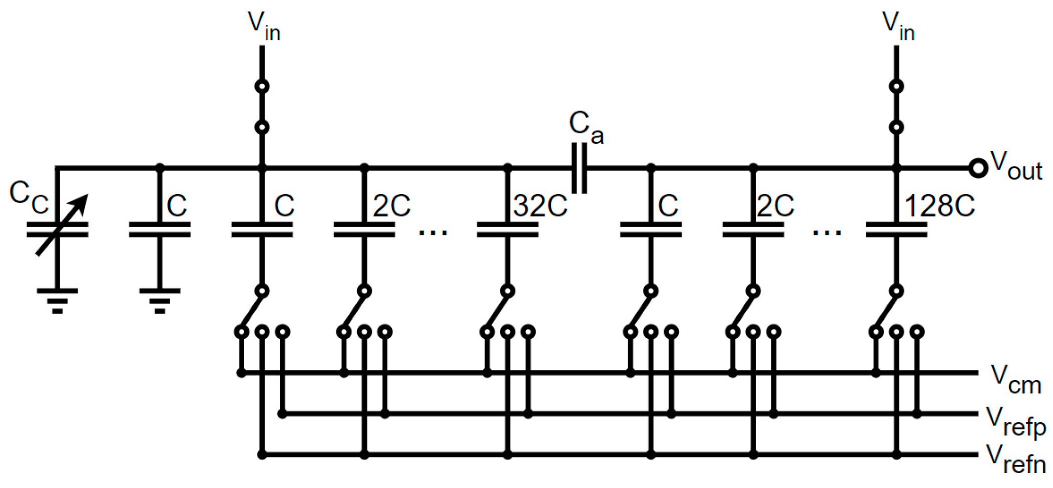
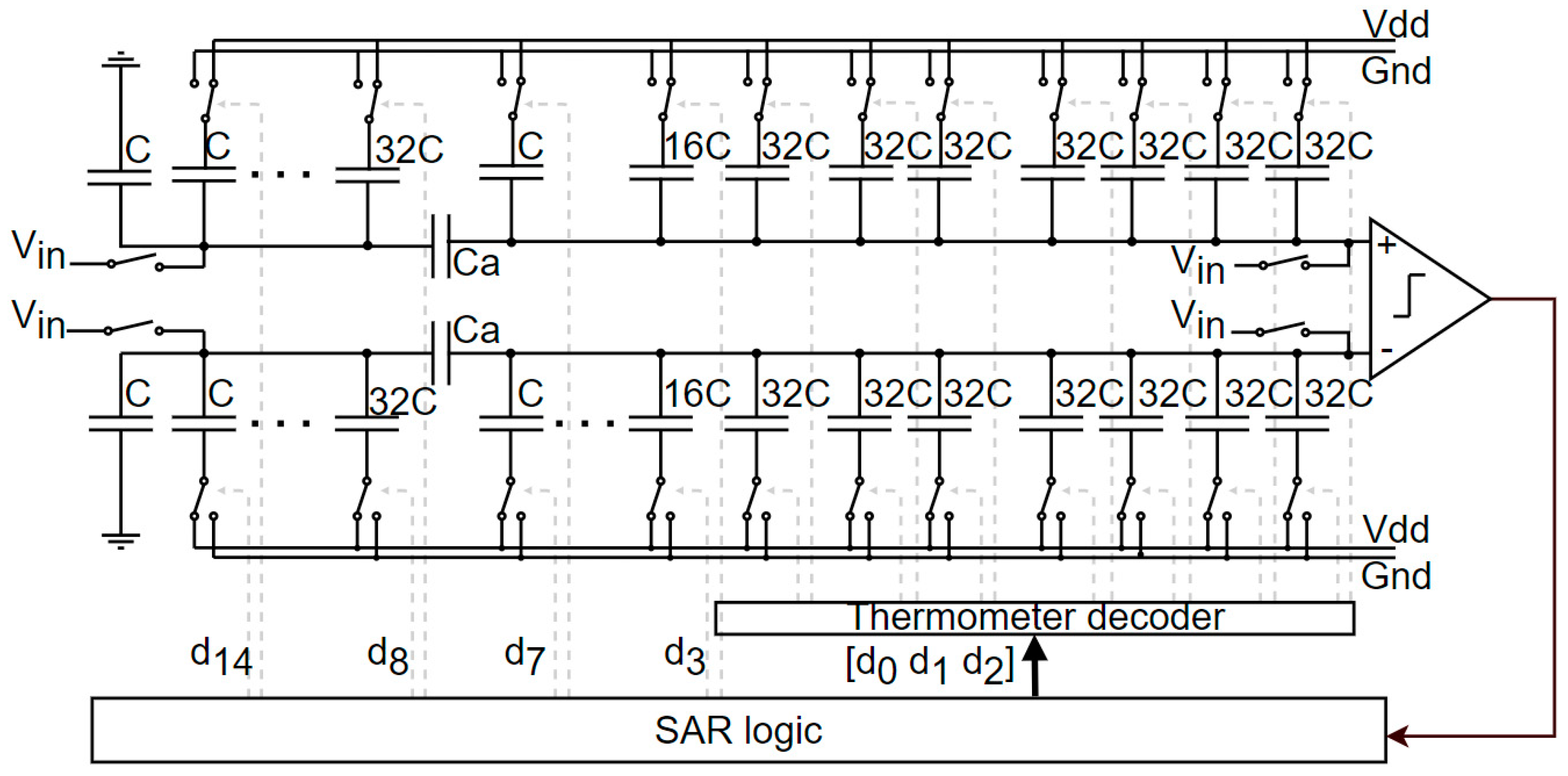
Figure 1 shows the proposed SAR ADC as well as the interdependence between blocks. In this paper, a 15-bit SAR ADC was considered as an example. Here, a capacitive digital-to-analog converter (C-DAC) was used, and the MSB and LSB segment sizes were, respectively, 8 and 6 bits, which provided a good trade-off between the chip area and linearity. When one introduces the common mode voltage into the processing, an additional intrinsic bit is found. The unit capacitor Cu is defined as 30 fF according to the kT/C noise requirements. Segmented DACs are well-known as a cause of non-linearities due to their high sensitivity to mismatch and also issues with parasitic capacitors. Hence, high-resolution converters must be calibrated. In this work, an automated calibration algorithm acting on a trimming capacitor was introduced. Additionally, a 3-bit dynamic element matching (DEM) algorithm was introduced to average distortions due to mismatch limitations. A classical comparator was considered. Finally, sampling was provided by a bootstrapped switch, which presented better linearity than a conventional switch.
2.2. Issues with a High-Resolution Capacitive DAC
To achieve a high resolution, classical C-DACs require a large array of capacitors. The size of these arrays increases exponentially with the number of bits, and the total sampling capacitor value of Cs is determined by thermal kT/C noise requirements. For some applications, the kT/C RMS noise () must be comparable to the quantization noise (LSB/). However, for other applications, the final SNR is less critical; hence, in the present design, we considered that a kT/C RMS noise of about LSB/3 should be sufficient. Equation (3) shows the sampling capacitor sizing resulting from this requirement:
Here, k corresponds to the Boltzmann constant, T is the temperature, and Cs is the sampling capacitor. Targeting a thermal noise of about LSB/3 in a 15-bit SAR ADC, the total sampling capacitor Cs must reach 10 pF. In our design, this requirement corresponds to choosing a unit capacitance, Cu, equal to 30 fF.
Figure 2 shows the simulation results for the noise model when a single-ended DAC architecture is considered. The sampling capacitor was sized to fit the noise distribution presented; thus, the Gaussian 6-sigma rule assumes that the noise level is within +/− 1 LSB, leading to an RMS value of about LSB/3.
In a differential scheme, the dynamic range for the signal doubles, meaning that the unit capacitor could be reduced accordingly without affecting the SNR.
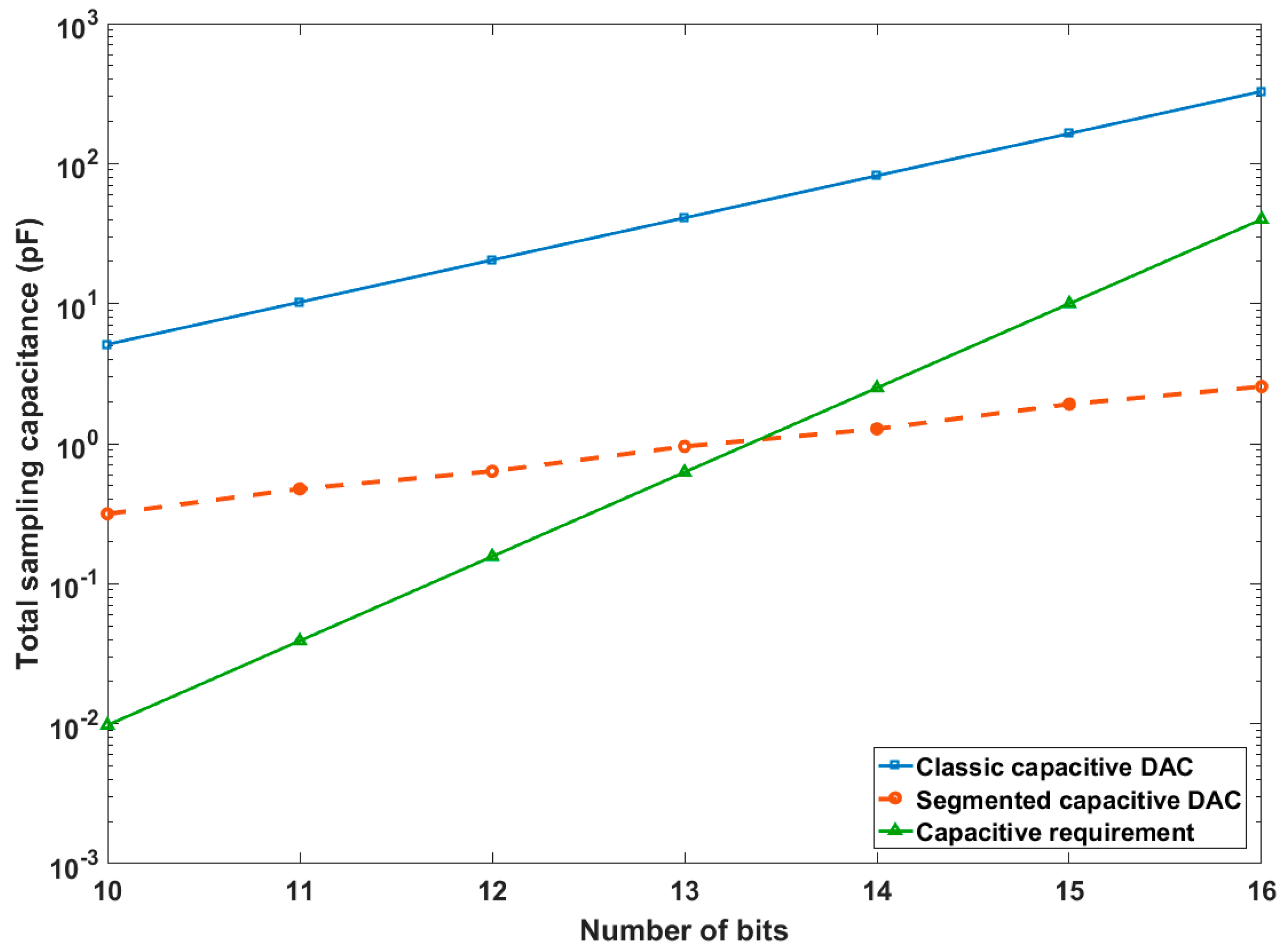
For a high-resolution design, after determining the total capacitor value following the kT/C noise rules, it is possible to calculate the value of the unit capacitor in the array. This value may be lower than the smallest capacitor available in the process design kits. One solution to this issue is to design specific MOM capacitors, which are smaller than those in process design kits [31]. In our design, we considered a segmented DAC scheme where the total number of capacitors in the DAC array was reduced.
Figure 2 shows the total DAC array capacitance that is necessary according to the kT/C thermal noise requirements (in green). Considering a unit capacitor of Cu = 5 fF, the blue curve shows the resultant value of the total capacitor for a classical non-segmented design. The red curve shows the total capacitor value considering a segmented DAC scheme with the same unit capacitor. In the segmented case, it appears that the value for the unit capacitor must be increased to reach the theoretical noise requirement (green curve).
Unfortunately, segmentation in the capacitor array leads to an extreme sensitivity to mismatch and parasitic capacitors. Due to its fractional value, the optimum for the bridge capacitor is not easily achievable. Consequently, the linearity in this architecture is very sensitive to capacitor mismatch. It is, therefore, necessary to compensate for these limitations by applying a calibration method. Some studies have proposed the use of a distinct digital foreground or background algorithm to perform this calibration, but this increases the digital complexity. In this study, we used an analog self-tuning technique.
3. Circuit Modelization
3.1. Capacitive C-DAC
The segmented architecture proposed in Figure 3 based on the Vmc switching architecture was divided into two segments: MSB on the right going to the output, and LSB on the left, separated by the bridge capacitor Ca. For improved linearity, we used more digits for the 8-bit MSB segment (from C to 128 C) than in the 6-bit LSB segment (from C to 32 C). The input signal was sampled on the top of these capacitors. The SAR voltage levels were generated by switching the reference voltages (VrefP, VrefN, and Vmc) over the bottom plate of these capacitors. A differential architecture was considered, but only one DAC is shown. In this scheme, an additional trimming capacitor Cc was considered to compensate for the mismatch error.
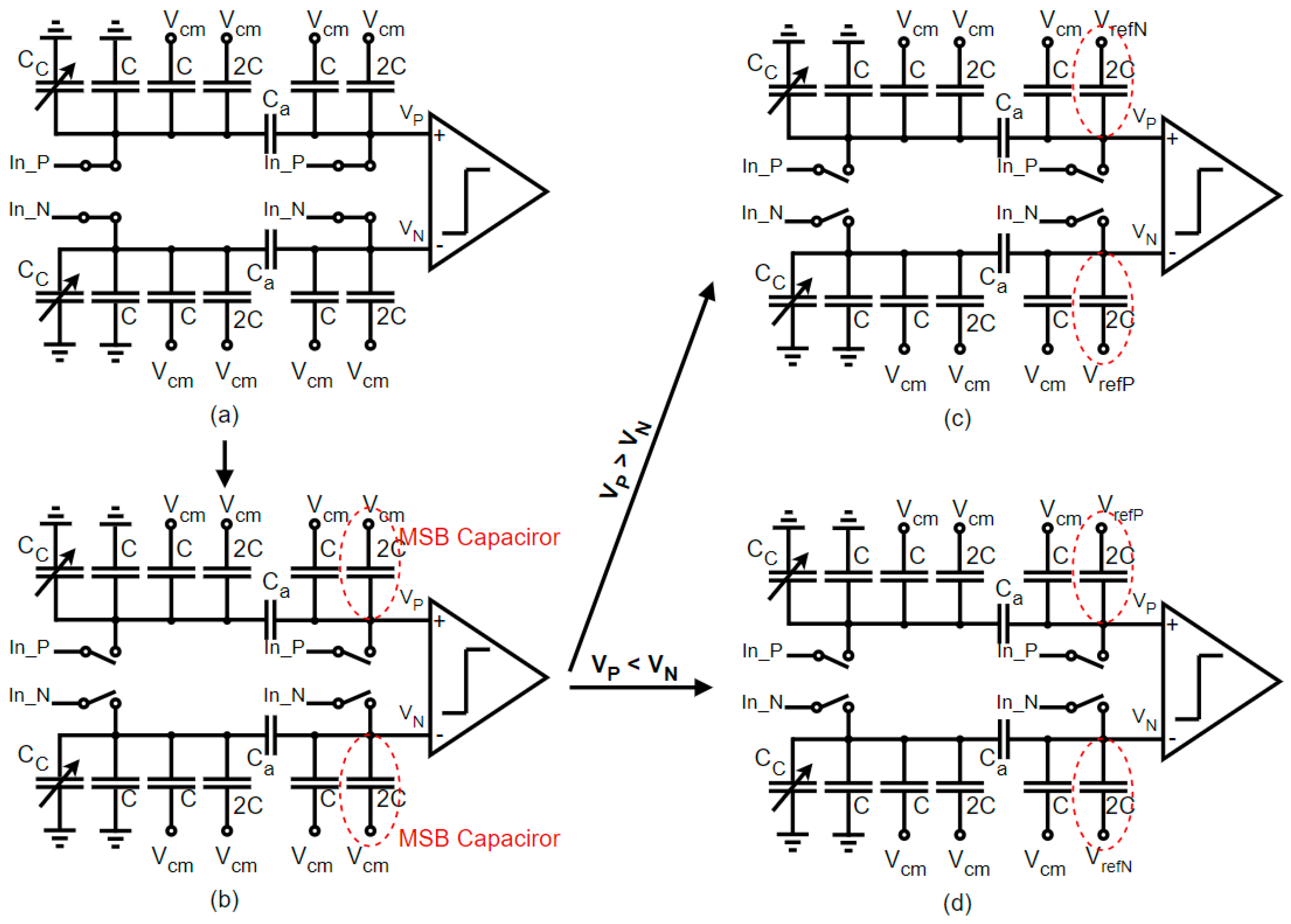
In Figure 4, we consider a simplified 4-bit converter as an example and describe the first steps of a Vmc-based switching algorithm [14,15]. The conversion process works as follows. During the sampling phase, the top plates of the capacitors were all connected to the input signal Vin while the bottom sides were connected to Vcm, as illustrated in Figure 4a. During the first conversion step illustrated in Figure 4b, if the comparison result was high (Vp > Vn), then the MSB capacitor 2C of the upper P-DAC performed a down transition (the level change operation was performed by switching the bottom plate from Vmc to VrefN). Symmetrically, the MSB capacitor 2C of the lower N-DAC performed an up transition (the bottom plate was switched from Vmc to VrefP), as shown in Figure 4c. Conversely, if the comparison result was low (Vp < Vn), the MSB capacitor of the P-DAC could be connected to VrefP, and the MSB capacitor of the N-DAC could be connected to VrefN, as illustrated in Figure 4d. Finally, the result of the comparison defines the MSB bit of the output digital code.
3.2. Mismatch Calibration
In a high-resolution segmented capacitor array, the non-binary value of the segmentation capacitor was a source of important non-linearity; hence, a mismatch compensation concept was required. Instead of using a fixed value for the capacitor Cc, we produced one that was variable and programmable. This trimming strategy was realized in order to compensate for the mismatch effect due to the bridge capacitor Ca. This concept is made consistent by oversizing the segmentation capacitor Ca and then linearly tuning the trimming capacitor Cc until the contribution from the LSB segment is equal to that of the MSB segment’s unit capacitor C. This trimming process was automated in our design.
Based on the notations illustrated in Figure 5, Equations (4) and (5) describe the two phases of charge redistribution. Here, the LSB equivalent capacitance is noted as CL, and the first seven MSB capacitances as CM. Ca is the bridge capacitor, and Cu is the unit capacitor.
The trimming capacitor Cc was calculated so that the output remained stable (). Equation (6) details the outcome result. The value chosen here for the unit capacitor Cu was 30 fF in order to fit the thermal noise limitations.
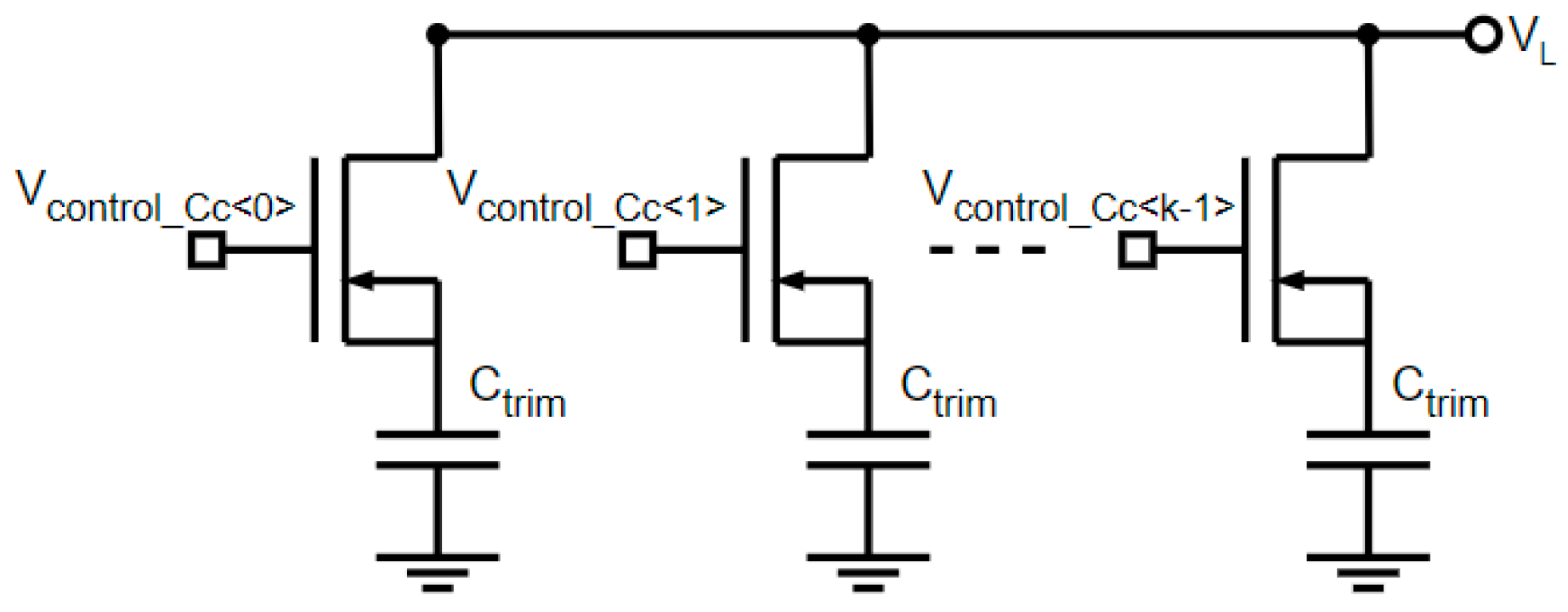
Figure 6 presents the set of trimming capacitors’ Cc architecture. This one is made up of a k-multiple capacitor Ctrim in parallel, which can be connected, or not, to the DAC network (node called VL in Figure 5) in order to modify the value of Cc. The digital tuning signal Vcontrol_Cc was determined by the calibration algorithm. After the calibration, the tuning capacitor Cc was determined through Equation (7).
Ideally, good matching means that the LSB segment presents the same contribution as the unit capacitor Cu in the MSB segment. However, if the bridge capacitor is oversized, the contribution of the LSB segment is greater than that of the unit capacitor. The progressive tuning of Cc can then be used to re-optimize matching in the circuit. This trimming process was automated in our design following the algorithm explained in reference [22]. The simplicity of this trimming method, along with the low surface that is consumed, is a major advantage compared to some other digital calibration methods.
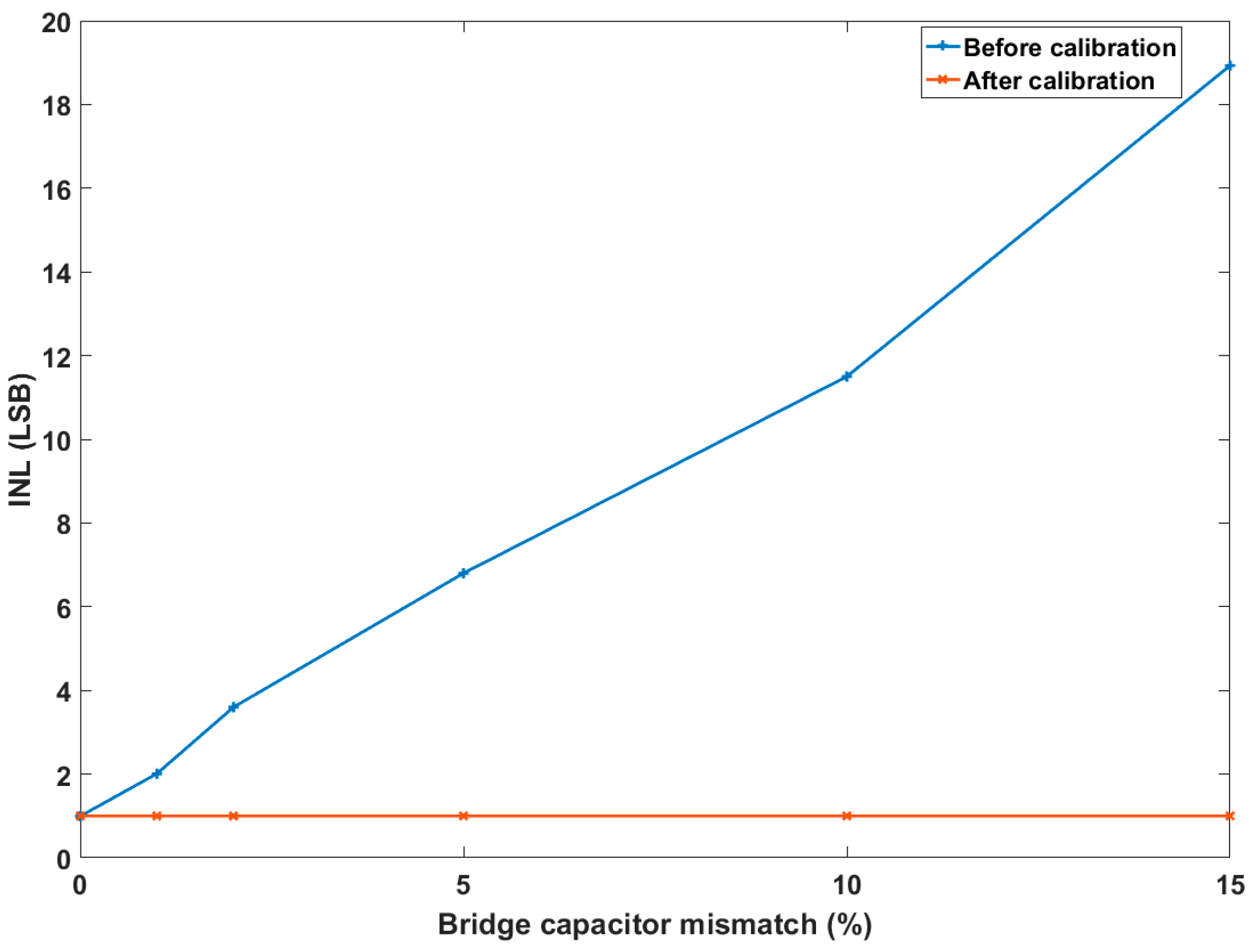
The calibration process was developed with a MATLAB model. The segmented DAC was assumed to be almost ideal; then, an additional random mismatch coefficient was applied to the segmentation capacitor alone. According to Monte Carlo simulations, the random coefficient follows a Gaussian distribution with a process-dependent standard deviation. The efficiency of the trimming can be observed through the strong reduction in integral non-linearity (INL) after calibration (Figure 7). The INL after calibration is equal to 1 LSB (INL of ideal ADC), and the mismatch of the bridge capacitor is fully balanced.
3.3. Partially Thermometer-Coded Capacitive Array
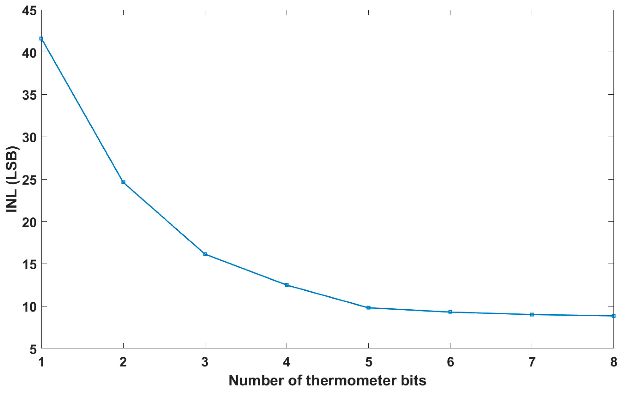
Thermometer coding was partially applied to our C-DAC array. Instead of binary elements, the DAC included some identical unary capacitors on the MSB side, with each bit split into identical parallel unit capacitors. The optimal result for the INL occurred for a fully thermometer-coded C-DAC. However, that would significantly increase the number of switches and, consequently, the decoder’s complexity, leading to a drastic increase in the circuit area. A possible compromise would be to include thermometer coding only for some of the first MSB bits. Figure 8 shows the ADC linearity versus the number of thermometer bits. One can observe that a 3-bit thermometer provides a good trade-off between the circuit area and linearity performance.
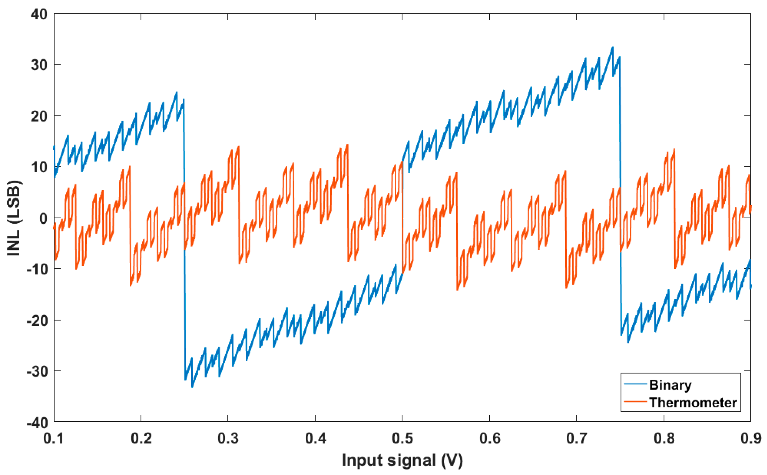
Figure 9 shows a 15-bit SAR ADC with a 3-bit thermometer-coded C-DAC. For this architecture, the SAR logic stands for a classic dichotomy logic circuit [32] before a thermometer decoder is added for the demultiplexing of the switch control [d0 d1 d3]. Figure 10 shows the modeled efficiency of a thermometer-coded C-DAC compared to a classical binary C-DAC when a significant mismatch effect following Pelgrom’s law [33] is included.
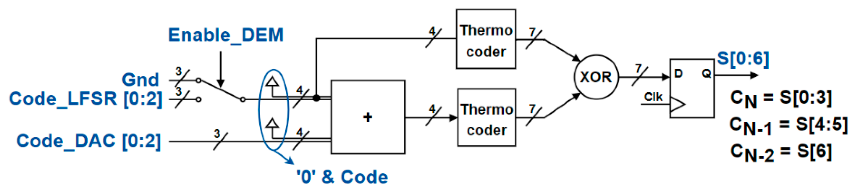
3.4. Dynamic Element Matching (DEM) Algorithm
A DEM is implemented over the thermometer-coded capacitive array. The algorithm exploits the non-uniform mismatch distribution to randomize the capacitor’s attribution [26]. In other words, bit bi is not always connected to the same capacitor but is instead connected to a random group of capacitors selected among the full arrays. For each conversion phase, the mismatch configuration is different. Therefore, the outcome INL is correlated to the mean value of a series of mismatches, and non-linearity gaps are reduced.
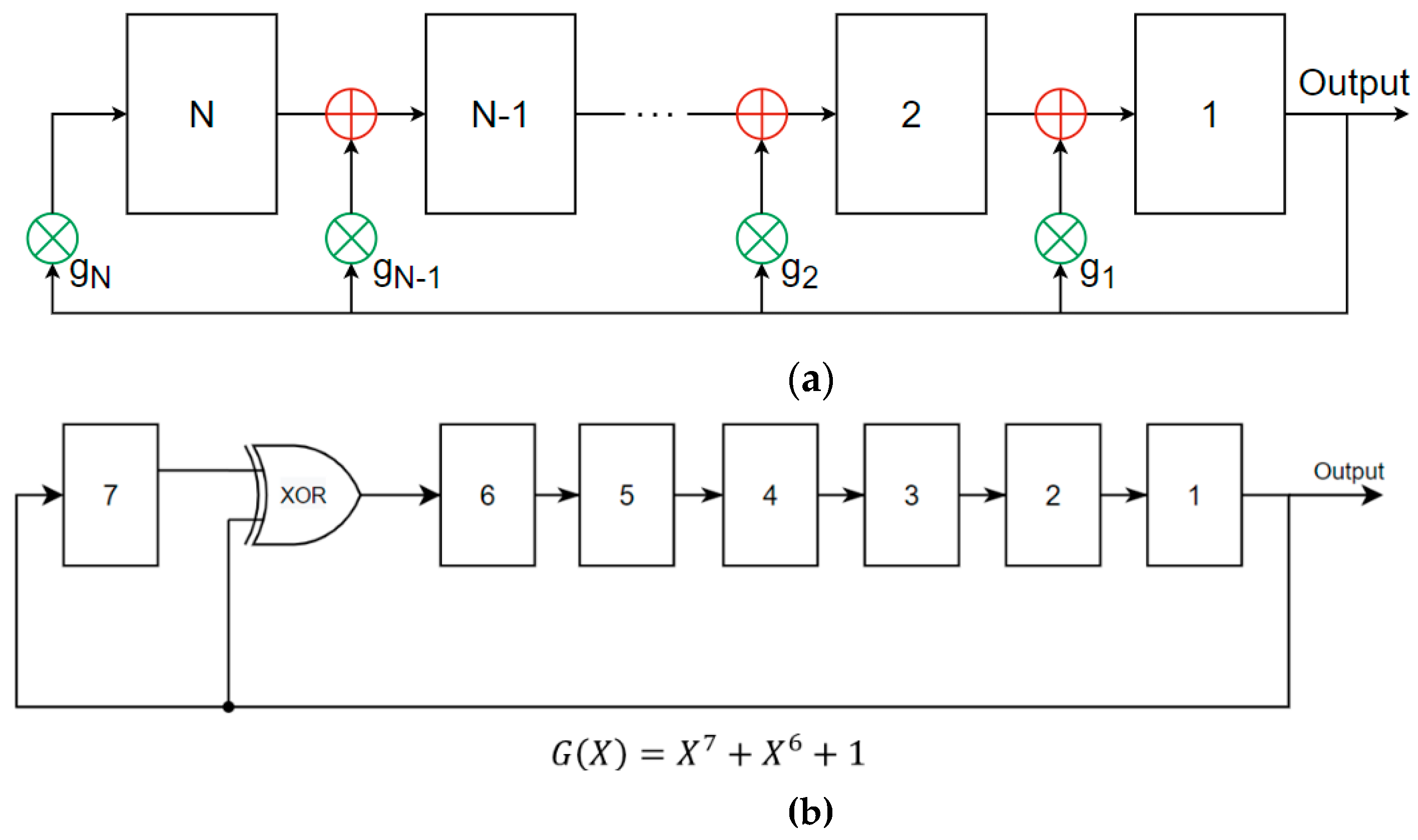
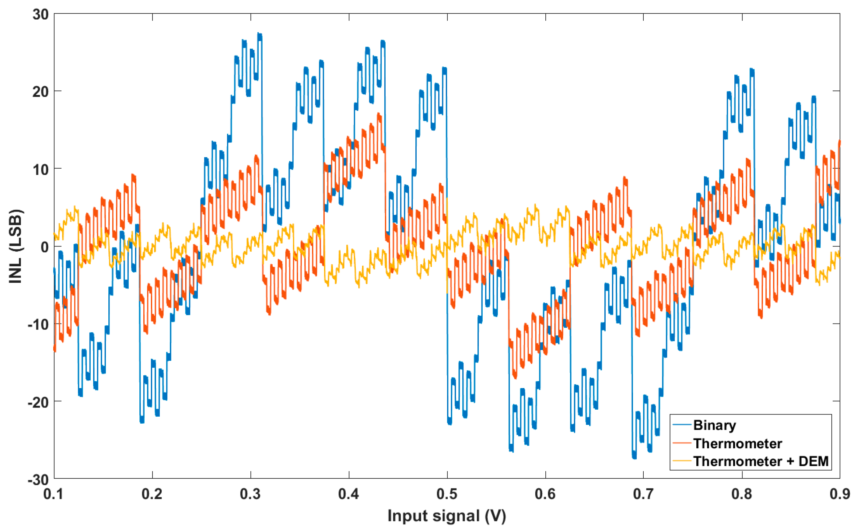
Ideally, DEM requires a random number generator. However, a digital pseudo-random number generator with a long-enough random cyclic sequence provides an adequate compromise. We used such a system, designed as shown in Figure 11. A linear feedback shift register (LFSR) was considered to generate the pseudo-random sequence, as illustrated in Figure 12. The polynomial order determines the sequence length, with the function applied based on (8). The technical efficiency could be observed through the strong reduction in INL after the application of DEM, considering a 2% mismatch for each unit capacitor, as shown in Figure 13 and Table 1.
Unfortunately, DEM suffers from the same limitations as a thermometer-coded DAC. The complexity and circuit area of these systems both increase strongly in line with the resolution. Hence, similar to the thermometer-coded DAC trade-off, in our design, the DEM was applied only over the first three MSB bits.
4. Noise Estimation
Usually, the SNR is calculated from the FFT measurement over several sinus periods. The SNR can be easily measured when the circuit is produced and tested. Unfortunately, when considering only simulation results, the data quantity needed for FFT calculation presents a critical issue. The following point can develop a faster SNR estimation methodology.
A second method consists of summing the various noise power contributions independently and then estimating the overall converter performance. The main limitation that was examined derived from the comparator input’s referred noise, the capacitive array’s kT/C thermal noise and noise from the reference buffers and (for the purposes of this study, the contribution of the power supply to the noise was not examined). The first noise estimation comes from the mathematical Equation (9). Each of these noise contributions was considered to follow a Gaussian distribution. To add all the noise contributions, the root sum square method was used.
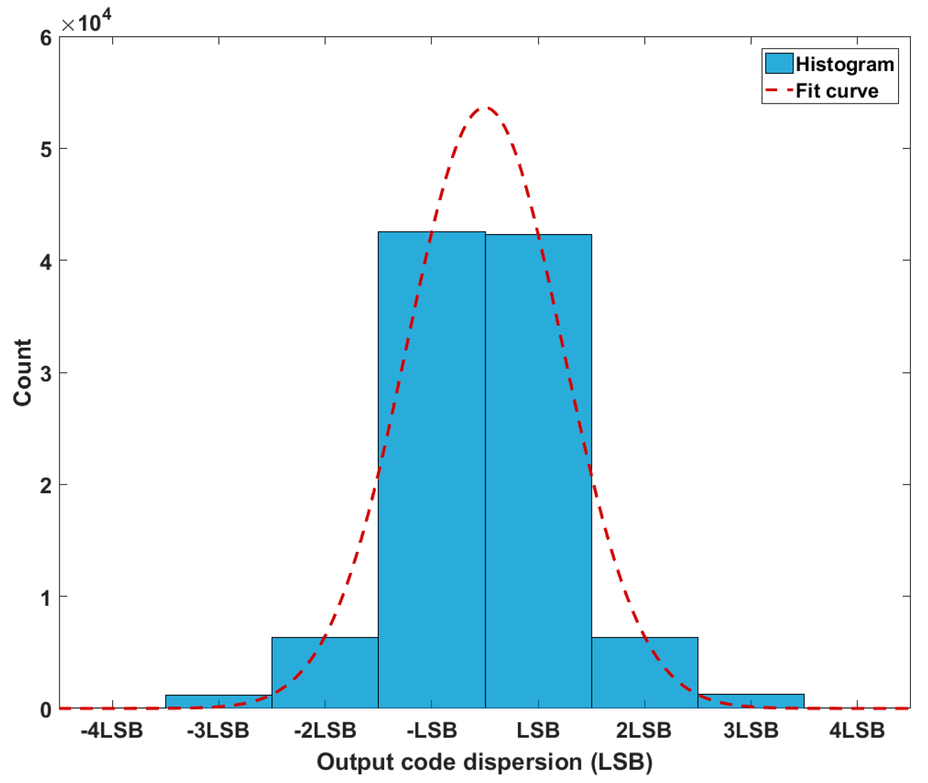
A third method for estimating the total noise is to consider the output code dispersion while processing a constant input signal in a transient noise domain. The standard deviation of the output codes’ dispersion that was obtained directly correlates with the total noise. Knowing the total noise level, the SNR was then obtained using mathematical calculus (10):
As an example, the comparator noise can be considered around 0.82 LSB, the kT/C noise around 0.22 LSB, and other noise contributions to be null. The conversion of a sine wave and FFT calculation regarding our MATLAB model provided an SNR of 82.98 dB, which corresponds to a total noise of about 0.822 LSB. The second method, using Equation (9), allowed a mathematical estimation of about 0.849 LSB. Finally, Figure 14 displays the simulated output code dispersion for a 600.03 mV constant input. The standard deviation of the output code dispersion was about 0.83 LSB, whereas, considering Equation (9), was about 0.85 LSB.
These three methods have been simulated over different noise configurations, and the results converge to the same noise estimation for each test. Thus, the second and third methods allowed for a simple and fast noise estimation during the design phase without resorting to the FFT calculation, which requires a large number of samples.
5. Conclusions
In this paper, we propose a methodology for a high-resolution differential SAR ADC based on a segmented C-DAC. The method we present combines an automated mismatch calibration technique based on a trimming capacitor and a DEM algorithm that is applicable on thermometer-coded C-DAC to achieve a high resolution and compensate for mismatch errors while, at the same time, reducing the chip area. In addition, a MATLAB model was presented to illustrate the efficiency of the proposed algorithms. Thus, embedding these two algorithms simultaneously allows for a reduction in the worst-case INL from 28 LSB to 6 LSB when a mismatch of 2% is applied to each unit capacitor.
Secondly, a simple method for estimating the noise is presented. It is based on two fast simulations, owing to a mathematical equation applied to each noise source or the consideration of the output codes’ dispersion after a limited amount of simulation data. These two methods were in good agreement with the usual FFT method when applied to a MATLAB model. These methods make it possible to quickly estimate the SNR for an ADC during the design simulation phase without FFT processing, which, for a high-resolution converter, would require a significant amount of data.
Finally, Table 2 presents the performance of SAR ADCs published in ISSCC and VLSI between 2017 and 2022. This represents so far the state of the art as described in [34]. In comparison to our ADC simulation results, the table firstly highlights the low power consumption results where we expect a total power dissipation of 30µW, including all contributing sources (DAC, comparators, switches, reference voltage, digital control, etc.). Secondly, from the SNR point of view, we listed the SNR as expected by front-end simulation using the method explained in Section 4. In terms of FOM, the expected performance for our ADC closely gets to the state of the art measurement results for a comparable resolution and technology node, except for [35]. At last, although not presented in the table, the differentiating feature for our ADC solution arises from die area occupation, which is expected to be intrinsically very small due to the use of a segmented DAC architecture.
Author Contributions
Conceptualization, W.B. and D.D.; methodology, W.B. and D.D.; writing—original draft preparation, W.B.; writing—review and editing supervision, D.D.; project administration, D.D. All authors have read and agreed to the published version of the manuscript.
Funding
This research received no external funding.
Data Availability Statement
Data is contained within the article.
Conflicts of Interest
The authors declare no conflict of interest.
References
- McCreary, J.L.; Gray, P.R. All-MOS charge redistribution analog-to-digital conversion techniques. IEEE J. Solid-State Circuits 1975, 10, 371–379. [Google Scholar] [CrossRef]
- Saberi, M.; Lotfi, R. Segmented Architecture for Successive Approximation Analog-to-Digital Converters. IEEE Trans. Very Large Scale Integr. (VLSI) Syst. 2014, 22, 593–606. [Google Scholar] [CrossRef]
- Scott, M.D.; Boser, B.E.; Pister, K.S.J. An ultralow-energy adc for smart dust. IEEE J. Solid-State Circuits 2003, 38, 1123–1129. [Google Scholar] [CrossRef]
- Lee, S.-K.; Park, S.-J.; Park, H.-J.; Sim, J.-Y. A 21 fJ/Conversion-Step 100 kS/s 10-bit ADC With a Low-Noise Time-Domain Comparator for Low-Power Sensor Interface. IEEE J. Solid-State Circuits 2011, 46, 651–659. [Google Scholar] [CrossRef]
- Zou, X.; Xu, X.; Yao, L.; Lian, Y. A 1-V 450-nW Fully Integrated Programmable Biomedical Sensor Interface Chip. IEEE J. Solid-State Circuits 2009, 44, 1067–1077. [Google Scholar]
- Ginsburg, B.P.; Chandrakasan, A.P. 500-MS/s 5-bit ADC in 65-nm CMOS With Split Capacitor Array DAC. IEEE J. Solid-State Circuits 2007, 42, 739–747. [Google Scholar] [CrossRef]
- Saul, P.H. Successive approximation analog-to-digital conversion at video rates. IEEE J. Solid-State Circuits 1981, 16, 147–151. [Google Scholar] [CrossRef]
- Yang, Z.; Van der Spiegel, J. A 10-bit 8.3MS/s switched-current successive approximation ADC for column-parallel imagers. In Proceedings of the 2008 IEEE International Symposium on Circuits and Systems (ISCAS), Seattle, WA, USA, 18–21 May 2008; pp. 224–227. [Google Scholar]
- Mortezapour, S.; Lee, E.K.F. A 1-V, 8-bit successive approximation ADC in standard CMOS process. IEEE J. Solid-State Circuits 2000, 35, 642–646. [Google Scholar] [CrossRef]
- Klimach, H.; Schneider, M.; Galup-Montoro, C. An M-2M digital-to-analog converter design methodology based on a physical mismatch model. In Proceedings of the 2008 IEEE International Symposium on Circuits and Systems (ISCAS), Seattle, WA, USA, 18–21 May 2008. [Google Scholar]
- Lin, C.-S.; Liu, B.-D. A new successive approximation architecture for low-power low-cost CMOS A/D converter. IEEE J. Solid-State Circuits 2003, 38, 54–62. [Google Scholar]
- Hong, X.; Yang, C.; Zhang, X. An energy-efficient SAR ADC with a partial-monotonic capacitor switching technique. In Proceedings of the IEEE 2nd Advanced Information Technology, Electronic and Automation Control Conference, Chongqing, China, 25–26 March 2017; pp. 2050–2054. [Google Scholar]
- Tung, W.; Huang, S.-C. An Energy-Efficient 11-bit 10-MS/s SAR ADC with Monotonie Switching Split Capacitor Array. In Proceedings of the 2008 IEEE International Symposium on Circuits and Systems (ISCAS), Seattle, WA, USA, 18–21 May 2008; pp. 1–5. [Google Scholar]
- Hsieh, S.-E.; Hsieh, C.-C. A 0.3-V 0.705-fJ/Conversion-Step 10-bit SAR ADC With a Shifted Monotonic Switching Procedure in 90-nm CMOS. IEEE Trans. Circuits Syst. II 2016, 63, 1171–1175. [Google Scholar] [CrossRef]
- Li, L.; Liu, D.; Lei, W.; Hu, Y.; Zou, X.; Li, D. A low power charge-redistribution SAR ADC with a monotonic switching procedure. In Proceedings of the IEEE International Conference on Solid-State and Integrated Circuit Technology, Guilin, China, 28–31 October 2014; pp. 1–3. [Google Scholar]
- Um, J.-Y.; Kim, Y.-J.; Song, E.-W.; Sim, J.-Y.; Park, H.-J. A Digital-Domain Calibration of Split-Capacitor DAC for a Differential SAR ADC Without Additional Analog Circuits. IEEE Trans. Circuits Syst. I 2013, 60, 2845–2856. [Google Scholar] [CrossRef]
- Chung, Y.-H.; Hu, C.-Y.; Chang, C.-W. A 38-mW 7-bit 5-GS/s Time-Interleaved SAR ADC with Background Skew Calibration. In Proceedings of the 2018 IEEE Asian Solid-State Circuits Conference (A-SSCC), Tainan, Taiwan, 5–7 November 2018; pp. 243–246. [Google Scholar]
- Fan, H.; Wang, Y.; Wu, X. A Realizable Digital Bubble Sorting SAR ADC Calibration Technology. In Proceedings of the 2021 International Conference on IC Design and Technology (ICICDT), Dresden, Germany, 15–17 September 2021; pp. 1–4. [Google Scholar]
- Dai, S.; Hu, K.; Rosenstein, J.K. A Segmented SAR/SS ADC with Digital Error Correction and Programmable Resolution for Column-Parallel Sensor Arrays. In Proceedings of the 2020 IEEE International Symposium on Circuits and Systems (ISCAS), Seville, Spain, 12–14 October 2020; pp. 1–5. [Google Scholar]
- Wu, J.; Wu, J. Background Calibration of Capacitor Mismatch and Gain Error in Pipelined-SAR ADC Using Partially Split Structure. In Proceedings of the 2021 IEEE 5th Advanced Information Technology, Electronic and Automation Control Conference (IAEAC), Chongqing, China, 12–14 March 2021; pp. 1882–1885. [Google Scholar]
- McNeill, J.; Coln, M.C.W.; Larivee, B.J. Split ADC” Architecture for Deterministic Digital Background Calibration of a 16-bit 1-MS/s ADC. IEEE J. Solid-State Circuit 2005, 40, 12. [Google Scholar] [CrossRef]
- Chen, Y.; Zhu, X.; Tamura, H.; Kibune, M.; Tomita, Y.; Hamada, T.; Yoshioka, M.; Ishikawa, K.; Takayama, T.; Ogawa, J.; et al. Split capacitor DAC mismatch calibration in successive approximation ADC. IEICE Trans. Electron. 2010, 93, 295–302. [Google Scholar] [CrossRef]
- Liu, K.; Du, Z.; Shao, L.; Ma, X. A trimming technique for capacitive SAR ADC as sensor interface. J. Semicond. 2015, 36, 125004. [Google Scholar] [CrossRef]
- Thirunakkarasu, S.; Bakkaloglu, B. Built-in Self-Calibration and Digital-Trim Technique for 14-Bit SAR ADCs Achieving ±1 LSB INL. IEEE Trans. Very Large Scale Integr. (VLSI) Syst. 2015, 23, 916–925. [Google Scholar] [CrossRef]
- Bialek, J.; Wickmann, A.; Ohnhaeuser, F.; Fischer, G.; Weigel, R.; Ussmueller, T. Implementation of a digital trim scheme for SAR ADCs. Adv. Radio Sci. 2013, 11, 227–230. [Google Scholar] [CrossRef] [Green Version]
- Gallin-Martel, L.; Dzahini, D.; Hostachy, J.-Y.; Rarbi, F.; Rossetto, O. Design of High Dynamic Range Digital to Analog Converters for the Calibration of the CALICE Si-W Ecal readout electronics. In Proceedings of the Topical Workshop on Electronics for Particle Physics 2009, Paris, France, 21–25 September 2009; pp. 127–131. [Google Scholar]
- Haenzsche, S. Analysis of a charge redistribution SAR ADC with partially thermometer coded DAC. In Proceedings of the 2013 European Conference on Circuit Theory and Design (ECCTD), Dresden, Germany, 8–12 September 2013; pp. 1–4. [Google Scholar]
- Xie, L.; Han, X.; Zhang, H.; Jin, X. A 12bit 16MS/s Asynchronous SAR ADC with Speed-Enhanced Comparator and TSPC Latch. In Proceedings of the IEEE 4th International Conference on Integrated Circuits and Microsystems, Beijing, China, 25–27 October 2019; pp. 104–108. [Google Scholar]
- Li, W.; Li, F.; Liu, J.; Li, H.; Wang, Z. A 13-bit 160MS/s pipelined subranging-SAR ADC with low-offset dynamic comparator. In Proceedings of the IEEE Asian Solid-State Circuits Conference, Seoul, Republic of Korea, 6–8 November 2017; pp. 225–228. [Google Scholar]
- Bandla, K.; Harikrishnan, A.; Pal, D. Design of Low Power, High Speed, Low Offset and Area Efficient Dynamic-Latch Comparator for SAR-ADC. In Proceedings of the International Conference on Innovative Trends in Communication and Computer Engineering, Aswan, Egypt, 8–9 February 2020; pp. 299–302. [Google Scholar]
- Chen, N.; Chou, P.; Graeb, H.; Lin, M. High-Dentsity MOM Capacitor Array with Novel Mortise-Tenon Structure for Low-Power SAR-ADC. In Proceedings of the IEEE Design, Automation and Test in Europe, Lausanne, Switzerland, 27–31 March 2017. [Google Scholar]
- Zhu, Y.; Chan, C.-H.; Chio, U.-F.; Sin, S.-W.; Seng-Pan, U.; Martins, R.P.; Maloberti, F. A 10-bit 100-MS/s Reference-Free SAR ADC in 90 nm CMOS. IEEE J. Solid-State Circuits 2010, 45, 1111–1121. [Google Scholar] [CrossRef]
- Sheikholeslami, A. Process Variation and Pelgrom’s Law [Circuit Intuitions]. IEEE Solid-State Circuits Mag. 2015, 7, 8–9. [Google Scholar] [CrossRef]
- Murmann, B. ADC Performance Survey 1997–2022. Available online: https://github.com/bmurmann/ADC-survey (accessed on 15 January 2020).
- Choo, K.; An, H.; Sylvester, D.; Blaauw, D. 14.1-ENOB 184.9dB-FoM Capacitor-Array-Assisted Cascaded Charge-Injection SAR ADC. In Proceedings of the 2021 IEEE International Solid-State Circuits Conference (ISSCC), San Francisco, CA, USA, 13–22 February 2021; pp. 372–374. [Google Scholar]
- Xu, H.; Cai, Y.; Du, L.; Zhou, Y.; Xu, B.; Gong, D.; Ye, J.; Chiu, Y. 28.6 A 78.5dB-SNDR radiation- and metastability-tolerant two-step split SAR ADC operating up to 75MS/s with 24.9mW power consumption in 65nm CMOS. In Proceedings of the 2017 IEEE International Solid-State Circuits Conference (ISSCC), San Francisco, CA, USA, 5–9 February 2017; pp. 476–477. [Google Scholar]
- Lee, J.; Lee, K.R.; Eovino, B.E.; Park, J.H.; Lin, L.; Yoo, H.J.; Yoo, J. 11. 1 A 5.37mW/Channel Pitch-Matched Ultrasound ASIC with Dynamic-Bit-Shared SAR ADC and 13.2V Charge-Recycling TX in Standard CMOS for Intracardiac Echocardiography. In Proceedings of the 2019 IEEE International Solid-State Circuits Conference (ISSCC), San Francisco, CA, USA, 17–21 February 2019; pp. 190–192. [Google Scholar]
- Liu, J.; Tang, X.; Zhao, W.; Shen, L.; Sun, N. 16.5 A 13b 0.005mm2 40MS/s SAR ADC with kT/C Noise Cancellation. In Proceedings of the 2020 IEEE International Solid-State Circuits Conference (ISSCC), San Francisco, CA, USA, 16–20 February 2020; pp. 258–260. [Google Scholar]
- Kiene, G.; Catania, A.; Overwater, R.; Bruschi, P.; Charbon, E.; Babaie, M.; Sebastiano, F. A 1GS/s 6-to-8b 0.5mW/Qubit Cryo-CMOS SAR ADC for Quantum Computing in 40nm CMOS. In Proceedings of the 2021 IEEE International Solid-State Circuits Conference (ISSCC), San Francisco, CA, USA, 13–22 February 2021; pp. 214–216. [Google Scholar]
- Tang, X.; Shen, Y.; Xin, X.; Liu, S.; Cai, J.; Zhu, Z.; Sun, N. A 10-Bit 100-MS/s SAR ADC with Always-on Reference Ripple Cancellation. In Proceedings of the IEEE Symposium on VLSI Circuits, Honolulu, HI, USA, 16–19 June 2020; pp. 1–2. [Google Scholar]
- Li, Z.; Dutta, A.; Mukherjee, A.; Tang, X.; Shen, L.; He, L.; Sun, N. A SAR ADC with Reduced kT/C Noise by Decoupling Noise PSD and BW. In Proceedings of the IEEE Symposium on VLSI Circuits, Honolulu, HI, USA, 16–19 June 2020; pp. 1–2. [Google Scholar]
- Hung, P.D.; Park, Y.; Kweon, S.-J.; Lee, T.; Jeon, H.; Koh, S.-T.; Cho, I.; Yoon, J.-B.; Park, I.; Kim, C.; et al. A Self-Powered Wireless Gas Sensor Node Based on Photovoltaic Energy Harvesting. In Proceedings of the Symposium on VLSI Circuits, Kyoto, Japan, 13–19 June 2021; pp. 1–2. [Google Scholar]
- Lee, J.; Lim, Y.; Lee, J.; Jang, T.; Kang, K.; Cho, J.; Oh, S.; Lee, J. A 0.56mW 63.6dB SNDR 250MS/s SAR ADC in 8nm FinFET. In Proceedings of the 2022 IEEE Symposium on VLSI Technology and Circuits, Honolulu, HI, USA, 12–17 June 2022; pp. 90–92. [Google Scholar]
- Chen, R.; Wang, H.; Chandrakasan, A.; Lee, H.-S. RaM-SAR: A Low Energy and Area Overhead, 11.3fJ/conv.-step 12b 25MS/s Secure Random-Mapping SAR ADC with Power and EM Side-channel Attack Resilience. In Proceedings of the 2022 IEEE Symposium on VLSI Technology and Circuits, Honolulu, HI, USA, 12–17 June 2022; pp. 94–95. [Google Scholar]
Figure 1.
Proposed SAR ADC architecture diagram.

Figure 2.
Total capacitance for a non-segmented or segmented DAC, and the optimum requirements to limit kT/C noise.
Figure 2.
Total capacitance for a non-segmented or segmented DAC, and the optimum requirements to limit kT/C noise.

Figure 3.
Segmented C-DAC architecture based on Vmc switching algorithm.

Figure 4.
First steps of this SAR switching algorithm in a limited 4-bit example. (a) Sampling phase; (b) First comparison; (c) Second comparison if b0 = 1; (d) Second comparison if b0 = 0.
Figure 4.
First steps of this SAR switching algorithm in a limited 4-bit example. (a) Sampling phase; (b) First comparison; (c) Second comparison if b0 = 1; (d) Second comparison if b0 = 0.

Figure 5.
Illustration of the calibration algorithm.

Figure 6.
Trimming capacitor array.

Figure 7.
INL simulation results, before and after calibration when a mismatch was applied to the segmentation bridge capacitor alone.
Figure 7.
INL simulation results, before and after calibration when a mismatch was applied to the segmentation bridge capacitor alone.

Figure 8.
ADC linearity versus the number of thermometer bits.

Figure 9.
Diagram of our 15-bit ADC with 3-bit thermometer coding.

Figure 10.
ADC INL for classical and thermometer-coded C-DAC.

Figure 11.
A 3-bit DEM architecture.

Figure 12.
(a) Nth-order polynomial generation and (b) example of seventh-order polynomial implementation.
Figure 12.
(a) Nth-order polynomial generation and (b) example of seventh-order polynomial implementation.

Figure 13.
INL simulations using MATLAB for a 15-bit thermometer-coded C-DAC with and without DEM.

Figure 14.
Output code dispersion for a 600.03 mV input.


Table 1.
ADC performance summary considering a 2% mismatch for each unit capacitor.
| Architecture | INL |
|---|---|
| Binary C-DAC | ±28 LSB |
| Thermometer C-DAC | ±18 LSB |
| Thermometer C-DAC + DEM | ±6 LSB |
Table 2.
ADC performance summary and comparison.
| Reference | Technology (nm) | Resolution (bits) | Sampling Rate (MS/s) | SNDR (dB) | Total Power (µW) | FOM (fJ/Conv-step) |
|---|---|---|---|---|---|---|
| [35] | 180 | 17 | 0.006 | 86.7 | 0.468 | 4.4 |
| [36] | 65 | 14 | 75 | 70.8 | 24,900 | 116.8 |
| [37] | 180 | 10 | 20 | 56.9 | 1230 | 107.2 |
| [38] | 40 | 13 | 40 | 69 | 591 | 6.4 |
| [39] | 40 | 8 | 900 | 33.4 | 700 | 20.3 |
| [40] | 40 | 10 | 100 | 56.3 | 1400 | 26.1 |
| [41] | 40 | 12 | 12 | 59.6 | 472 | 50.2 |
| [42] | 180 | 10 | 0.001 | 57.7 | 0.204 | 324.2 |
| [43] | 8 | 12 | 250 | 62 | 560 | 2.2 |
| [44] | 65 | 12 | 25 | 67.5 | 547 | 11.2 |
| This work | 65 | 15 | 0.2 | (SNR *)79.9 | 30 | 18.5 |
* This SNR comes from simulations, following the method explained in Section 4.
Disclaimer/Publisher’s Note: The statements, opinions and data contained in all publications are solely those of the individual author(s) and contributor(s) and not of MDPI and/or the editor(s). MDPI and/or the editor(s) disclaim responsibility for any injury to people or property resulting from any ideas, methods, instructions or products referred to in the content. |
© 2023 by the authors. Licensee MDPI, Basel, Switzerland. This article is an open access article distributed under the terms and conditions of the Creative Commons Attribution (CC BY) license (https://creativecommons.org/licenses/by/4.0/).
Share and Cite
MDPI and ACS Style
Bontems, W.; Dzahini, D. Methodology for a Low-Power and Low-Circuit-Area 15-Bit SAR ADC Using Split-Capacitor Mismatch Compensation and a Dynamic Element Matching Algorithm. Chips 2023, 2, 31-43. https://doi.org/10.3390/chips2010003
AMA Style
Bontems W, Dzahini D. Methodology for a Low-Power and Low-Circuit-Area 15-Bit SAR ADC Using Split-Capacitor Mismatch Compensation and a Dynamic Element Matching Algorithm. Chips. 2023; 2(1):31-43. https://doi.org/10.3390/chips2010003
Chicago/Turabian StyleBontems, William, and Daniel Dzahini. 2023. "Methodology for a Low-Power and Low-Circuit-Area 15-Bit SAR ADC Using Split-Capacitor Mismatch Compensation and a Dynamic Element Matching Algorithm" Chips 2, no. 1: 31-43. https://doi.org/10.3390/chips2010003