
Materials Based on Amorphous Al2O3 and Composite W-Al2O3 for Solar Coatings Deposited by High-Rate Sputter Processes
 , ,
, ,
Abstract
:1. Introduction
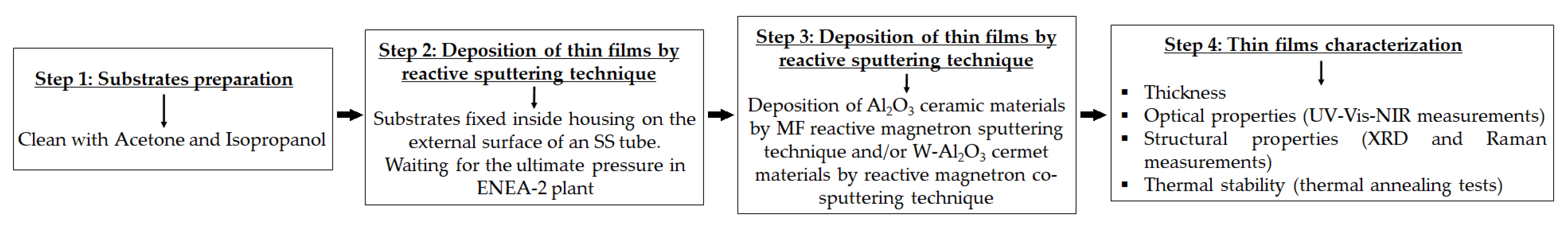
2. Experimental Section
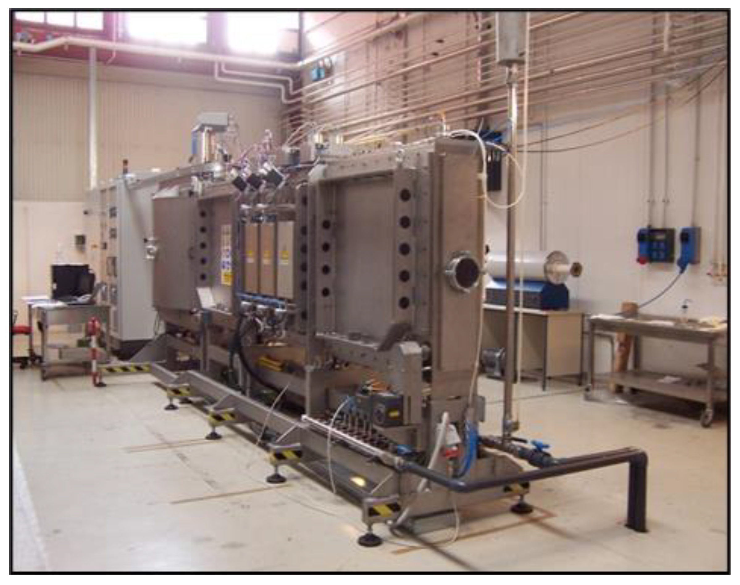
2.1. Magnetron Sputtering System
2.2. Materials Preparation
2.3. Materials Characterization
3. Results and Discussion
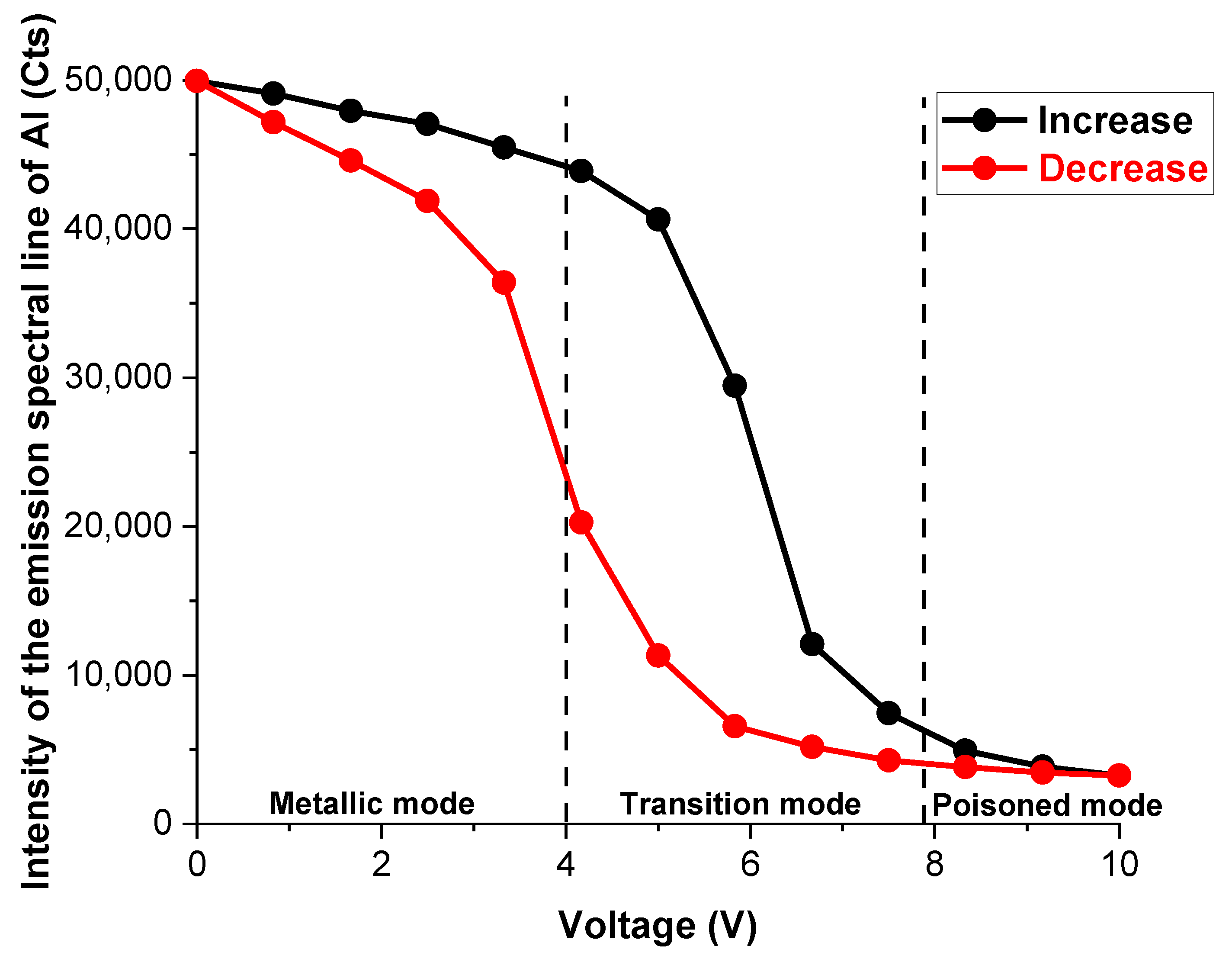
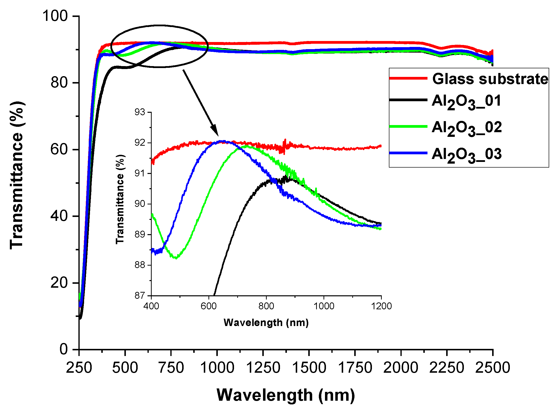
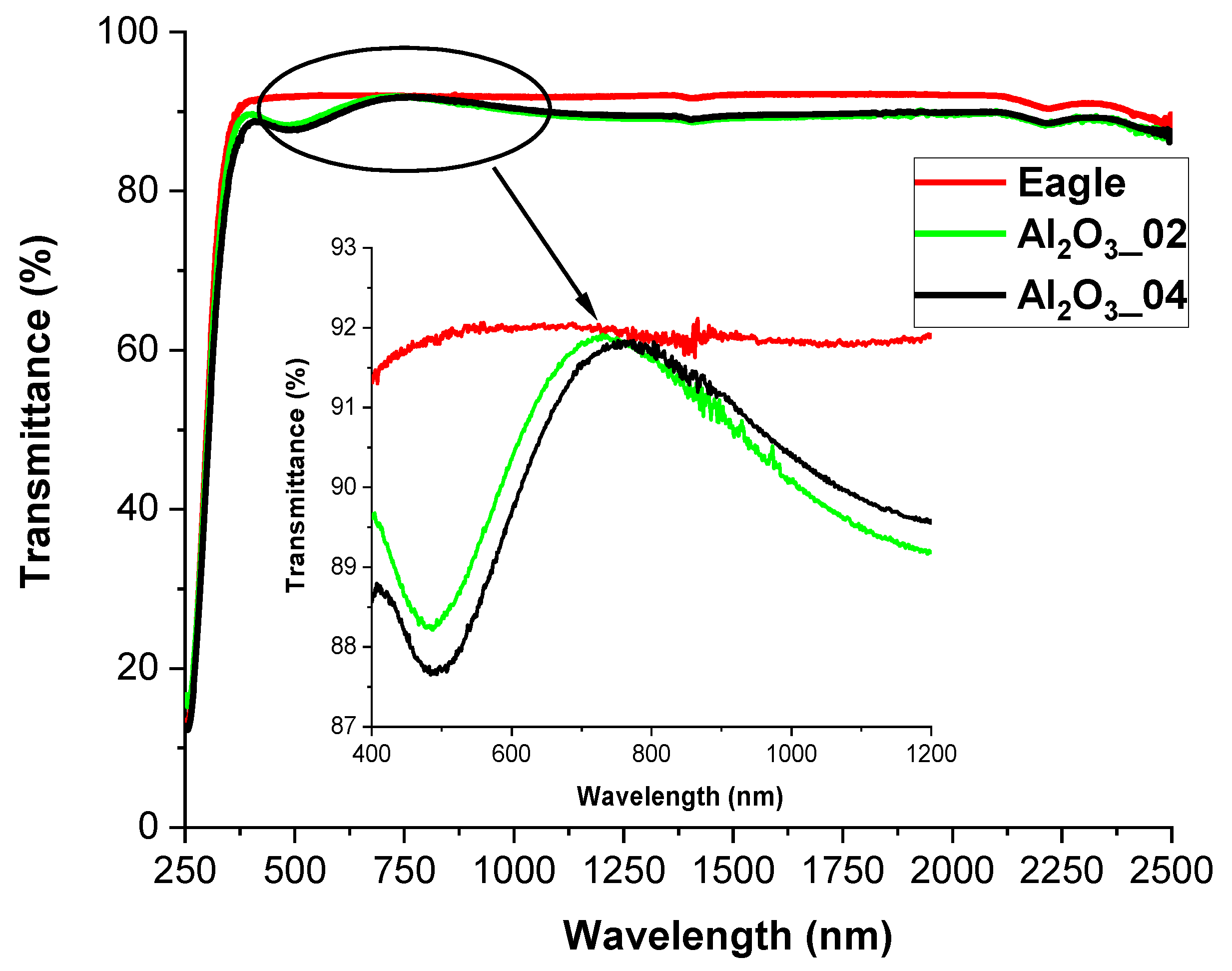
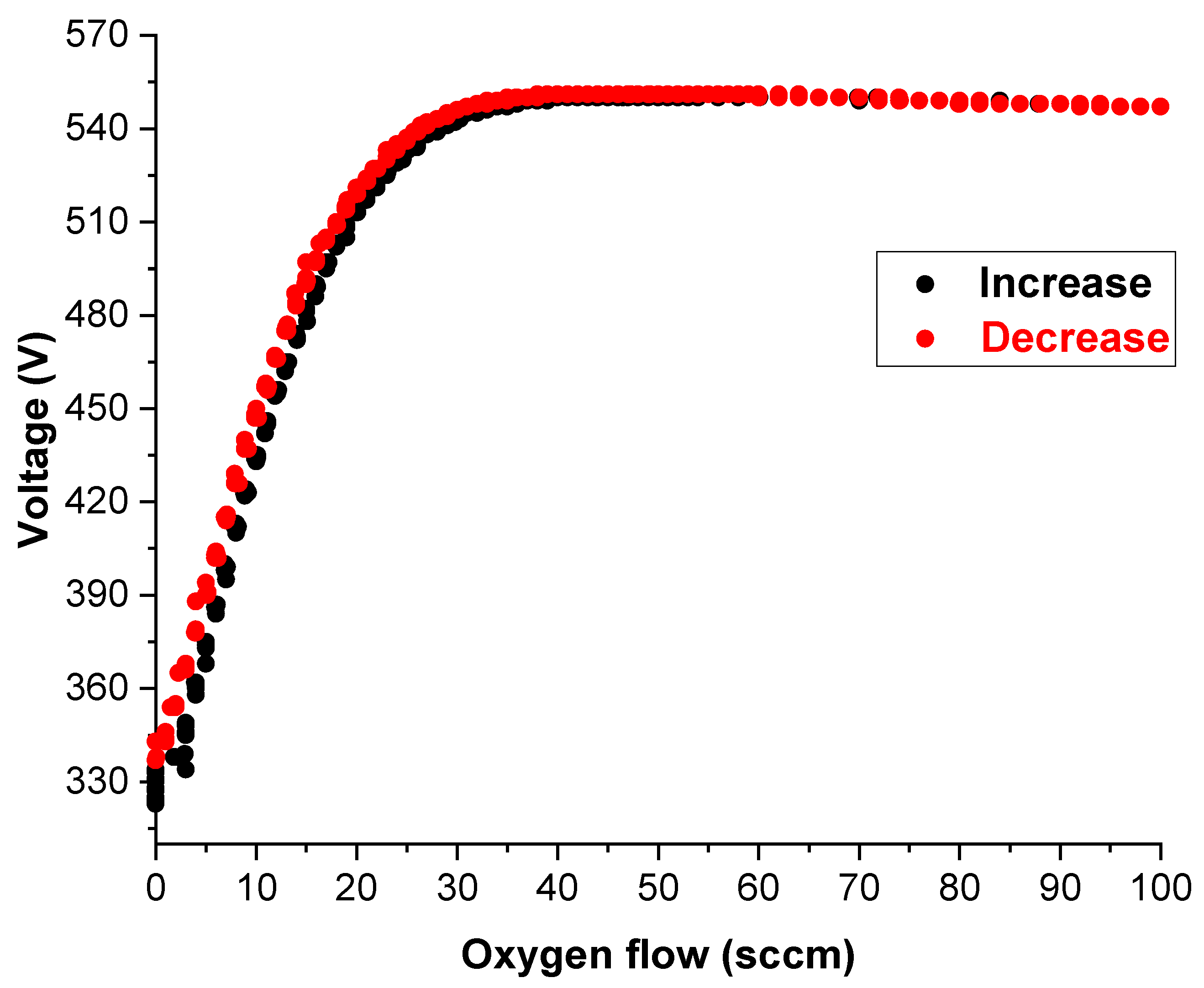
3.1. Alumina
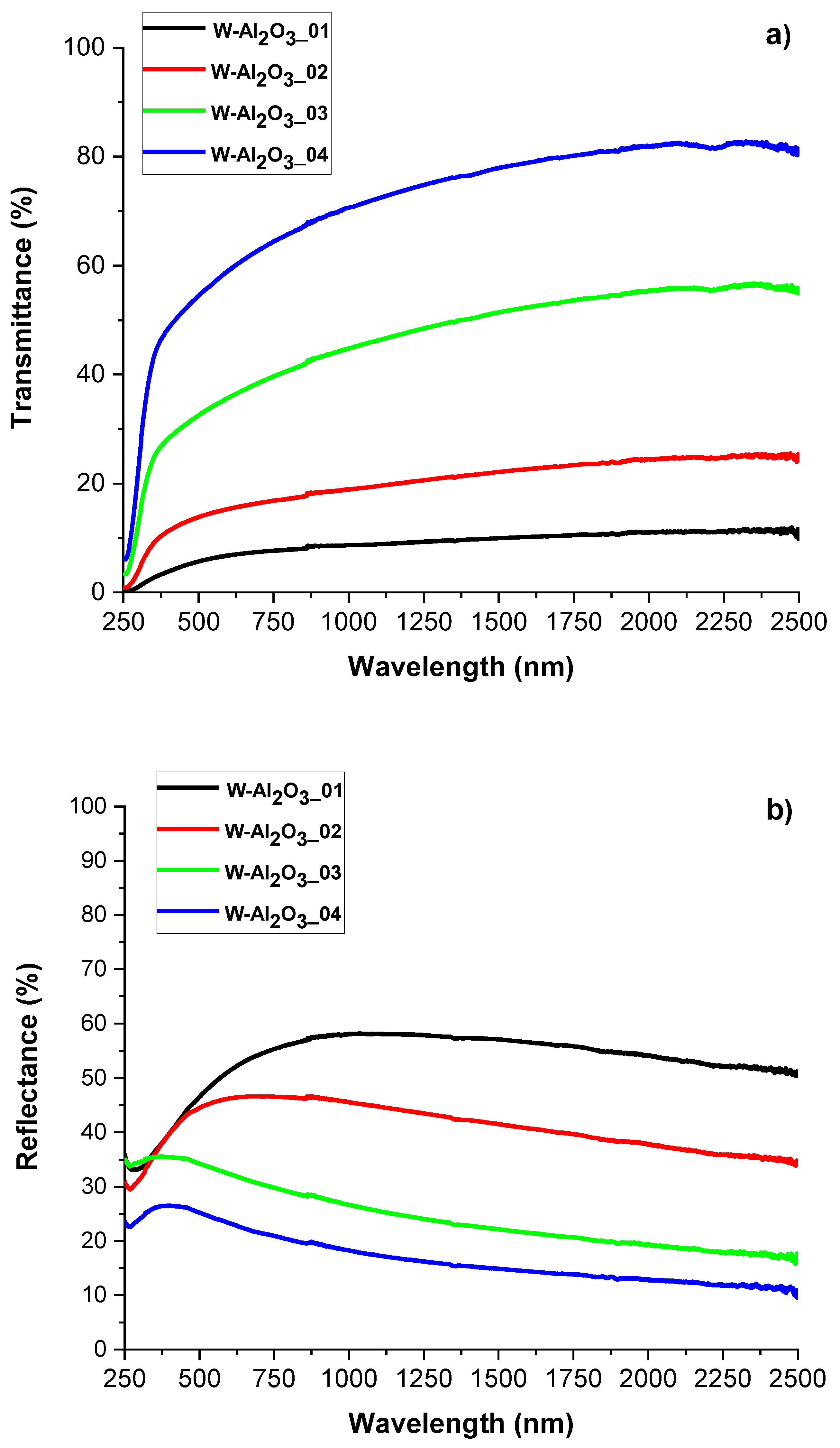
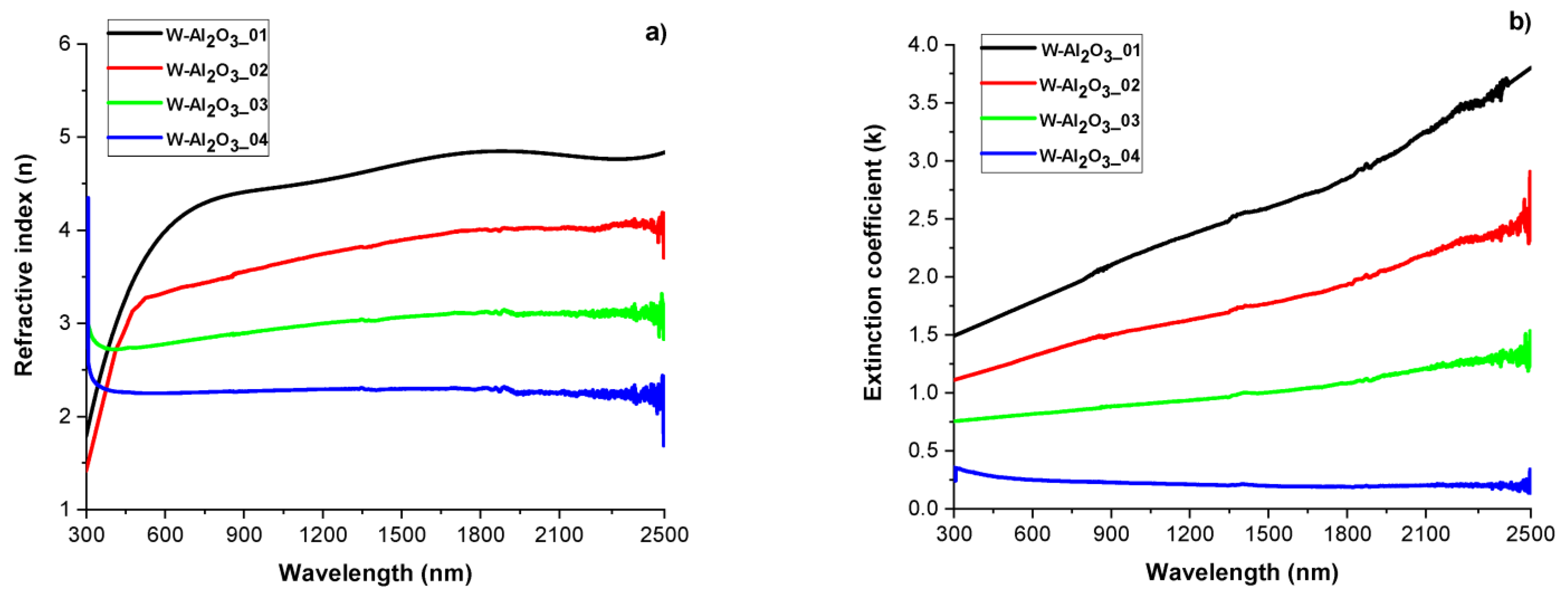
3.2. W-Al2O3 Cermet
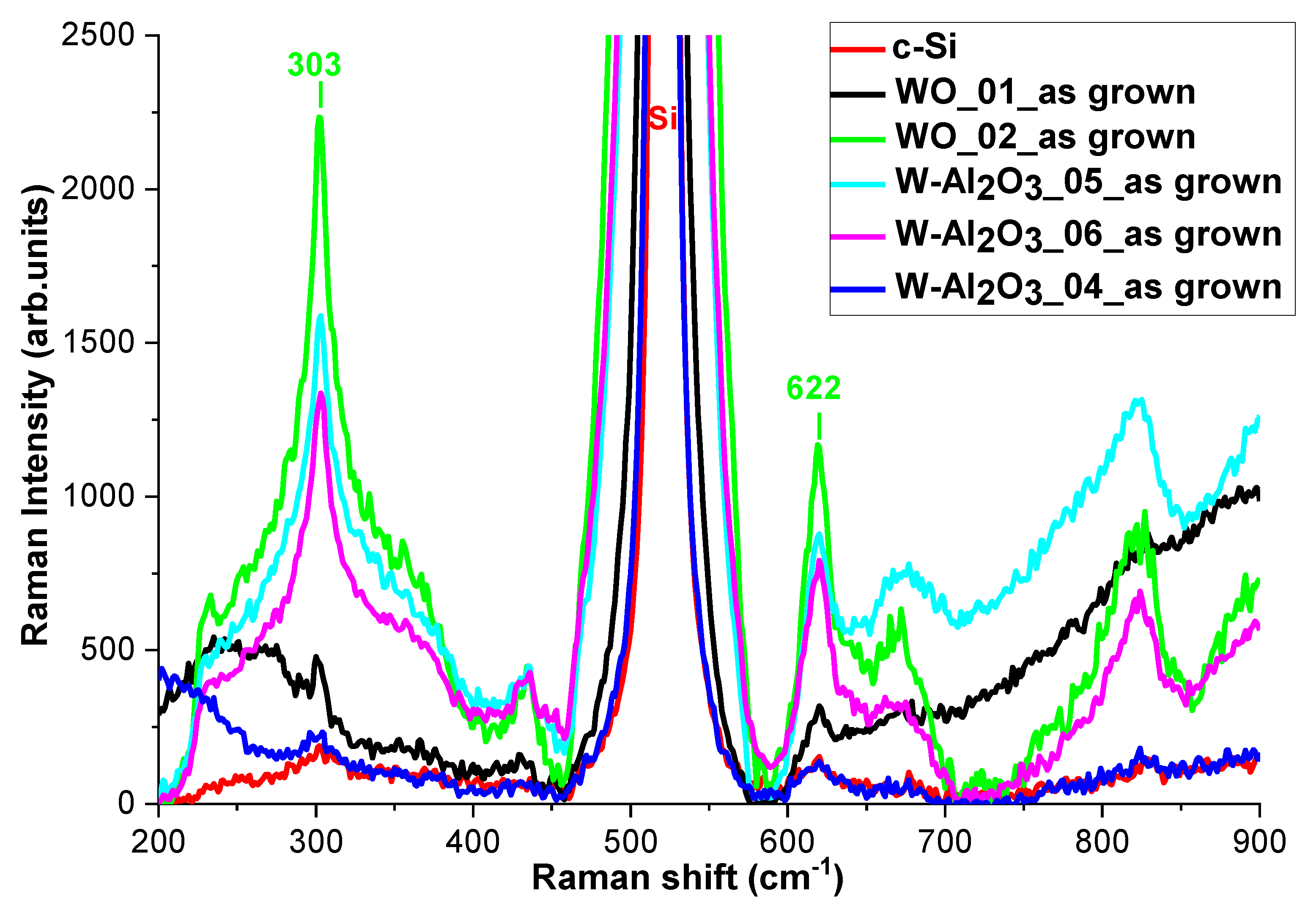
3.3. Structural Characterizations of the Realized Materials: XRD and Raman Measurements to W-O Bonds Detection
- During the deposition of the metallic component of cermet, the plasma contains residual reactive gas coming from the region where ceramic component growth is promoted. In this case, small quantities of tungsten oxide form because of the minimal presence of oxygen;
- During the exposition of the metallic component to the plasma containing the reactive gas that promotes the ceramic component growth (this exposure is due to the rotation of the tube holder), the formation of oxides is probably limited to the W cluster boundaries, which could play a passivating function, thus limiting a further oxidation of the internal regions of clusters. Furthermore, tungsten and aluminum are simultaneously present and the latter is characterized by a redox potential less positive than that of tungsten, thus, the formation of aluminum oxide is favored nevertheless [34].
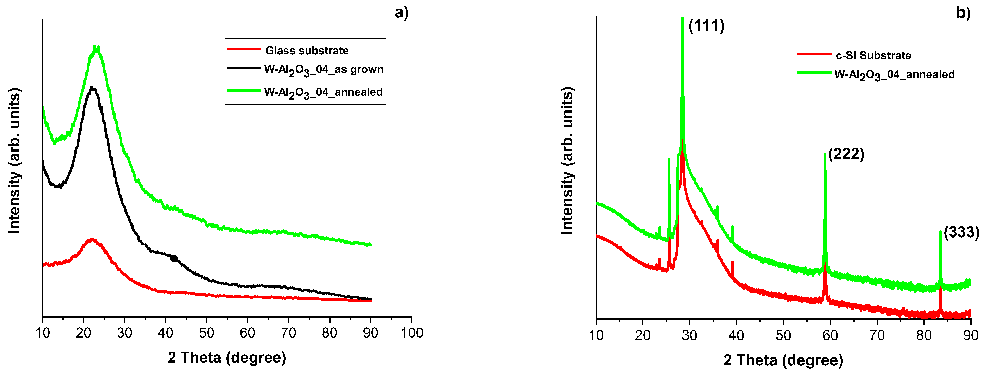
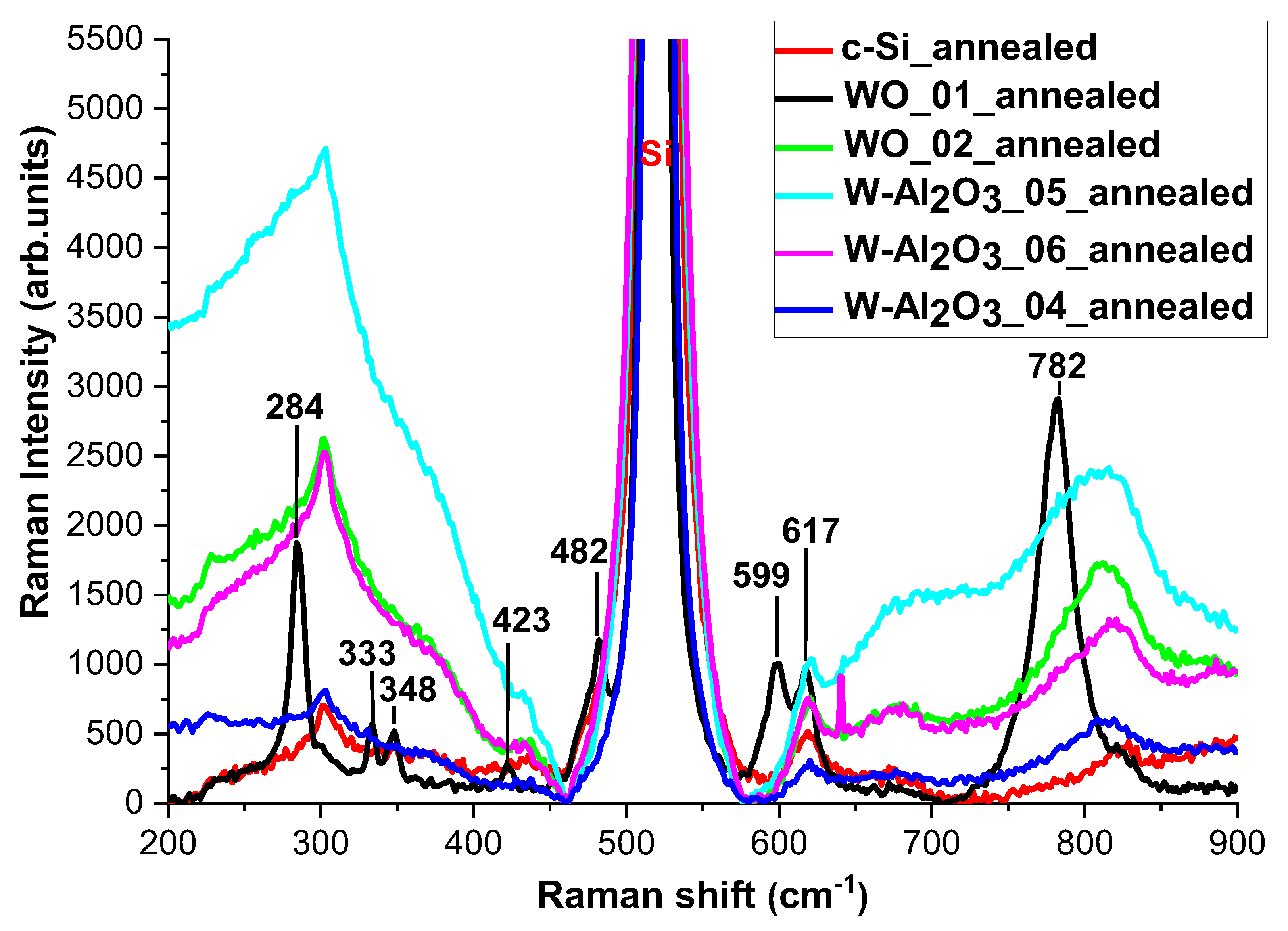
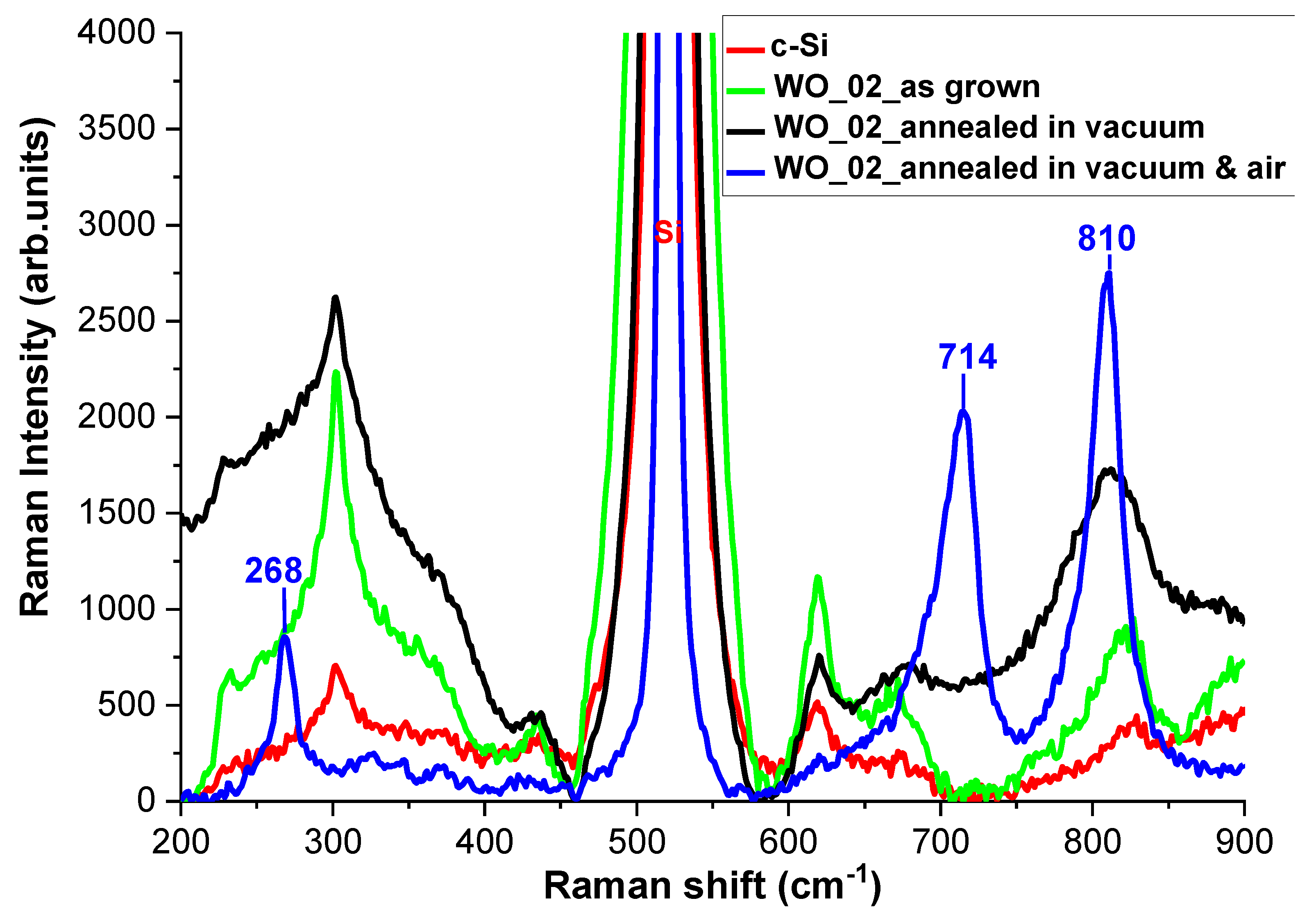
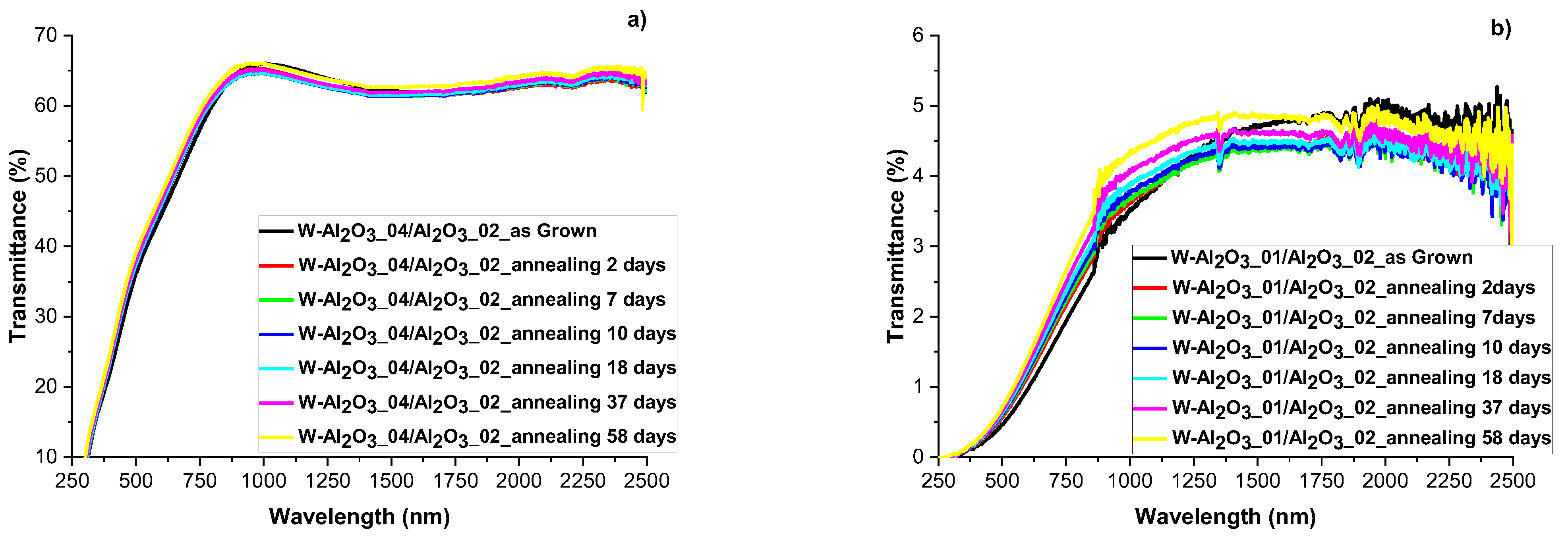
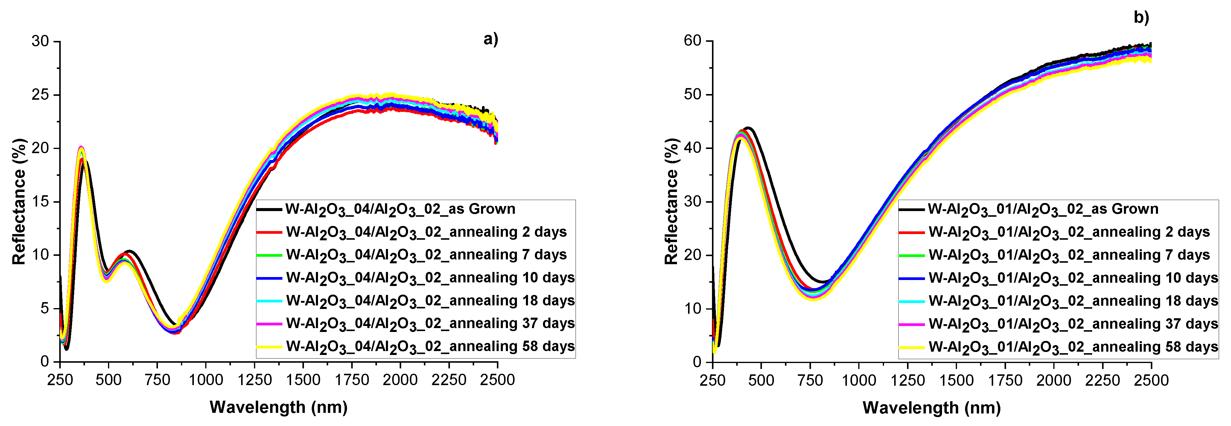
3.4. Evaluation of Optical and Structural Stability of Materials through Annealing Tests
4. Conclusions
Author Contributions
Funding
Institutional Review Board Statement
Informed Consent Statement
Data Availability Statement
Acknowledgments
Conflicts of Interest
References
- Selvakumar, N.; Barshilia, H.C. Review of physical vapor deposited (PVD) spectrally selective coatings for mid- and high-temperature solar thermal applications. Sol. Energy Mater. Sol. Cells 2012, 98, 1–23. [Google Scholar] [CrossRef]
- Bello, M.; Shanmugan, S. Achievements in mid and high-temperature selective absorber coatings by physical vapor deposition (PVD) for solar thermal Application—A review. J. Alloys Compd. 2020, 839, 155510. [Google Scholar] [CrossRef]
- Noc, L.; Jerman, I. Review of the spectrally selective (CSP) absorber coatings, suitable for use in SHIP. Sol. Energy Mater. Sol. Cells 2022, 238, 111625. [Google Scholar] [CrossRef]
- Ritchie, I.T.; Window, B. Applications of thin graded-index films to solar absorbers. Appl. Opt. 1977, 16, 1438–1443. [Google Scholar] [CrossRef]
- Sathiaraj, T.S.; Thangaraj, R.; Alsharbaty, H.; Bhatnagar, M.; Agnihotri, O.P. Ni-Al2O3 Selective Cermet Coatings for photothermal conversion up to 500 °C. Thin Solid Film. 1990, 190, 241–254. [Google Scholar] [CrossRef]
- Barshilia, H.C.; Kumar, P.K.; Rajam, S.; Biswas, A. Structure and optical properties of Ag–Al2O3 nanocermet solar selective coatings prepared using unbalanced magnetron sputtering. Sol. Energy Mater. Sol. Cells 2011, 95, 1707–1715. [Google Scholar] [CrossRef]
- Xinkang, D.; Cong, W.; Tianmin, W.; Long, Z.; Bulia, C. Microstructure and spectral selectivity of Mo-Al2O3 solar selective absorbing coatings after annealing. Thin Solid Films 2008, 516, 3971–3977. [Google Scholar] [CrossRef]
- Cheng, J.; Wang, C.; Wang, W.; Du, X.; Liu, Y.; Xue, Y. Improvement of thermal stability in the solar selective absorbing Mo–Al2O3 coating. Sol. Energy Mater. Sol. Cells 2013, 109, 204–208. [Google Scholar] [CrossRef]
- Tsegay, M.; Gebretinsae, H.; Sackey, J.; Arendse, C.; Nuru, Z. Structural and optical properties of Pt-Al2O3 double cermet as selective solar absorber. Mat. Today: Proc. 2021, 36, 571–575. [Google Scholar] [CrossRef]
- Chevapruk, T.; Chomcharoen, N.; Techapiesancharoenkij, R.; Kumnorkaew, P.; Muangnapoh, T.; Surawathanawises, K. Solution-based Ni-Al2O3 Solar Selective Coating using Convective Deposition. Mater. Today: Proc. 2020, 23, 745–751. [Google Scholar] [CrossRef]
- Antonaia, A.; Castaldo, A.; Addonizio, M.L.; Esposito, S. Stability of W-Al2O3 cermet based solar coating for receiver tube operating at high temperature. Sol. Energy Mater. Sol. Cells 2010, 94, 1604–1611. [Google Scholar] [CrossRef]
- Rebouta, L.; Sousa, A.; Capela, P.; Andritschky, M.; Santilli, P.; Matilainen, A.; Pischow, K.; Barradas, N.P.; Alves, E. Solar selective absorbers based on Al2O3:W cermets and AlSiN/AlSiON layers. Sol. Energy Mater. Sol. Cells 2015, 137, 93–100. [Google Scholar] [CrossRef]
- Zhou, J.; Li, S.; Yu, Y. First principle calculation of thermal conversion properties of W-Al2O3 based solar selective absorbing coating. Comput. Mater. Sci. 2022, 211, 111501. [Google Scholar] [CrossRef]
- Kathrein, M.; Schintlmeister, W.; Wallgram, W.; Schleinkofe, U. Doped CVD Al2O3 coatings for high performance cutting tools. Surf. Coat. Technol. 2003, 163–164, 181–188. [Google Scholar] [CrossRef]
- Mohammed, A.; Khodair, Z.T.; Khadom, A.A. Preparation, characterization and application of Al2O3 nanoparticles for the protection of boiler steel tubes from high temperature corrosion. Ceram. Int. 2020, 46, 26945–26955. [Google Scholar]
- Antonaia, A.; Esposito, S.; Addonizio, M.L.; Guglielmo, A. Solar Selective Absorber on Double Nitride Composite Material and Process for Its Preparation. Italy Patent IPNWO/2012/172505, 20 December 2012. [Google Scholar]
- MATS Project. Available online: http://www.mats.enea.it (accessed on 7 September 2021).
- Schiller, S.; Goedicke, K.; Reschke, J.; Kirchhoff, V.; Schneider, S.; Milde, F. Pulsed magnetron sputter technology. Surf. Coat. Technol. 1993, 61, 331–337. [Google Scholar] [CrossRef]
- Fietzke, F.; Goedicke, K.; Hempel, W. The deposition of hard crystalline Al2O3 layers by means of bipolar pulsed magnetron sputtering. Surf. Coat. Technol. 1996, 286–287, 657–663. [Google Scholar] [CrossRef]
- Musil, J.; Baroch, P.; Vlček, J.; Nam, K.; Han, J.G. Reactive magnetron sputtering of thin films: Present status and trends. Thin Solid Films 2005, 475, 208–218. [Google Scholar] [CrossRef]
- Madsen, N.; Christensen, B.H.; Louring, S.; Berthelsen, A.N.; Almtoft, K.P.; Nielsen, L.P.; Bøttiger, J. Controlling the deposition rate during target erosion in reactive pulsed DC magnetron sputter deposition of alumina. Surf. Coat. Technol. 2012, 206, 4850–4854. [Google Scholar] [CrossRef]
- Carreri, F.C.; Bandorf, R.; Gerdes, H.; Vergöhl, M.; Bräuer, G. Highly insulating alumina films by a bipolar reactive MF sputtering process with special arc handling. Surf. Coat. Technol. 2016, 290, 82–86. [Google Scholar] [CrossRef]
- Wallin, E.; Helmersson, U. Hysteresis-free reactive high power impulse magnetron sputtering. Thin Solid Films 2008, 516, 6398–6401. [Google Scholar] [CrossRef] [Green Version]
- Safi, I. Recent aspects concerning DC reactive magnetron sputtering of thin films: A review. Surf. Coat. Technol. 2000, 27, 203–218. [Google Scholar] [CrossRef]
- Becerril-Gonzalez, J.J.; Castro-Chong, A.M.; Oskam, G.; Arés-Muz, O. Sputter deposition of Mo-alumina cermet solar selective coatings: Interrelation between residual oxygen incorporation, structure and optical properties. Mater. Res. Express 2021, 8, 105506. [Google Scholar] [CrossRef]
- Esposito, S.; D'Angelo, A.; Diletto, C.; Guglielmo, A.; Lanchi, M.; Rossi, G. Solar Coatings Based on Ag Infrared Reflector with High Stability at Medium and High Temperature. Energies 2021, 14, 5910. [Google Scholar] [CrossRef]
- D'Angelo, A.; Diletto, C.; Esposito, S.; Graditi, G.; Guglielmo, A.; Lanchi, M.; Rossi, G. Spectrally selective solar coating based on W-AlN cermet fabricated by reactive sputtering processes at high deposition rate. AIP Conf. Proc. 2022, 2445, 020002. [Google Scholar]
- Takenaka, K.; Setsuhara, Y.J.; Han, G.; Uchida, G.; Ebe, A. High-rate deposition of silicon nitride thin films using plasma-assisted reactive sputter deposition. Thin Solid Films 2019, 685, 306–311. [Google Scholar] [CrossRef]
- Cheng, Y.H.; Lee, P.I.; Sakalley, S.; Wen, C.K.; Cheng, W.C.; Sun, H.; Chen, S.C. Enhanced Electrical Properties of Copper Nitride Films Deposited via High Power Impulse Magnetron Sputtering. Nanomaterials 2022, 12, 2814. [Google Scholar] [CrossRef]
- Nadel, S.J.; Greene, P.; Rietzel, J.; Strümpfel, J. Equipment, materials and processes: A review of high rate sputtering technology for glass coating. Thin Solid Films 2003, 442, 11–14. [Google Scholar] [CrossRef]
- Blackburn, P.E.; Hoch, M.; Johnston, H. The vaporization of Molybdenum and Tungsten Oxides. J. Phys. Chem. 1958, 62, 769–773. [Google Scholar] [CrossRef]
- Gulbransen, E.A.; Andrew, K.F. Kinetics of the Oxidation of Pure Tungsten from 500 °C to 1300 °C. J. Electrochem. Soc. 1960, 107, 619–628. [Google Scholar] [CrossRef]
- De Sio, A.; Madena, T.; Huber, R.; Parisi, J.; Neyshtadt, S.; Deshler, F.; Da Como, E.; Esposito, S.; Von Hauff, E. Solvent additives for tuning the photovoltaic properties of polymer–fullerene solar cells. Sol. Energy Mater. Sol. Cells 2011, 95, 3536–3542. [Google Scholar] [CrossRef]
- Kuckelkorn, T.; Graf, W.; Hildebrandt, C.; Georg, A. Radiation Selective Absorber Coating for an Absorber Pipe, Absorber Pipe with Said Coating, and Method of Making Same. US Patent US7,909,029 B2, 27 November 2006. [Google Scholar]
- Romanyuk, A.; Oelhafen, P. Evidence of different oxygen states during thermal coloration of tungsten oxide. Sol. Energy Mater. Sol. Cells 2006, 90, 1945–1950. [Google Scholar] [CrossRef]
- Maffeis, T.G.; Yung, D.; LePennec, L.; Penny, M.W.; Cobley, R.J.; Comini, E.; Sberveglieri, G.; Wilks, S.P. STM and XPS characterisation of vacuum annealed nanocrystalline WO3 films. Surf. Sci. 2007, 601, 4953–4957. [Google Scholar] [CrossRef]
- Maffeis, T.G.; Penny, M.W.; Cobley, R.J.; Comini, E.; Sberveglieri, G.; Wilks, S.P. XPS Characterisation of vacuum annealed nanocrystalline WO3 films. e-J. Surf. Sci. Nanotechnol. 2009, 7, 319–322. [Google Scholar] [CrossRef]
- Shapovalov, V.I.; Lapshin, A.E.; Gagarin, A.G.; Efimenko, L.P. Chemical composition and crystal structure of tungsten oxide films. Glass Phys. Chem. 2014, 40, 553–569. [Google Scholar] [CrossRef]
- Chou, T.C.; Adamson, D.; Mardinly, J.; Nieh, T.G. Microstructural evolution and properties of nanocrystalline alumina made by reactive sputtering deposition. Thin Solid Film. 1991, 205, 131–139. [Google Scholar] [CrossRef]
- Musil, J.; Blažek, J.; Zeman, P.; Prokšová, Š.; Šašek, M.; Čerstvý, R. Thermal stability of alumina thin films containing γ-Al2O3 phase prepared by reactive magnetron sputtering. Appl. Surf. Sci. 2010, 257, 1058–1062. [Google Scholar] [CrossRef]
- Edlmayr, V.; Moser, M.; Walter, C.; Mitterer, C. Thermal stability of sputtered Al2O3 coatings. Surf. Coat. Technol. 2010, 204, 1576–1581. [Google Scholar] [CrossRef]
- Parreira, N.M.; Carvalho, N.J.; Cavaleiro, A. Synthesis, structural and mechanical characterization of sputtered tungsten oxide coatings. Thin Solid Films 2006, 510, 191–196. [Google Scholar] [CrossRef]
- Manciu, F.S.; Enriquez, J.L.; Durrer, W.G.; Yun, Y. Spectroscopic analysis of tungsten oxide thin films. J. Mater. Res. 2010, 25, 2401–2406. [Google Scholar] [CrossRef]
- Besozzi, E.; Dellasega, D.; Russo, V.; Conti, C.; Passoni, M.; Beghi, M.G. Thermomechanical properties of amorphous metallic tungsten-oxygen and tungsten-oxide coatings. Mater. Des. 2019, 165, 107565. [Google Scholar] [CrossRef]
- Frey, G.L.; Rothschild, A.; Sloan, J.; Rosentsveig, R.; Popovitz-Biro, R.; Tenne, R. Investigations of Nonstoichiometric Tungsten Oxide Nanoparticles. J. Solid State Chem. 2001, 162, 300–314. [Google Scholar] [CrossRef]
- Kumar, V.B.; Mohanta, D. Formation of nanoscale tungsten oxide structures and colouration characteristics. Bull. Mater. Sci. 2011, 34, 435–442. [Google Scholar]
- Daniel, M.F.; Desbat, B.; Lassegue, J. Infrared and Raman Study of WO3 Tungsten Trioxide and WO3xH2O Tungsten Trioxide Hydrates. J. Solid State Chem. 1987, 67, 235–247. [Google Scholar] [CrossRef]


| Process Parameters | Al2O3_01 | Al2O3_02 | Al2O3_03 |
|---|---|---|---|
| Argon flow (sccm) | 400 | 400 | 400 |
| Oxygen flow (sccm) | 5 | 5.4 | 5.6 |
| Process pressure (Pa) | ~1 | ~1 | ~1 |
| Al power density (W/cm2) | 1.84 | 1.84 | 1.84 |
| Intensity of emission spectral line of Al (Cts) | 40,000 | 38,000 | 36,000 |
| Deposition rate (Å/s) | 0.79 | 0.71 | 0.66 |
| Process Parameters | W-Al2O3_01 | W-Al2O3_02 | W-Al2O3_03 | W-Al2O3_04 |
|---|---|---|---|---|
| Argon flow (sccm) | 400 | 400 | 400 | 400 |
| Oxygen flow (sccm) | 5.8 | 5.6 | 5.5 | 5.4 |
| Process pressure (Pa) | ~1 | ~1 | ~1 | ~1 |
| Al power density (W/cm2) | 1.84 | 1.84 | 1.84 | 1.84 |
| W power density (W/cm2) | 9.78 | 6.67 | 3.56 | 1.33 |
| Intensity of emission spectral line of Al (Cts) | 30,000 | 35,000 | 35,000 | 35,000 |
| Thickness (Å/s) | 508 | 421 | 299 | 395 |
| Process Parameters | W-Al2O3_04 | W-Al2O3_05 | W-Al2O3_06 | WO_01 | WO_02 |
|---|---|---|---|---|---|
| Argon flow (sccm) | 400 | 400 | 400 | 400 | 400 |
| Oxygen flow (sccm) | 5.4 (PEM) | 19 (Al side) | 19 (Al side) + 35 (W side) | 12 (W side) | 40 (W side) |
| Process pressure (Pa) | ~1 | ~1 | ~1 | ~1 | ~1 |
| Al power density (W/cm2) | 1.84 | 1.84 | 1.84 | / | / |
| W power density (W/cm2) | 1.33 | 1.33 | 1.33 | 1.33 | 1.33 |
Disclaimer/Publisher’s Note: The statements, opinions and data contained in all publications are solely those of the individual author(s) and contributor(s) and not of MDPI and/or the editor(s). MDPI and/or the editor(s) disclaim responsibility for any injury to people or property resulting from any ideas, methods, instructions or products referred to in the content. |
© 2023 by the authors. Licensee MDPI, Basel, Switzerland. This article is an open access article distributed under the terms and conditions of the Creative Commons Attribution (CC BY) license (https://creativecommons.org/licenses/by/4.0/).
Share and Cite
Diletto, C.; D’Angelo, A.; Esposito, S.; Guglielmo, A.; Mirabile Gattia, D.; Lanchi, M. Materials Based on Amorphous Al2O3 and Composite W-Al2O3 for Solar Coatings Deposited by High-Rate Sputter Processes. Solar 2023, 3, 113-131. https://doi.org/10.3390/solar3010009
Diletto C, D’Angelo A, Esposito S, Guglielmo A, Mirabile Gattia D, Lanchi M. Materials Based on Amorphous Al2O3 and Composite W-Al2O3 for Solar Coatings Deposited by High-Rate Sputter Processes. Solar. 2023; 3(1):113-131. https://doi.org/10.3390/solar3010009
Chicago/Turabian StyleDiletto, Claudia, Antonio D’Angelo, Salvatore Esposito, Antonio Guglielmo, Daniele Mirabile Gattia, and Michela Lanchi. 2023. "Materials Based on Amorphous Al2O3 and Composite W-Al2O3 for Solar Coatings Deposited by High-Rate Sputter Processes" Solar 3, no. 1: 113-131. https://doi.org/10.3390/solar3010009