Article

Advanced Technologies in the Fabrication of a Micro-Optical Light Splitter

by
Giovanna Stella
1,*,
Lorena Saitta
2,
Alfredo Edoardo Ongaro
3,
Gianluca Cicala
2,
Maïwenn Kersaudy-Kerhoas
3 and
Maide Bucolo
1,*
1
Department of Electrical, Electronic and Computer Engineering, University of Catania, Viale A. Doria 6, 95125 Catania, Italy
2
Department of Civil Engineering and Architecture, University of Catania, Viale A. Doria 6, 95125 Catania, Italy
3
School of Engineering and Physical Sciences, Heriot-Watt University, Edinburgh EH14 4AS, UK
*
Authors to whom correspondence should be addressed.
Micro 2023, 3(1), 338-352; https://doi.org/10.3390/micro3010023
Submission received: 21 January 2023 / Revised: 19 February 2023 / Accepted: 3 March 2023 / Published: 10 March 2023

Abstract

:
In microfluidics, it is important to confine and transport light as close as possible to the sample by guiding it into a small volume of the microfluidic channel, acquiring the emitted/transmitted radiation. A challenge in this context is the miniaturization of the optical components and their integration into the microfluidic device. Among all of the optical components, a particular role is played by the beam splitter, an important optical device capable of splitting light into several paths. In this paper, a micro-splitter is designed and realized by exploiting low-cost technologies. The micro-splitter consists of a micro-mirror in-between two micro-waveguides. This component was fabricated in different materials: poly-dimethyl-siloxane (PDMS), poly(methyl methacrylate) (PMMA), and VeroClear RGD810. A 3D printing master–slave fabrication protocol was used with PDMS, a direct 3D printing approach with VeroClear, and a laser cutting procedure with PMMA. The experimental results obtained show the high potential of the proposed fabrication protocols, based on low-cost technologies, for the realization of micro-optical components, which could also be easily integrated with microfluidics systems.

1. Introduction

In microfluidics, it is important to confine and transport the light as close as possible to the sample by guiding it into a small volume of the microfluidic channel and acquiring the emitted/transmitted radiation. Several optical components were realized to fulfill this purpose. Moreover, current research is dedicated to the fabrication of micro-optical components; researchers are investigating different manufacturing technologies and analyzing their integration with microfluidic devices, such as micro-waveguide [1,2,3,4], micro-mirror [5], and micro-lens [6,7,8]. The fabrication of optical components integrated with microfluidic channels is not a simple process. It is mainly based on photolithography, a complex procedure dependent on the substrate of choice, e.g., silica on silicon [9,10], ion exchange [11], or polymers [12].
Focusing on the polymer, according to the state-of-the-art and the research studies recently performed, different materials have been identified as suitable for fabricating low-loss optical components. Among these, the main candidates are poly(methyl methacrylate) (PMMA), polyamides, siloxanes, and polycarbonates. Indeed, their use is widespread in this field, since the commercial availability of plastic optical components makes it one of the most cost-effective and consistent optical components in production today [13].
The first fabrication of a POF (plastic optical fiber), by exploiting the 3D printing approach, dates back to 2015 [14]. Since that moment, many different materials have been used for this purpose, such as acrylonitrile butadiene styrene (ABS) and polyethylene terephthalate glycol (PETG). Their uses were justified by the fact that they were commoditized and easily accessible. However, as a drawback, they were characterized by poor optical properties and very high losses. For this reason, later, their uses were replaced by resins, classified as optical grade polymers, since they have lower optical losses. Common resins that fall into this class of materials are cyclic olefin polymers (COP), poly(methyl methacrylate) (PMMA), polycarbonate (PC), and poly(styrene) (PS). According to the state-of-the-art, all of them are commonly used to 3D print polymer optical components [15]. Furthermore, the use of the aforementioned polymer materials allows one to approach the performance of the gold standard material for optical components, i.e., glass.
Nowadays, microfabrication techniques, which are capable of easily integrating optical waveguides into a lab-on-a-chip (LOC), are in high demand. Among these, 3D printing has been identified as a progressive and effective manufacturing technology by offering the possibility to rapidly and economically realize complex 3D structures with different materials [16,17]. High-quality 3D printing microfluidics devices have been realized [18,19,20,21].
Among all of the optical components, one particular role is played by the beam splitter. It is an important optical device whose optical power splitting ratio at the respective output ports can be dynamically manipulated. In recent decades, micro-splitters were presented with different geometries [22,23,24] and costly techniques [25,26,27]. In this paper, a micro-splitter was designed and realized by exploiting low-cost technologies. This component was fabricated into different materials, i.e., poly-dimethyl-siloxane (PDMS), poly(methyl methacrylate) (PMMA), and VeroClear RGD810. A 3D printing master–slave fabrication protocol was used with PDMS, a direct 3D printing approach with the VeroClear, and a laser cutting procedure with PMMA. In line with the literature, both the PDMS and the PMMA are suitable polymers for the purpose of this paper, i.e., the fabrication of polymer optical components. For this reason, they were selected and their uses were combined with proper manufacturing techniques, which are the 3D print master–slave fabrication protocol and laser cutting, respectively, to realize a low-cost micro-optical splitter. Additionally, as the VeroClear RGD810 is a transparent PolyJetTM photopolymer that simulates the PMMA (according to the Stratasys technical data sheet for the material), it was selected as a suitable material to realize micro-optical components by a direct inkjet 3D printing fabrication. Some examples of micro-optofluidic systems based on specific realization protocols were presented in [28,29]. This shows the potential of this technology for LOC applications. Furthermore, another cost-effective prototyping technique is laser-based microengineering [30,31,32]. It is fast and can elegantly address the need for rapid design cycles [33].
In [34], the two low-cost technologies mentioned, i.e., 3D printing PDMS-based and laser-cutting PMMA-based, were investigated as novel methods to realize micro-optical waveguides. The results obtained have shown the possibility of using low-cost technologies for the realization of micro-optical waveguides suitable for integration in micro-optofluidic devices and the potential for creating micro-optical paths inside microsystems. In this paper, the micro-splitter design, the ray-tracing simulations, and the three chosen manufacturing processes are presented in Section 2. The experimental characterization of the fabricated micro-optical components and a comparative analysis between them are discussed in Section 3. The obtained experimental results prove the high potential of the proposed fabrication protocols, based on low-cost technologies, for the realization of micro-optical components, which are easily integrable with microfluidic systems [29].

2. Materials and Methods

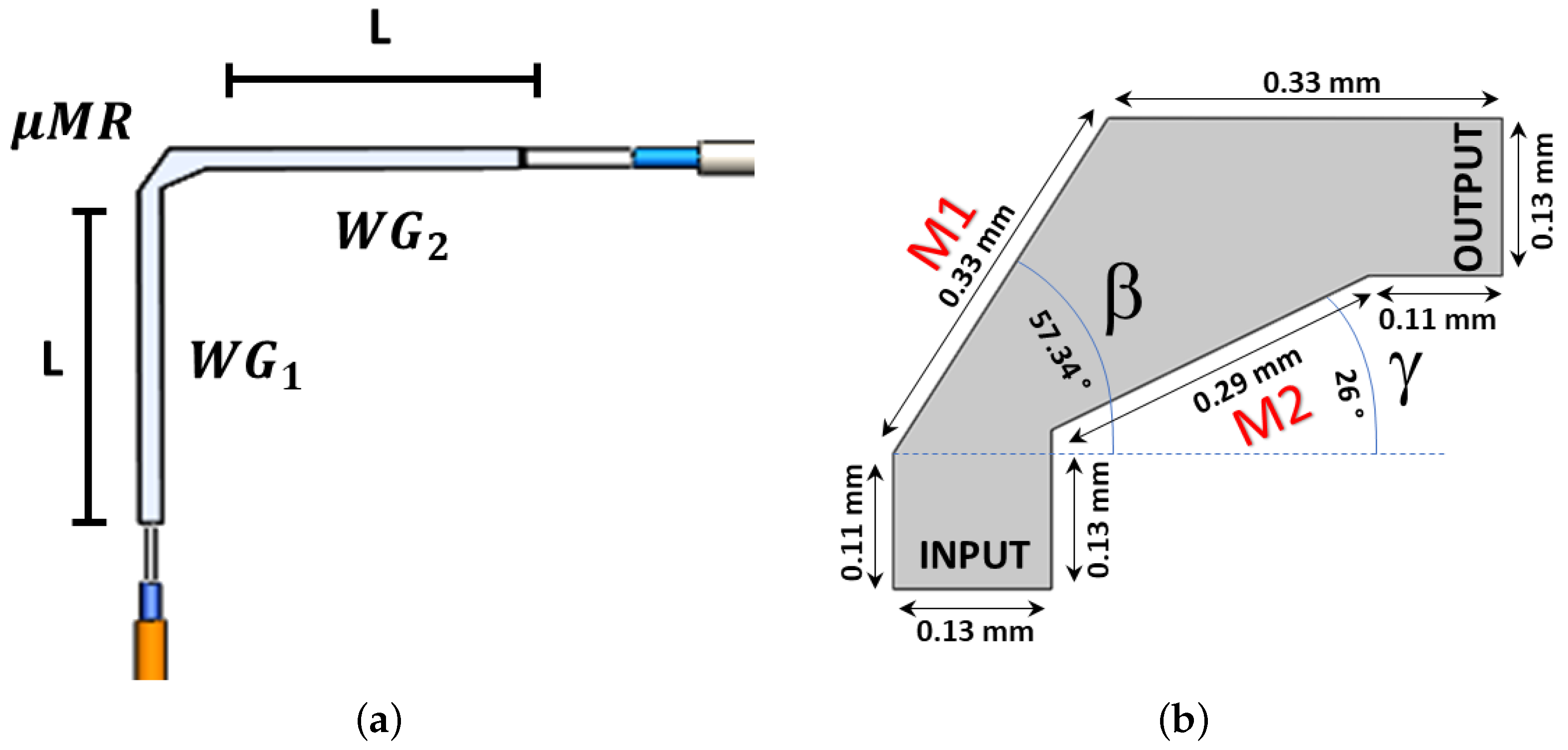
2.1. Design and Simulations

The micro-optical component presented in this paper, i.e., the micro-splitter ( μ S P T ), was realized by including a micro-mirror ( μ M R ) in-between two micro-waveguides ( μ W G s ) of length L as shown in Figure 1a. It bends the light beam from the input source; the working principle is as follows: an input optical fiber guides the light, coming from the laser, through the first waveguide ( μ W G 1 ) toward the micro-mirror ( μ M R ). The light, after being angled by the latter, is guided to the output optical fiber by the second waveguide ( μ W G 2 ). The μ M R geometry consists of two angled surfaces, M 1 and M 2 , respectively, tilted at the angles { β , γ } , with respect to the light input section, as shown in Figure 1b. The optimal values of { β , γ } were identified by ray-tracing simulations (TracePro, Lambda Research Corporation, Westford, MA, USA) as shown in Figure 2.
Initially, only one surface M 1 was considered with an inclination β = 45 to bend the rays coming from the input (see Figure 2a). Due to the laser N A = 0.22 , the light travels inside the device with an initial angle of θ = s i n ( N A ) = 11 and it is bent at the wall. The μ M R was assumed to be surrounded by air with a refractive index n 0 = 1 , and the three materials selected to realize the micro-optical components have different refractive indices: PDMS ( n 1 = 1.34 ), the PMMA ( n 1 = 1.41 ), and the VeroClear ( n 3 = 1.53 ). For the light transmission inside the micro-mirror, it is important to have total internal reflection. Based on Snell’s law (i.e., to have the total internal reflection), the angle between the rays and perpendicular to the surface M 1 should have been greater than a critical value, which depends on the material: φ c r i t P D M S = 48 , φ c r i t P M M A = 45 , φ c r i t V e r o C l e a r = 41 . Three points P i , with i = 1 , 2 , 3 on the surface M 1 were considered to trace the light path of the incident rays using the incident ( φ i ), transmitting ( ϵ i ), and reflected ( α i ) angles. In Figure 2a, for the PDMS- μ M R , the incident angles at the three points are reported: P 1 ( φ 1 = 34 ), P 2 ( φ 2 = 40 ), and P 3 ( φ 3 = 60 ). It is evident that only P 3 respected the condition for the total internal reflection. Then, angle β was increased and the optimal performance was obtained with β = 57 . 35 . Additionally, to contain all of the rays inside the optical path, a second reflection surface M 2 , with an inclination of φ = 26 , was designed (see Figure 2b). This design led to the minimization of the ray dispersion and conveyed the beam along the micro-optical device path toward the output light section. In Figure 2c, the complete path of the rays inside the PDMS- μ M R is shown; the laser source was assumed to have a power of 10 mW and able to emit 100 rays. Bumping on the wall ( M 1 ) was always reflected. The rays closer to point P 1 directly reached the output section; the rays closer to point P 3 were bent again at points P 4 and P 5 before reaching the output section (having the total internal reflection in both cases). These two light paths allowed the light to be split in two directions at the output section.
The micro-splitter ( μ S P T ) was designed with a squared section of 1 mm side; the input and output of the μ M R were lengthened, in continuity, on both sides by a length L (see Figure 1a). For L = 0 cm, the μ S P T design match with the μ M R . By setting L = 2 cm, the total length of the μ S P T was 4 cm.
The μ S P T performance was studied by ray-tracing simulations, assuming a laser source with a power of 10 mW that was able to emit 100 rays. The diameters of the input and output optical fibers were set, respectively, to 400 μ m and 1 mm, while the distance between them and the μ S P T was ideally set to zero. The results obtained by the ray-tracing simulations are reported in the histogram of Figure 3, where the percentage of rays reaching the output optical fiber surfaces for two different lengths L = {0; 2} cm are compared to the PMMA- μ S P T , the PDMS- μ S P T , and the VeroClear- μ S P T . In all of the cases, 60 % of the rays reached the output fiber surface, with an increase of 8 % for L = 0 cm, and the performances of the three materials were almost equivalent with a variation between 2 % and 8 % . At the μ S P T output section, the two light paths, obtained after the rays were bent by the μ M R (see Figure 2c), become more evident (see Figure 4). By analyzing the principal directions of the two light beams, an angle of about 36 , with respect to the output section of the μ M R , was identified (see Figure 4). Then, this design was characterized to guide and split the light rays in these two directions.

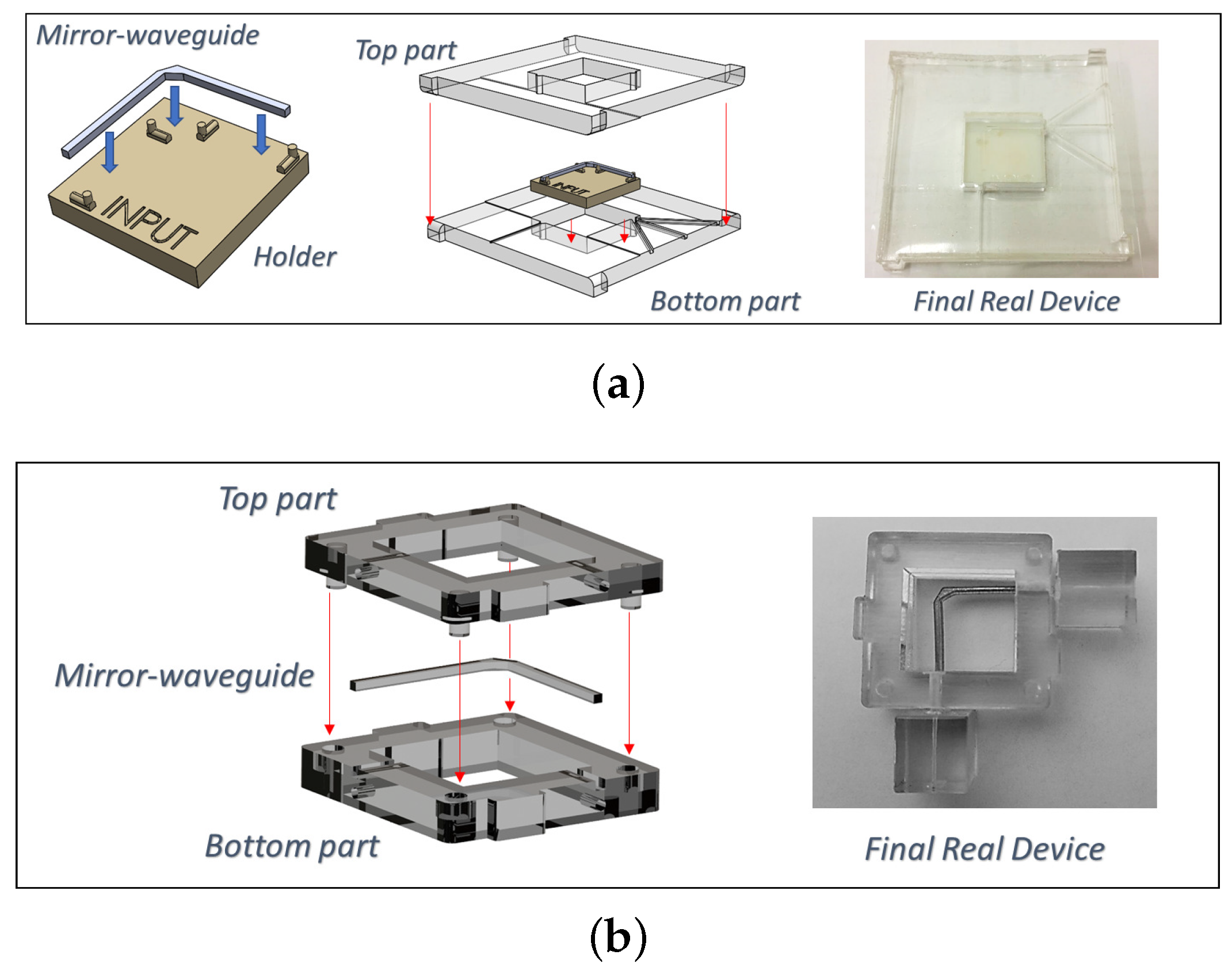
2.2. Fabrication Processes

For the fabrication of the μ S P T , based on the materials investigated, three low-cost technologies were taken into account. The realization of the PDMS- μ S P T was conducted using a master–slave approach based on the 3D printing technique implemented by the authors and previously presented in [28,29,34]. The PMMA- μ S P T was realized using a laser cutting fabrication technique. It was designed and laser-cut in 2 mm and 1 mm thick sheets (Cast ClarexTM Acrylic, Easter Road Plastics, Edinburgh, UK) using a laser-cutting instrument (Epilog Mini 18 30 W, EpilogLaser, Golden, CO, USA). The procedure adopted for the realization is similar to the others. The top and the bottom were cut in 2 mm sheets and the suspended PMMA- μ S P T was cut in a 0.2 mm layer with a distance (d) of 240 μ m. Then, the layers were bonded using two-minute thermal and solvent-assisted bonding. The details of the process are reported in [33,34]. VeroClear- μ S P T was directly 3D printed by using an inkjet 3D printer model (Objet260 Connex1, Stratasys, Los Angeles, CA, USA). The latter 3D printer was also used for the manufacturing of the master–slave mold exploited for the PDMS- μ S P T fabrication. The formulations of the used commercial resins, named VeroClear RGD810 (used for the VeroClear- μ S P T ) and Vero PureWhite RGD837 (used for the master–slave mold), were developed for the PolyJet 3D printing technique by Stratasys and they are proprietary. However, according to the safety data sheet (SDS), they are made of a complex mixture of photoactivation and acrylate monomers. Once the building procedure was accomplished, the support material was removed and, in the end, the 3D printed parts were soaked in a 1% solution of sodium hydroxide to obtain a smoother surface, as suggested by the Stratasys post-printing process guide.

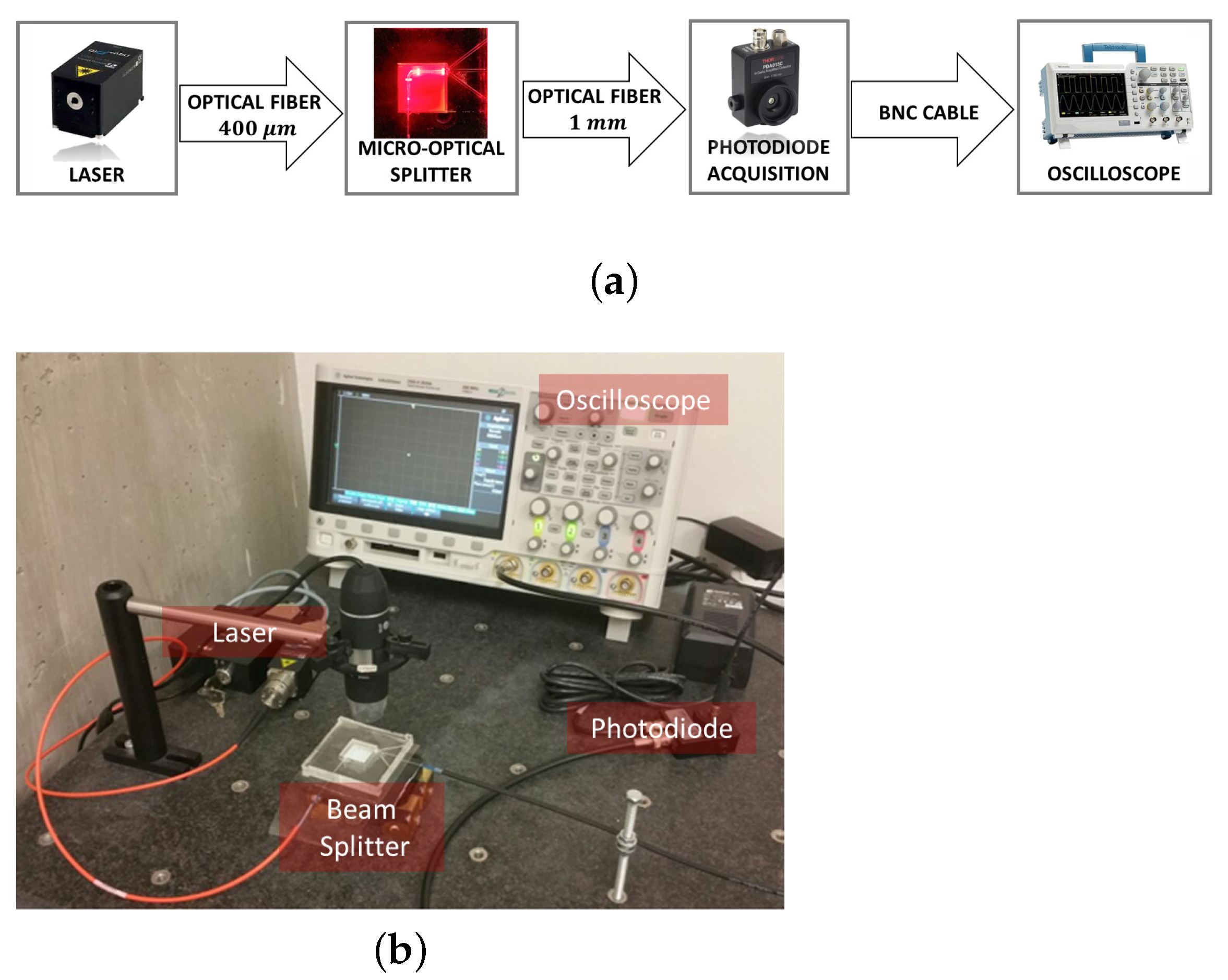
2.3. Experimental Set-Up

For the characterization of this micro-component, the PDMS- μ S P T , a support structure (as a testing platform) was realized in a way that it was surrounded by air. It was 3D printed with 4 pegs designed to touch the PDMS- μ S P T as little as possible to minimize the ray dispersion (see Figure 5a). For the alignment of the input and output fibers with the PDMS- μ S P T , two PDMS frames were used to surround the holder with two slots for the fibers insertions; the same approach was previously used in [34]. The center of Figure 5a shows the mounting scheme, while a picture of the complete micro-optical characterization system is shown on the right. The same design was considered for the realization of the support structure used for the characterization of VeroClear- μ S P T . VeroClear- μ S P T and its support system were directly 3D printed by using the inkjet 3D printer (Objet260 Connex1, Stratasys, Los Angeles, CA, USA); the steps in the realization of the testing platform are shown in Figure 5b. In particular, both the top and bottom cover parts designed for the μ S P T insertion together with the optical fiber supports, which ensured their aligned insertion, are reported on the left and the complete test platform on the right.
Regarding the PMMA- μ S P T , both the μ S P T and its support system were realized by using the laser cutting fabrication by combining three layers of sheets with the μ S P T in the middle, as reported in [34]. The flow chart and the picture of the experimental set-up, used for the μ S P T characterization, are shown in Figure 6a,b. The input light source was a laser system (NovaPro 660-125, RGB Lasersystems, Kelheim, Germany); this generated a light beam with a wavelength of 660 nm and a maximum output power of 125 mW. The output acquisition system consisted of a photo-diode (PDA100A, Thorlabs, Newton, NJ, USA) connected with a digital oscilloscope (SDS1102X, Siglent, Augsburg, Germany). The input and output of the μ S P T s were coupled with multi-mode optical fibers with core diameters, respectively, of { 365 ± 14 , 910 ± 30 } μm and N A = 0.22 .

3. Results and Discussion
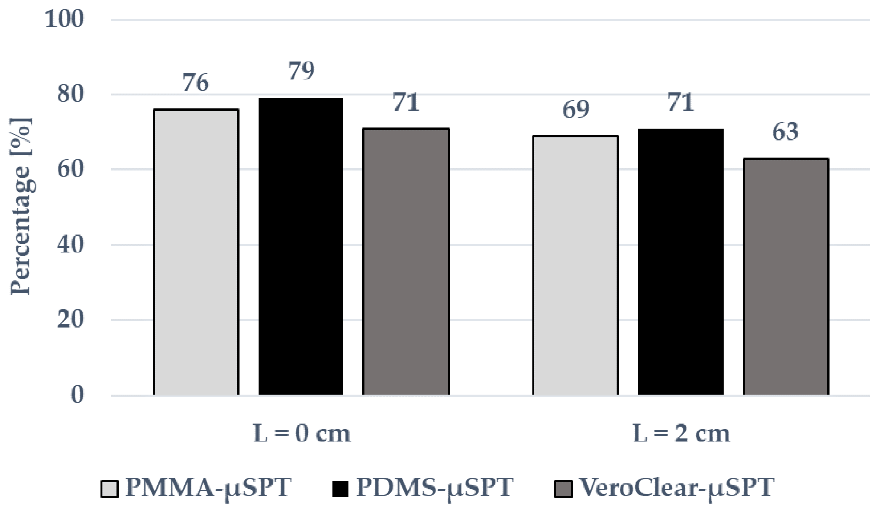
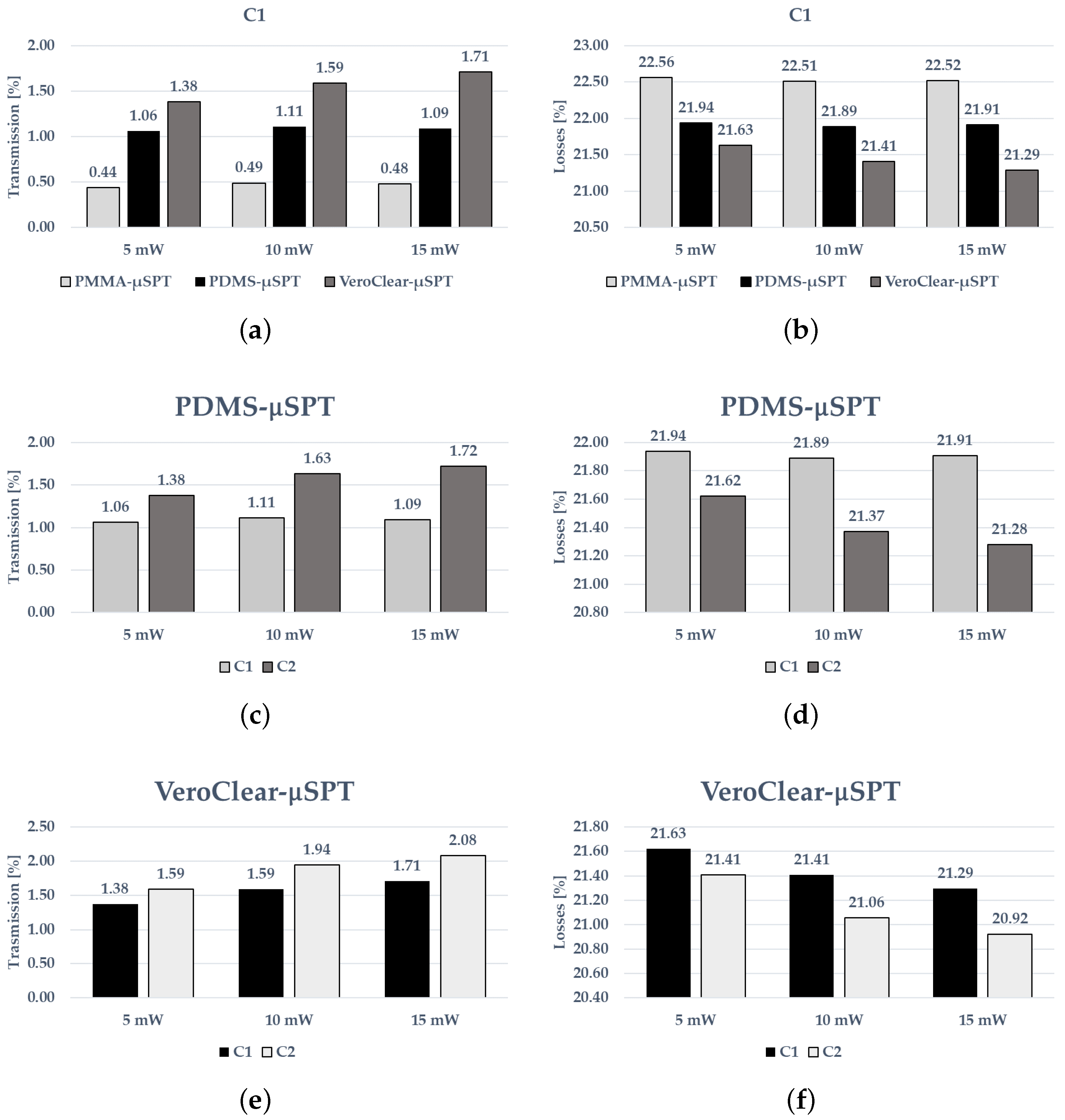
3.1. μ S P T s Optical Characterization in Comparison

The designed μ S P T was used to guide and split the light rays, considering the experimental set-up of two different configurations of the output fiber alignment, as shown in Figure 7 and described below.
  • C 1 
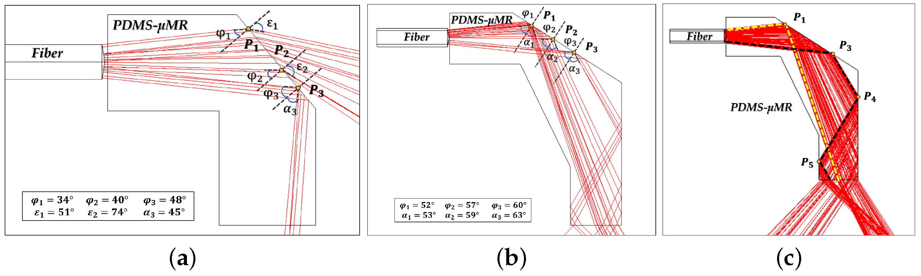
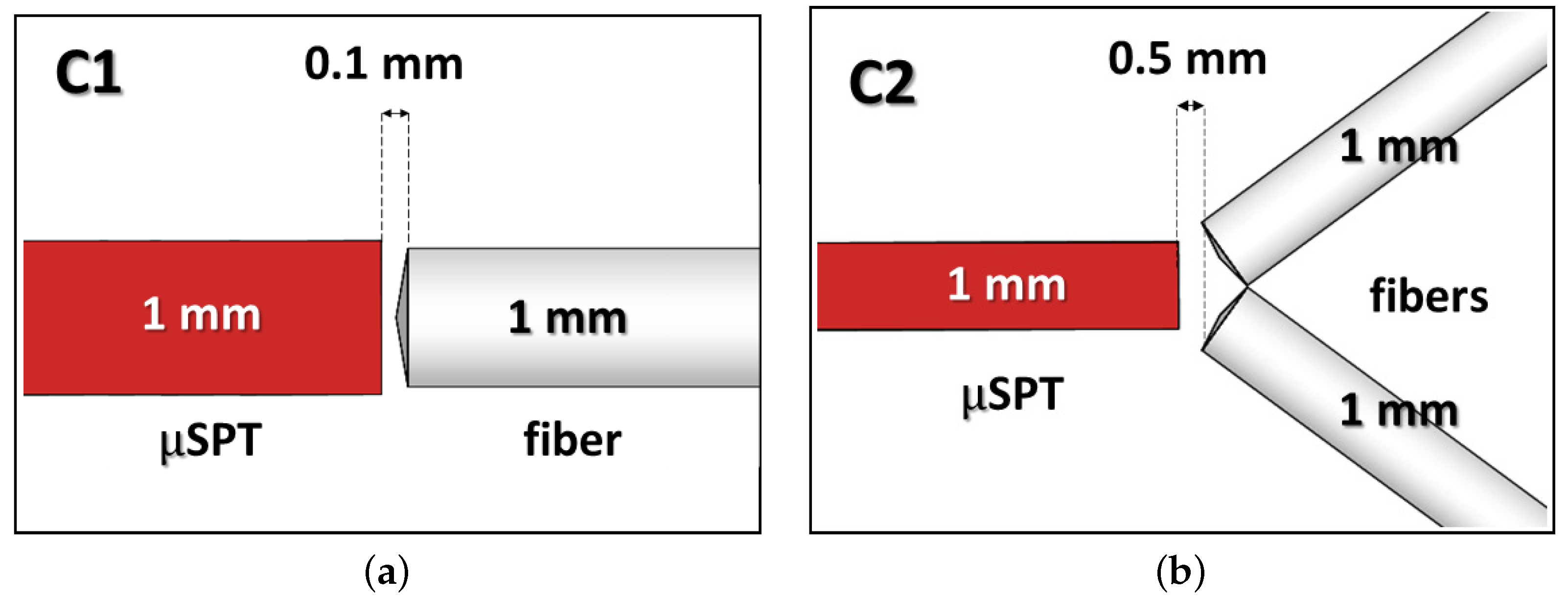
: one fiber insertion for an optical fiber was lined up with the output micro-waveguide, as in a standard configuration with d = 0.1 mm (see Figure 7a).
  • C 2 
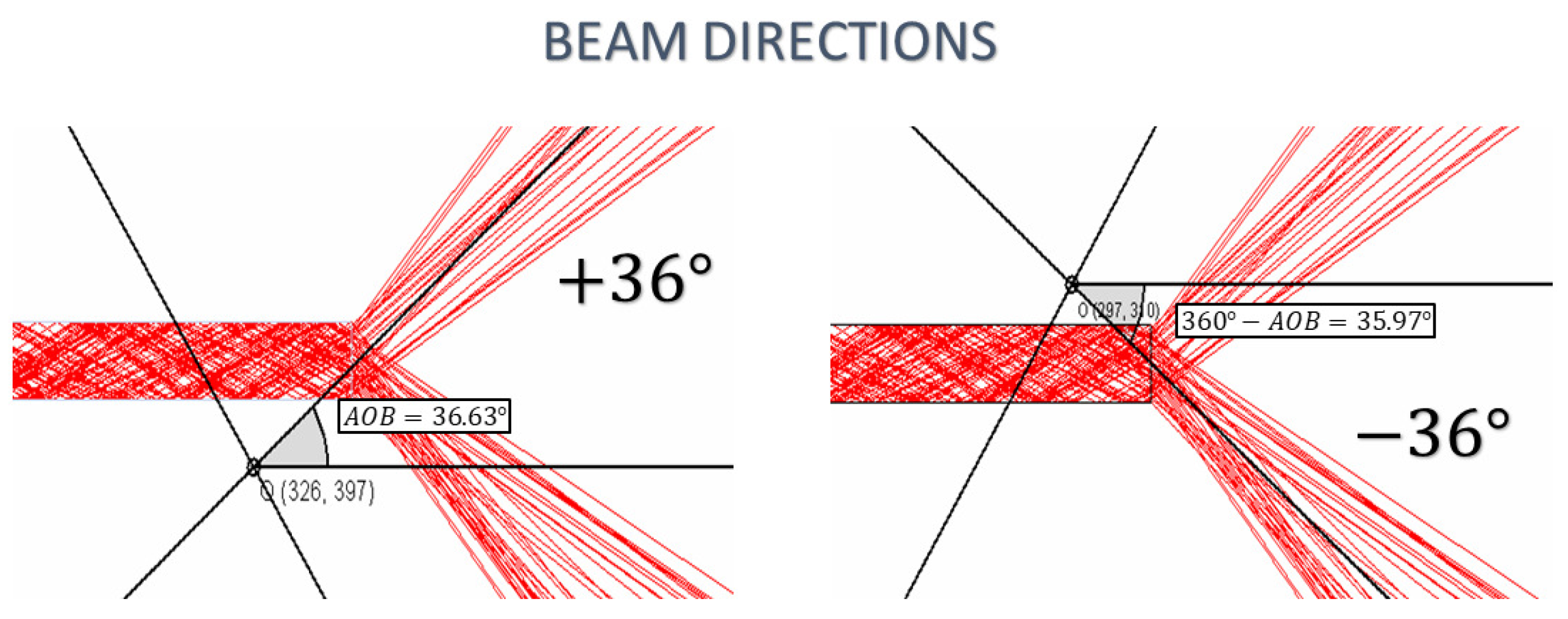
: two fiber insertions for the optical fibers were tilted at 36 , on the opposite side, with respect to the main horizontal line of the output with d = 0.5 mm (see Figure 7b).
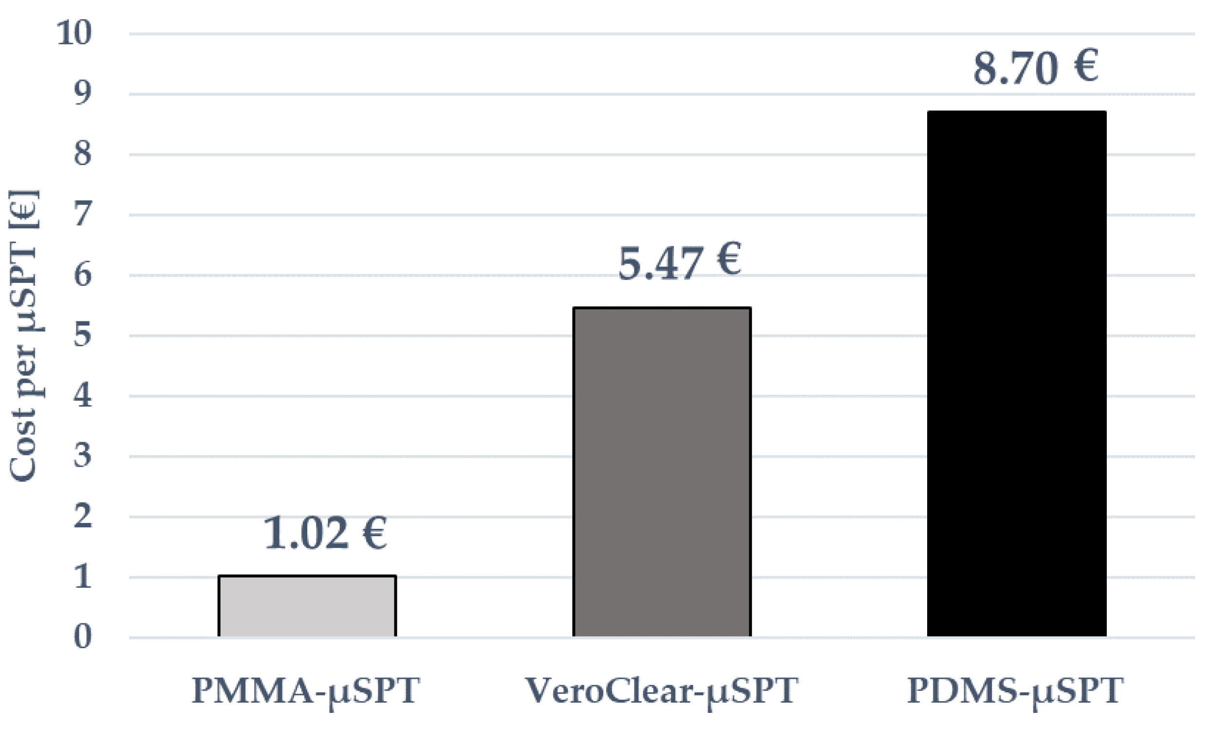
In Figure 8, the pictures of the PDMS- μ S P T (on the top), the PMMA- μ S P T (on the center), and the VeroClear- μ S P T (on the bottom) in the conditions of no-light passage and during the light-passage are shown.
Before proceeding with μ S P T characterization, a calibration of the laser-photodiode system was performed. After obtaining the input power-voltage calibration curve, the characterization of the system was carried out. The laser coupled with a 400 μm optical fiber was placed at the input to the μ S P T , varying its input power in the set { 5 , 10 , 15 } mW. At the output, the voltage values were acquired by means of the 1 mm optical fiber coupled with a photodiode. For testing the PDMS- μ S P T and the VeroClear- μ S P T , the distances d between the input–output fibers and the μ S P T were set to 100 μm and 500 μm for the first and second configurations ( C 1 ; C 2 ), respectively. It was set to 240 μm for the PMMA- μ S P T due to the limit of fabrication in the first configuration ( C 1 ). In order to understand the capability of the μ S P T s to transmit light, the values of transmission were evaluated as the ratio between the output voltage readings and the input voltage readings obtained during the calibration phase. Taking into account the losses due to the coupled fibers μ S P T in the input and output of about 77 % , obtained in [34], it was possible to calculate the losses in the μ S P T s . The histograms in Figure 9a,b report the values of transmission and losses in percentages for the experimental conditions C 1 varying the laser power in the set {5, 10, 15} mW for the three considered materials. The PDMS- μ S P T and the VeroClear- μ S P T have the same value of transmission of about 1 % and a loss percentage of 21.8 % with respect to the PMMA- μ S P T , which has a value of 0.4 % of the transmission and a loss of about 22.5 % . This difference is due to the set distance d between the input–output fibers and the μ S P T , which are lower for PDMS- μ S P T and VeroClear- μ S P T rather than PMMA- μ S P T . Furthermore, another possible limitation related to the latter is its edge roughness, which can be improved by using some specific strategies, such as surface-polishing techniques.
The histograms in Figure 9c,d report the values of the transmissions and losses (in percentages) for the experimental conditions { C 1 , C 2 } by varying the laser power in the set {5, 10, 15} mW for the PDMS- μ S P T . Figure 9e,f presents the ones related to VeroClear- μ S P T . Despite the increase in the gap d, the transmission globally detected is greater in correspondence with the configuration C 2 , with losses of about 21.4 % for both μ S P T s . Regarding the PDMS- μ S P T , looking at Figure 8a, it is possible to localize the loss areas, the brighter spots of the picture, where the holder is in contact with the PDMS- μ S P T . This confirms the possibility of splitting the information in two directions and minimizing the losses, avoiding the testing platform with direct integration of the μ S P T in a microsystem. Despite both the PMMA- μ S P T and VeroClear- μ S P T being completely surrounded by air, with the only exception for the input and output sections, with an air gap of d = 240–100 μ m in the experimental configuration C 1 , greater losses are in the input section. However, from the results obtained, VeroClear- μ S P T appears to transmit more light than the PDMS- μ S P T and the PMMA- μ S P T . Based on that results, it is possible to confirm the potential of the μ S P T ; the losses are not due to its design, but to the gaps at the insertions (d) and the surrounding material. It is possible to overcome the latter limitation, which is especially evident in the PDMS- μ S P T , by properly shielding the micro-optical components with other materials characterized by different refraction index values, thus ensuring uniformity in the light path.

3.2. μ S P T s Technologies Comparative Analysis

Once the micro-optical components were designed, manufactured, and optically characterized, a comparison analysis was carried out between the three of them. The aim was to highlight the main advantages and drawbacks related to each selected material and related manufacturing processes.
Thus, the main optical and mechanical properties, together with the key features of exploited manufacturing processes, are reported in Table 1.
By comparing the mechanical properties of the three used materials, i.e., Young’s modulus and elongation at break, it is clear that since both PMMA and VeroClear RGD810 are more rigid (Young’s modulus values ranging between 2 and 3 GPa) and less subject to deformation when compared to PDMS (5–25% elongation at the break versus 100%), the use of the former material permits realizing optical components that are capable of being handled. This feature is crucial for further integration procedures within, for example, microfluidic systems. Conversely, since PDMS is a soft material (with a Young’s modulus equal to 1.32 MPa), it can be tricky to handle during successive assembly procedures. Moving on, another advantage related to the use of the VeroClear RGD810 and PMMA is the lower number of steps for the manufacturing processes when used in combination with each other. Indeed, on the one hand, the manufacturing process for PDMS- μ S P T requires five different manufacturing steps: (i) design of the master; (ii) fabrication via 3D printing (inkjet technique) of the master; (iii) UV treatment of the master surface; (iv) PDMS casting into the master; (v) PDMS- μ S P T removing from the master. On the other hand, both the VeroClear- μ S P T and PMMA- μ S P T required two-step manufacturing processes. The manufacturing process for the VeroClear- μ S P T includes the two steps listed below: (i) design of the μ S P T ; (ii) fabrication via 3D printing (inkjet). The manufacturing process for the PMMA- μ S P T includes the following steps: (i) design of the μ S P T ; (ii) fabrication via laser cutting. Thus, both VeroClear- μ S P T and the PMMA- μ S P T can be manufactured through a faster manufacturing approach.
Moving on, focusing on PMMA microfluidic channels, their fabrication is usually realized by using a standard lithography process, a hot-embossing process, femtosecond laser processing, and the excimer laser [35,36,37,38]. Among these mentioned techniques, the one that relies on laser use is less common in modern industries because of its high costs and the difficulty in maintaining them for large-scale production. These constraints are primarily related to the use of femtosecond and excimer lasers. To overcome these issues, micro-channeling using CO2 laser processing is a one-step process that minimizes time consumption. Moreover, laser micro-processing has enabled the production of microfluidic systems with the lowest cost per unit when compared to other contemporary methods [39]. These aspects justify the decision to use the proposed manufacturing approach for the PMMA- μ S P T .
Another important aspect to take into account is that since laser cutting is a subtractive manufacturing technique, it allows working on a flat surface. However, as soon as it is necessary to design three-dimensional parts, multiple parts must be cut out and, next, molded together. Conversely, a 3D printing approach, being an additive manufacturing process, by exploiting a layer-by-layer manufacturing approach, allows for directly realizing 3D objects. Moreover, using a 3D printing process based on additive manufacturing allows for the building of objects with little or no waste. In contrast, laser cutting is a subtractive manufacturing process that generates more waste as it removes material from workpieces. The ability to fabricate a complex 3D optical component in a single 3D print run is crucial, as it eliminates post-assembly issues caused by inaccurate positioning between parts. Thus, together with the design freedom, 3D printing opens up the potential to directly fabricate complex micro-optical systems. In this sense, the 3D printing proposed manufacturing approach ensures a degree of freedom in waveguide landscapes, boosting the device’s performance. Furthermore, among other fiber fabrication techniques (such as fib milling, facet EBL, photolithography, femtosecond laser writing, and so on) proposed in the state-of-the-art, and allowing for an optical component free-design, the 3D printing approach is suitable for developing potential market products [40]. Thus, in conclusion, as the VeroClear RGD810 is a transparent PolyJetTM photopolymer, which is used in the inkjet 3D printing technique and simulates PMMA, it is the most advantageous one. Indeed, the micro-splitter characterization results showed that the VeroClear- μ S P T had the best optical performance at both C1 and C2. By considering the average values collected for the transmission parameter in correspondence of C1, evaluated by considering the whole range of power, the VeroClear- μ S P T presented an increase of about 70 % when compared to the PMMA one (by about 30 % compared to the PDMS one). This involved a reduction in the evaluated losses (average value) for the VeroClear- μ S P T of about 5 % and 2 % rather than the PMMA and PDMS ones, respectively. A similar trend was found in configuration C2. Indeed, even in this case, the average transmission value for VeroClear- μ S P T was 16 % higher than that of PDMS. So, this caused an increase in the average loss of about 1.7 % for the PDMS- μ S P T when compared to the VeroClear one.
Since the PDMS- μ S P T and VeroClear- μ S P T exhibited the best performance with the lowest loss values and were able to be tested in both configurations (C1; C2), no manufacturing constraints affected the related manufacturing processes, validating what has been said so far, i.e., a cost model was implemented. The latter allowed for the evaluation of the final cost of the PDMS- μ S P T , PMMA- μ S P T , and VeroClear- μ S P T by varying the used material and the exploited manufacturing process. In line with the model already proposed and explained in detail elsewhere [41,42], the cost parameters were categorized as material costs, machine costs, and process costs. To evaluate the final cost of the three developed μ S P T s, the input parameters that are reported in Table 2, Table 3 and Table 4, respectively, were taken into account. In detail, at first, the used raw material costs and the related quantity consumed for manufacturing the μ S P T s were considered. Since the purchase, installation, and maintenance costs of the used machines (i.e., 3D printer and laser cutter) were known, the depreciation costs were evaluated for them. Next, the power costs were estimated since the building time for each manufactured μ S P T was well-defined by varying the manufacturing approach selected. Conversely, the labor cost parameter was neglected for the direct 3D printing approach and the master–slave mold realization because the operator took only a few minutes to start the printing process and remove the parts from the building platform as soon as the 3D printing process was completed. A similar decision was made even for the laser-cutting technique since the required processing time was very low. The final evaluated costs are reported in Figure 10.
In agreement with the obtained results, the PMMA- μ S P T has a final cost of EUR 1.02, the VeroClear- μ S P T of about EUR 5.50, while it was equal to EUR 8.70 for the PDMS one. Thus, by exploiting a direct 3D printing approach it was possible to reduce the optical component cost (by about 38 % ). This result is due to the impact of the master–slave mold fabrication, which represented an additional cost to the PDMS- μ S P T itself. The PMMA optical component presented the lowest cost, which was related to the low impact of the raw material cost, to a lower cost of the laser cutting when compared to the used 3D printer, in addition to the very short processing time required for optical component manufacturing. Hence, all three of the developed μ S P T s can be considered low-cost optical components. However, even though PMMA- μ S P T represented the cheapest solution, the laser-cutting manufacturing approach presented some fabrication limitations. Conversely, the higher final costs evaluated for both the PDMS and VeroClear μ S P T s have interesting optical properties and good repeatability. Based on the discussed results, the proposed manufacturing approach and the selected materials are suitable for mass production of the developed micro-optical components.

4. Conclusions

In this paper, the design and realization of a μ S P T , an optical component capable of splitting light into two paths, was presented. In microfluidics, it is important to confine and transport the light as close as possible to the sample, by guiding it into a small volume of the microfluidic channel and acquiring the emitted/transmitted radiation. The presented μ S P T is able to fulfill this purpose and it was realized by exploiting three different low-cost technologies. Three materials were used for its fabrication: poly-dimethyl-siloxane (PDMS), poly(methyl methacrylate) (PMMA), and VeroClear RGD810. A 3D printing master–slave fabrication protocol was used with PDMS, a direct 3D printing approach was used with VeroClear, and a laser cutting procedure was used with PMMA. The three technologies investigated were compared; they presented very good results in terms of cost quality. In particular, the results obtained proved the high potential of the proposed fabrication protocols, based on low-cost technologies, for the realization of micro-optical components, which could also be easily integrated with microfluidics systems for Lab-on-a-Chip applications. The results presented show the potential of creating micro-optical paths inside microsystems; an example can be found in a micro-optofluidics application discussed in [29], where a micro-optical component (a micro-waveguide) was integrated into a micro-optofluidic device to detect chemical fluids and for cell detection. Furthermore, in [43], a simple micro-optofluidic device with no micro-waveguide integrated was realized in 3D printing, exploiting new low-cost technologies, such as projection micro-stereolithography. The device was designed for slug flow detection in micro-channels. Indeed, by functionalizing the μ S P T s with a noble metal nanofilm through proper deposition processes, and integrating them into micro-optofluidic devices with a tailored refractive index value, it would be possible to develop devices suitable for molecular diagnostics [44], clinical diagnostics [45,46], toxins, small molecule sensing [47,48,49], and mechano-optical applications [49].

Author Contributions

Conceptualization G.S., L.S., A.E.O., G.C., M.K.-K. and M.B.; methodology G.S., L.S., A.E.O., G.C., M.K.-K. and M.B.; validation G.S., L.S., A.E.O., G.C., M.K.-K. and M.B.; writing G.S., L.S., A.E.O., G.C., M.K.-K. and M.B. All authors have read and agreed to the published version of the manuscript.

Funding

The research activity was partially supported by the University of Catania under grant scheme PIACERI with project MAF-moF “Materiali multifunzionali per dispositivi micro-optofluidici” and partially funded by the European Union (NextGeneration EU) through the MUR-PNRR project SAMOTHRACE (ECS00000022).

Institutional Review Board Statement

Not applicable.

Informed Consent Statement

Not applicable.

Data Availability Statement

The CAD source file is available online at http://www.dees.unict.it/mbucolo/index.php/resources (accessed on 9 March 2023).

Conflicts of Interest

The authors declare no conflict of interest.

References

  1. Bliss, C.L.; McMullin, J.N.; Backhouse, C.J. Rapid fabrication of a microfluidic device with integrated optical waveguides for DNA fragment analysis. Lab Chip 2007, 7, 1280–1287. [Google Scholar] [CrossRef]
  2. Kuswandi, B.; Huskens, J.; Verboom, W. Optical sensing systems for microfluidic devices: A review. Anal. Chim. Acta 2007, 601, 141–155. [Google Scholar] [CrossRef] [PubMed]
  3. Yin, D.; Lunt, E.J.; Rudenko, M.I.; Deamer, D.W.; Hawkins, A.R.; Schmidt, H. Planar optofluidic chip for single particle detection, manipulation, and analysis. Lab Chip 2007, 7, 1171–1175. [Google Scholar] [CrossRef] [PubMed]
  4. Applegate, R.W., Jr.; Squier, J.; Vestad, T.; Oakey, J.; Marr, D.W.; Bado, P.; Said, A.A. Microfluidic sorting system based on optical waveguide integration and diode laser bar trapping. Lab Chip 2006, 6, 422–426. [Google Scholar] [CrossRef]
  5. Meddens, M.B.; Liu, S.; Finnegan, P.S.; Edwards, T.L.; James, C.D.; Lidke, K.A. Single objective light-sheet microscopy for high-speed whole-cell 3D super-resolution. Biomed. Opt. Express 2016, 7, 2219–2236. [Google Scholar] [CrossRef] [PubMed] [Green Version]
  6. Paiè, P.; Martínez Vázquez, R.; Osellame, R.; Bragheri, F.; Bassi, A. Microfluidic based optical microscopes on chip. Cytom. Part A 2018, 93, 987–996. [Google Scholar] [CrossRef]
  7. Hung, T.Q.; Chin, W.H.; Sun, Y.; Wolff, A.; Bang, D.D. A novel lab-on-chip platform with integrated solid phase PCR and Supercritical Angle Fluorescence (SAF) microlens array for highly sensitive and multiplexed pathogen detection. Biosens. Bioelectron. 2017, 90, 217–223. [Google Scholar] [CrossRef]
  8. Watts, B.R.; Zhang, Z.; Xu, C.Q.; Cao, X.; Lin, M. Integration of optical components on-chip for scattering and fluorescence detection in an optofluidic device. Biomed. Opt. Express 2012, 3, 2784–2793. [Google Scholar] [CrossRef]
  9. Hubner, J.; Jorgensen, A.M.; Anhoj, T.A.; Zauner, D.A. Integrated optical systems for lab-on-a-chip applications, Integrated Optics: Devices, Materials, and Technologies IX. Int. Soc. Opt. Photonics 2005, 5728, 269–277. [Google Scholar]
  10. Mogensen, K.B.; El-Ali, J.; Wolff, A.; Kutter, J.P. Integration of polymer waveguides for optical detection in microfabricated chemical analysis systems. Appl. Opt. 2003, 42, 4072–4079. [Google Scholar] [CrossRef]
  11. Mogensen, K.B.; Friis, P.; Hübner, J.; Petersen, N.; Jørgensen, A.M.; Telleman, P.; Kutter, J.P. Ultraviolet transparent silicon oxynitride waveguides for biochemical microsystems. Opt. Lett. 2001, 26, 716–718. [Google Scholar] [CrossRef] [PubMed]
  12. Mazurczyk, R.; Vieillard, J.; Bouchard, A.; Hannes, B.; Krawczyk, S. A novel concept of the integrated fluorescence detection system and its application in a lab-on-a-chip microdevice. Sensors Actuators Chem. 2006, 118, 11–19. [Google Scholar] [CrossRef]
  13. Teitelbaum, M.E.; Nair, R.; O’Brien, D.J.; Wetzel, E.D.; Goossen, K.W. Cost-effective integration of plastic optical fiber and total internal reflection mirrors in printed circuit boards for parallel optical interconnects. Opt. Eng. 2010, 49, 065401. [Google Scholar] [CrossRef]
  14. Cook, K.; Canning, J.; Leon-Saval, S.; Reid, Z.; Hossain, M.A.; Comatti, J.E.; Peng, G.D. Air-structured opti- cal fiber drawn from a 3D-printed preform. Opt. Lett. 2015, 40, 3966–3969. [Google Scholar] [CrossRef] [Green Version]
  15. Luo, Y.; Canning, J.; Zhang, J.; Peng, G.D. Toward optical fibre fabrication using 3D printing technology. Opt. Fiber Technol. 2020, 58, 102299. [Google Scholar] [CrossRef]
  16. Chan, H.N.; Tan, M.J.A.; Wu, H. Point-of-care testing: Applications of 3D printing. Lab Chip 2017, 17, 2713–2739. [Google Scholar] [CrossRef]
  17. Hwang, Y.; Paydar, O.H.; Candler, R.N. 3D printed molds for non-planar PDMS microfluidic channels. Sensors Actuators A Phys. 2015, 226, 137–142. [Google Scholar] [CrossRef]
  18. Palmara, G.; Frascella, F.; Roppolo, I.; Chiappone, A.; Chiadò, A. Functional 3D printing: Approaches and bioapplications. Biosens. Bioelectron. 2021, 175, 112849. [Google Scholar] [CrossRef]
  19. Gold, K.; Gaharwar, A.K.; Jain, A. Emerging trends in multiscale modeling of vascular pathophysiology: Organ-on-a-chip and 3D printing. Biomaterials 2019, 196, 2–17. [Google Scholar] [CrossRef]
  20. Yazdi, A.A.; Popma, A.; Wong, W.; Nguyen, T.; Pan, Y.; Xu, J. 3D printing: An emerging tool for novel microfluidics and lab-on-a-chip applications. Microfluid. Nanofluidics 2016, 20, 50. [Google Scholar] [CrossRef]
  21. Bhargava, K.C.; Thompson, B.; Malmstadt, N. Discrete elements for 3D microfluidics. Proc. Natl. Acad. Sci. USA 2014, 111, 15013–15018. [Google Scholar] [CrossRef] [PubMed] [Green Version]
  22. Zhao, H.; Chin, L.K.; Shi, Y.; Liu, P.Y.; Zhang, Y.; Cai, H.; Liu, A.Q. Continuous optical sorting of nanoscale biomolecules in integrated microfluidic-nanophotonic chips. Sensors Actuators B Chem. 2021, 331, 129428. [Google Scholar] [CrossRef]
  23. Tang, X.; Liang, S.; Li, R. Design for controllable optofluidic beam splitter. Photonics Nanostructures Fundam. Appl. 2016, 18, 23–30. [Google Scholar] [CrossRef]
  24. Mogensen, K.B.; Kwok, Y.C.; Eijkel, J.C.; Petersen, N.J.; Manz, A.; Kutter, J.P. A microfluidic device with an integrated waveguide beam splitter for velocity measurements of flowing particles by Fourier transformation. Anal. Chem. 2003, 75, 4931–4936. [Google Scholar] [CrossRef]
  25. Vélez, P.; Su, L.; Grenier, K.; Mata-Contreras, J.; Dubuc, D.; Martín, F. Microwave microfluidic sensor based on a microstrip splitter/combiner configuration and split ring resonators (SRRs) for dielectric characterization of liquids. IEEE Sens. J. 2017, 17, 6589–6598. [Google Scholar] [CrossRef] [Green Version]
  26. Nguyen, N.T.; Kong, T.F.; Goh, J.H.; Low, C.L.N. A micro optofluidic splitter and switch based on hydrodynamic spreading. J. Micromech. Microeng. 2007, 17, 2169. [Google Scholar] [CrossRef]
  27. Cleary, A.; Garcia-Blanco, S.; Glidle, A.; Aitchison, J.S.; Laybourn, P.; Cooper, J.M. An integrated fluorescence array as a platform for lab-on-a-chip technology using multimode interference splitters. IEEE Sens. J. 2005, 5, 1315–1320. [Google Scholar] [CrossRef]
  28. Cairone, F.; Gagliano, S.; Carbone, D.C.; Recca, G.; Bucolo, M. Micro-optofluidic switch realized by 3D printing technology. Microfluid. Nanofluidics 2016, 20, 61. [Google Scholar] [CrossRef]
  29. Cairone, F.; Davi, S.; Stella, G.; Guarino, F.; Recca, G.; Cicala, G.; Bucolo, M. 3D-Printed micro-optofluidic device for chemical fluids and cells detection. Biomed. Microdevices 2020, 22, 1–10. [Google Scholar] [CrossRef]
  30. Maia, J.M.; Amorim, V.A.; Alexandre, D.; Marques, P.V. Real-time optical monitoring of etching reaction of microfluidic channel fabricated by femtosecond laser direct writing. J. Light. Technol. 2017, 35, 291–2298. [Google Scholar] [CrossRef] [Green Version]
  31. Sugioka, K.; Cheng, Y. Femtosecond laser processing for optofluidic fabrication. Lab Chip 2012, 12, 3576–3589. [Google Scholar] [CrossRef] [PubMed]
  32. Vazquez, R.M.; Osellame, R.; Nolli, D.; Dongre, C.; Van Den Vlekkert, H.; Ramponi, R.; Cerullo, G. Integration of femtosecond laser written optical waveguides in a lab-on-chip. Lab Chip 2009, 9, 91–96. [Google Scholar] [CrossRef] [PubMed]
  33. Liga, A.; Morton, J.A.; Kersaudy-Kerhoas, M. Safe and cost-effective rapid-prototyping of multilayer PMMA microfluidic devices. Microfluid. Nanofluidics 2016, 20, 1–12. [Google Scholar] [CrossRef] [Green Version]
  34. Cairone, F.; Gallo Afflitto, F.; Stella, G.; Cicala, G.; Ashour, M.; Kersaudy-Kerhoas, M.; Bucolo, M. Micro-Optical Waveguides Realization by Low-Cost Technologies. Micro 2022, 2, 123–136. [Google Scholar] [CrossRef]
  35. Fernández-Pradas, J.; Florian, C.; Caballero-Lucas, F.; Morenza, J.; Serra, P. Femtosecond Laser Ablation of Polymethyl-Methacrylate with High Focusing Control. Appl. Surf. Sci. 2013, 278, 185–189. [Google Scholar] [CrossRef]
  36. Becker, H.; Locascio, L.E. Polymer Microfluidic Devices. Talanta 2002, 56, 267–287. [Google Scholar] [CrossRef] [PubMed]
  37. Mathur, A.; Roy, S.S.; Tweedie, M.; Mukhopadhyay, S.; Mitra, S.; McLaughlin, J. Characterisation of PMMA Microfluidic Channels and Devices Fabricated by Hot Embossing and Sealed by Direct Bonding. Curr. Appl. Phys. 2009, 9, 1199–1202. [Google Scholar] [CrossRef]
  38. Chang, T.C.; Molian, P.A. Excimer Pulsed Laser Ablation of Polymers in Air and Liquids for Micromachining Applications. J. Manuf. Process. 1999, 1, 1–17. [Google Scholar] [CrossRef]
  39. Prakash, S.; Kumar, S. Fabrication of microchannels on transparent PMMA using CO2 Laser (10.6 μm) for microfluidic applications: An experimental investigation. Int. J. Precis. Eng. Manuf. 2015, 16, 361–366. [Google Scholar] [CrossRef]
  40. Meng, Y.; Chen, Y.; Lu, L.; Ding, Y.; Cusano, A.; Fan, J.A.; Ni, X. Optical meta-waveguides for integrated photonics and beyond. Light Sci. Appl. 2021, 16, 235. [Google Scholar] [CrossRef]
  41. Cennamo, N.; Saitta, L.; Tosto, C.; Arcadio, F.; Zeni, L.; Fragalá, M.E.; Cicala, G. Microstructured Surface Plasmon Resonance Sensor Based on Inkjet 3D Printing Using Photocurable Resins with Tailored Refractive Index. Polymers 2021, 13, 2518. [Google Scholar] [CrossRef]
  42. Saitta, L.; Arcadio, F.; Celano, G.; Cennamo, N.; Zeni, L.; Tosto, C.; Cicala, G. Design and manufacturing of a surface plasmon resonance sensor based on inkjet 3D printing for simultaneous measurements of refractive index and temperature. Int. J. Adv. Manuf. Technol. 2023, 124, 2261–2278. [Google Scholar] [CrossRef]
  43. Saitta, L.; Celano, G.; Cicala, G.; Fragalà, M.E.; Stella, G.; Barcellona, M.; Tosto, C.; Bucolo, M. Projection micro-stereolithography versus master–slave approach to manufacture a micro-optofluidic device for slug flow detection. Int. J. Adv. Manuf. Technol. 2022, 120, 4443–4460. [Google Scholar] [CrossRef]
  44. Tang, L.; Li, J. Plasmon-based colorimetric nanosensors for ultrasensitive molecular diagnostics. ACS Sens. 2017, 2, 857–875. [Google Scholar] [CrossRef]
  45. Masson, J.F. Surface Plasmon Resonance Clinical Biosensors for Medical Diagnostics. ACS Sens. 2017, 2, 16–30. [Google Scholar] [CrossRef] [PubMed]
  46. Yanase, Y.; Hiragun, T.; Ishii, K.; Kawaguchi, T.; Yanase, T.; Kawai, M.; Sakamoto, K.; Hide, M. Surface Plasmon Resonance for Cell-Based Clinical Diagnosis. Sensors 2014, 14, 4948–4959. [Google Scholar] [CrossRef]
  47. Hodnik, V.; Anderluh, G. Toxin detection by surface plasmon resonance. Sensors 2009, 9, 1339–1354. [Google Scholar] [CrossRef]
  48. Mitchell, J. Small molecule immunosensing using surface plasmon resonance. Sensors 2010, 10, 7323–7346. [Google Scholar] [CrossRef] [Green Version]
  49. García-Merino, J.A.; Torres-Torres, D.; Carrillo-Delgado, C.; Trejo-Valdez, M.; Torres-Torres, C. Optofluidic and strain measurements induced by polarization-resolved nanosecond pulses in gold-based nanofluids. Optik 2019, 182, 443–451. [Google Scholar] [CrossRef]
Figure 1. Design of the micro-splitter ( μ S P T ): (a) a micro-mirror ( μ M R ) in-between two micro-waveguides ( μ W G s ) of length L. (b) For L = 0 cm , the design of the μ S P T matches with that of the μ M R and consists of an input and output surface and two surfaces M 1 and M 2 , respectively, tilted at the angles { β , γ } .
Micro 03 00023 g001
Figure 2. Optimal values of { β , γ } identified by ray tracing simulations. (a) The design of PDMS- μ M R with the surface M 1 angled by { β = 45 } . (b) The design of PDMS- μ M R including both surfaces { M 1 , M 2 } angled by { β = 57 . 35 , γ = 26 } . (c) Complete path of the rays inside the PDMS- μ M R .
Micro 03 00023 g002
Figure 3. Histogram of the percentage of rays, obtained by ray-tracing simulations, reaching the output fiber surfaces for two different lengths L = { 0 ; 2 } cm and for the PMMA- μ S P T , the PDMS- μ S P T , and the VeroClear- μ S P T . Bar errors have not been added because they were narrower than the bar height.
Micro 03 00023 g003
Figure 4. The two paths of the light beam after being bent by the μ M R . An angle of about 36 was identified with respect to the main direction of the light.
Micro 03 00023 g004
Figure 5. Steps in the realization of the two testing platforms used for the characterization of the (a) PDMS- μ S P T and (b) VeroClear- μ S P T . In both figures, on the left, the holder is designed to support the micro-optical component and the scheme of the holder with the top and bottom layers is used for the fiber alignment; on the right the photo of the complete micro-optical systems.
Micro 03 00023 g005
Figure 6. (a) The flow chart and (b) the picture of the experimental set-up used for the micro-optical characterization of the PDMS- μ S P T . At the input, the laser source is connected to a multi-mode optical fiber. At the output, a fiber is coupled with a photo-diode and a digital oscilloscope is used for the reading. Both fibers are aligned with the μ S P T .
Micro 03 00023 g006
Figure 7. Two different configurations of light acquisition between the output fibers and the μ S P T . (a) Configuration 1 (C1) shows one optical fiber placed horizontally with respect to the μ S P T . (b) Configuration 2 (C2) shows two optical fibers tilted, in opposite directions, at 36 , with respect to the μ S P T .
Micro 03 00023 g007
Figure 8. The pictures of the μ S P T in the no-light passage and during light-passage conditions. The top shows (a) the PDMS- μ S P T , the center shows (b) the PMMA- μ S P T , and the bottom shows (c) the VeroClear- μ S P T .
Micro 03 00023 g008
Figure 9. Histograms of (a) transmission and (b) losses for the the PMMA- μ S P T , the PDMS- μ S P T and the VeroClear- μ S P T in the configuration C 1 . Comparison of the (c) transmission and (d) losses with the PDMS- μ S P T in the configurations { C 1 , C 2 } . Comparison of the (e) transmission and (f) losses with the VeroClear- μ S P T in the configurations { C 1 , C 2 } . The laser power at the input was varied at {5; 10; 15} mW. Bar errors were not added because they were strongly narrower than the bar height.
Micro 03 00023 g009
Figure 10. Evaluated final cost per unit for the PMMA- μ S P T , the VeroClear- μ S P T and the PDMS- μ S P T .
Micro 03 00023 g010
Table 1. Comparative analysis between the PDMS- μ S P T , the PMMA- μ S P T , and the VeroClear- μ S P T in terms of optical properties, mechanical properties, and manufacturing process.
MaterialAverage Measured TransmissionAverage Measured LossesYoung’s ModulusElongation at BreakManufacturing ProcessSteps of Manufacturing Process
PDMS1.09 ± 0.0321.91 ± 0.031.32 MPa100%Master–slave approach5
PMMA0.47 ± 0.0322.53 ± 0.032.9 GPa5%Laser cutting2
VeroClear RGD8101.56 ± 0.1721.44 ± 0.172–3 GPa10–25%3D printing2
Table 2. Cost model input parameters considered for the PDMS- μ S P T .
UnitValue
MaterialVero PureWhite RGD837EUR (€)/kg225.50
FullCure705EUR (€)/kg126.74
SYLGARDTM 184 Silicone Elastomer KitEUR (€)/kg236.97
PartModelkg0.012
Supportkg0.007
Printing Timeh0.40
MachineDepreciation CostEUR (€)/h10.00
ProcessPower CostEUR (€)/kWh0.10
LaborEUR (€)/h30.00
Table 3. Cost model input parameters considered for the PMMA- μ S P T .
UnitValue
MaterialPMMA sheet 2 mm thickEUR (€)/mm20.000063
PMMA sheet 0.2 mm thickEUR (€)/mm20.00015
PartPMMA sheet ( 55 × 77 × 2 ) mm3EUR (€)0.135
PMMA sheet ( 55 × 77 × 0.2 ) mm3EUR (€)0.65
Processing Timeh0.03
MachineDepreciation CostEUR (€)/h2.00
ProcessPower CostEUR (€)/kWh0.10
LaborEUR (€)/h16.00
Table 4. Cost model input parameters considered for the VeroClear- μ S P T .
UnitValue
MaterialVeroClear RGD810EUR (€)/kg393.11
FullCure705EUR (€)/kg126.74
PartModelkg0.003
Supportkg0.002
Printing Timeh0.37
MachineDepreciation CostEUR (€)/h10.00
ProcessPower CostEUR (€)/kWh0.10
LaborEUR (€)/h30.00
Disclaimer/Publisher’s Note: The statements, opinions and data contained in all publications are solely those of the individual author(s) and contributor(s) and not of MDPI and/or the editor(s). MDPI and/or the editor(s) disclaim responsibility for any injury to people or property resulting from any ideas, methods, instructions or products referred to in the content.

