
Fabrication and Characterization of Pre-Defined Few-Layer Graphene
by
 , , , , and
Tingting Wang
1,† ,
,
Liangguang Jia
1,†,
Quanzhen Zhang
1,
Ziqiang Xu
1,
Zeping Huang
1,
Peiwen Yuan
1,
Baofei Hou
1,
Xuan Song
1,
Kaiqi Nie
2,
Chen Liu
2,
Jiaou Wang
2,
Huixia Yang
1,
Liwei Liu
1,
Teng Zhang
1,* and
Yeliang Wang
1 1
MIIT Key Laboratory for Low-Dimensional Quantum Structure and Devices, School of Integrated Circuits and Electronics, Beijing Institute of Technology, Beijing 100081, China
2
Beijing Synchrotron Radiation Facility, Institute of High Energy Physics, The Chinese Academy of Sciences, Beijing 100049, China
*
Author to whom correspondence should be addressed.
†
These authors contributed equally to this work.
Physchem 2023, 3(1), 13-21; https://doi.org/10.3390/physchem3010002
Submission received: 20 October 2022
/
Revised: 11 December 2022
/
Accepted: 13 December 2022
/
Published: 21 December 2022
(This article belongs to the Section Surface Science)
Abstract
:Graphene is one of the most well-known two-dimensional (2D) materials that has attracted significant interest due to its unique electrical and optical properties. Being a van der Waals substrate, the fabrication of few-layered graphene by stacking a pre-defined number of graphene monolayers is essential in the field. The thickness can influence the interface interaction and therefore tune the surface electronic properties. In the study, we demonstrate a bottom-up synthesis of pre-defined few-layer graphene on SiC substrate using the thermal decomposition method and carefully characterize its thickness by the non-damageable synchrotron-radiation-based X-ray photo-electron spectroscopy (SR-XPS). By varying the photon energy, we acquire different probe depths, resulting in the different intensity ratios of graphene to SiC substrate, which is then used to estimate the thickness of the few-layer graphene. Our calculation demonstrates that the thermal decomposition method in the study can repeatedly fabricate graphene samples with expected thickness. We further compare the obtained few-layer graphene to the single-layer graphene and HOPG using the scanning tunneling microscopy (STM) technique. Our work provides accurate methods for fabricating and characterizing pre-defined few-layer graphene, providing essential knowledge in future graphene-based thin film electronics.
1. Introduction
Since graphene was first isolated in 2004 [1], 2D materials have attracted the intensive interest of numerous scientists worldwide. Graphene, as the representative of the 2D material family, has many unique electrical and optical properties and therefore attracts the attention of researchers. Graphene is an atomically thin layer of sp2 hybridized carbon atoms that shows prominent electronic [2], optical [3,4], and mechanical properties [5,6,7]. There have been many studies on graphene preparation methods in recent years, such as mechanical exfoliation [8,9], liquid exfoliation [10,11,12,13], chemical vapor deposition (CVD) [14,15], and thermal decomposition [16,17]. Mechanical exfoliation is the most convenient way to obtain new, atomically flat surfaces of layered graphene. Mechanical exfoliation is easy to perform as it only needs tape and highly oriented pyrolytic graphene (HOPG).
In this case, 2D materials are usually atomically thin monolayers. In the case of multi-layer graphene, the number of layers can significantly influence its physical properties [18]. In fact, the number of graphene layers can be used to tune the surface electronic property [19,20,21,22,23]. Therefore, it is significant to precisely control and measure the layers of graphene. Many methods can be used to estimate the thickness of graphene, including optical contrast, Raman scattering [24,25], and scanning probe microscopy techniques [26]. Generally speaking, Raman spectroscopy has a drawback that requires the cleanness of the graphene sample with few structural/chemical defects and is more often applied to few-layer (N < 4) samples than to thick samples. On the other hand, using scanning probe microscopy techniques (such as AFM) to detect the sample thickness has the disadvantage that AFM has proven to be inaccurate for few-layer graphene.
In our work, we use the thermal deposition method to prepare the graphene on a 4H-SiC substrate. The fabrication method in the study ensures that the few-layer graphene has a pre-defined average thickness of about 5 layers (15 Å). Using the scanning tunneling microscopy technique (STM), we characterize the sample morphology with an atomic resolution and compare the few-layer graphene (grown on 4H-SiC) with single-layer graphene (grown on 6H-SiC) and thick graphene (HOPG). The thickness of the few-layer graphene is then carefully characterized by synchrotron-radiation-based X-ray photo-electron spectroscopy (SR-PES). By changing the photon energy, we control the inelastic mean free path and therefore change the intensity ratio of peaks coming from graphene and SiC substrate. We show that the thickness estimation method using SR-XPS is accurate without any sample damage. Our study confirms the preparation method of pre-defined few-layer graphene of about 5 layers on 4H-SiC, which offers a specific few-layer graphene substrate enabling possible graphene device applications.
2. Materials and Methods
2.1. Few-Layered Graphene: Sample Preparation
The graphene layers are grown on a 4H-SiC (0001) silicon carbide substrate by thermal decomposition. The SiC is previously degassed at 700 °C for 10 h by applying current to both ends of the sample holder, keeping the pressure of the chamber at 10−9 mbar. The degassing procedure ensures the removal of impurities absorbed on the surface. After degassing, we increase the direct heating current to 1.21 A (power reaches 26 W). The color of SiC becomes brighter and brighter until it glows orange-white light. Using a pyrometer (infrared temperature measurement), we acquire the temperature of 4H-SiC, which is about 1300 °C. Due to the increasing temperature, the pressure in the chamber will be as high as 10−8 mbar. We then keep the sample at this temperature for approximately an hour. At this stage, C-Si bonding on the surface is decomposed. After the decomposition, the silicon atoms escape from the surface while the C atoms are left on the surface and reconstructed, forming graphene layers on top of the SiC substrate. The 1st layer of the reconstruction of the C atoms is a complex buffer layer that consists of a non-conducting, carbon-rich interfacial layer. The buffer layer, different from graphene, partly has covalent bonding with the bulk SiC [26,27]. The scheme demonstrating the formation process of graphene on SiC substrate is shown in Figure 1.
After the formation of the buffer layer, graphene starts to grow on the buffer layer on the SiC surface. The force between the buffer layer and graphene layers is dominated by the weak vdWs interaction. During the graphene-forming process, graphene grows fast in the first 10 min and slows down gradually. The graphene growth usually stops within one hour (starting from the annealing procedure) [27]. This preparation procedure can successfully and repetitively fabricate the pre-defined few-layer graphene on SiC substrate. The sample structure is illustrated in Figure 2.
Compared to other conventional few-layer graphene preparation techniques, the thermal decomposition method has the following advantage. The graphene can be directly obtained on SiC substrate, so no transfer is required. Thermal decomposition of SiC has been intensively studied lately as a promising route for obtaining highly reproducible and homogenous large-area graphene for electronic applications [28].
2.2. Characterization Methods
After the preparation, the sample is characterized by STM in an ultrahigh vacuum (UHV) condition (with base pressure in low 10−10 mbar) operated at room temperature [29]. The measurement is performed in the constant current mode to gain the morphology information of the samples.
The thickness of the few-layered graphene is characterized by SR-XPS. The experiment is carried out at the photoemission beamline at the Beijing Synchrotron Radiation Facility (BSRF). The binding energy of the photo-electron spectra is calibrated using the Au 4f7/2 photo-electron line of a gold reference sample. The resolution of all spectra is better than 600 meV.
In our experiment, we calculate the thickness of graphene through SR-XPS. This non-damageable thickness estimation method is briefly introduced in the following. In the synchrotron radiation facility, we can change the photon energy (hv) and therefore change the inelastic mean free path (IMFP) [30]. The related effective attenuation length (EAL) is also changing with the IMFP. The IMFP and EAL are particularly important to gain information on adsorbate film thickness. In this regard, we can apply the so-called “attenuation method” to determine the adsorbate thickness [31]. Usually, the attenuation method needs at least two samples prepared in succession. One substrate sample (SiC in our case) and then grow films on top of it (graphene/SiC). It is because that the method requires information on the pure substrate (sample 1) and information on the adsorbate/substrate (sample 2) [32]. Here, we improved the standard “attenuation method” by using the idea introduced by Mikoushkin et al., so that only one sample is needed [33]. Instead of using two samples, in the study, we use the ratio of the adsorbate (peak intensity of graphene and the buffer layer) and substrate (peak intensity of the SiC) to obtain the thickness information.
3. Results and Discussions
3.1. Characterization of Few-Layer Graphene
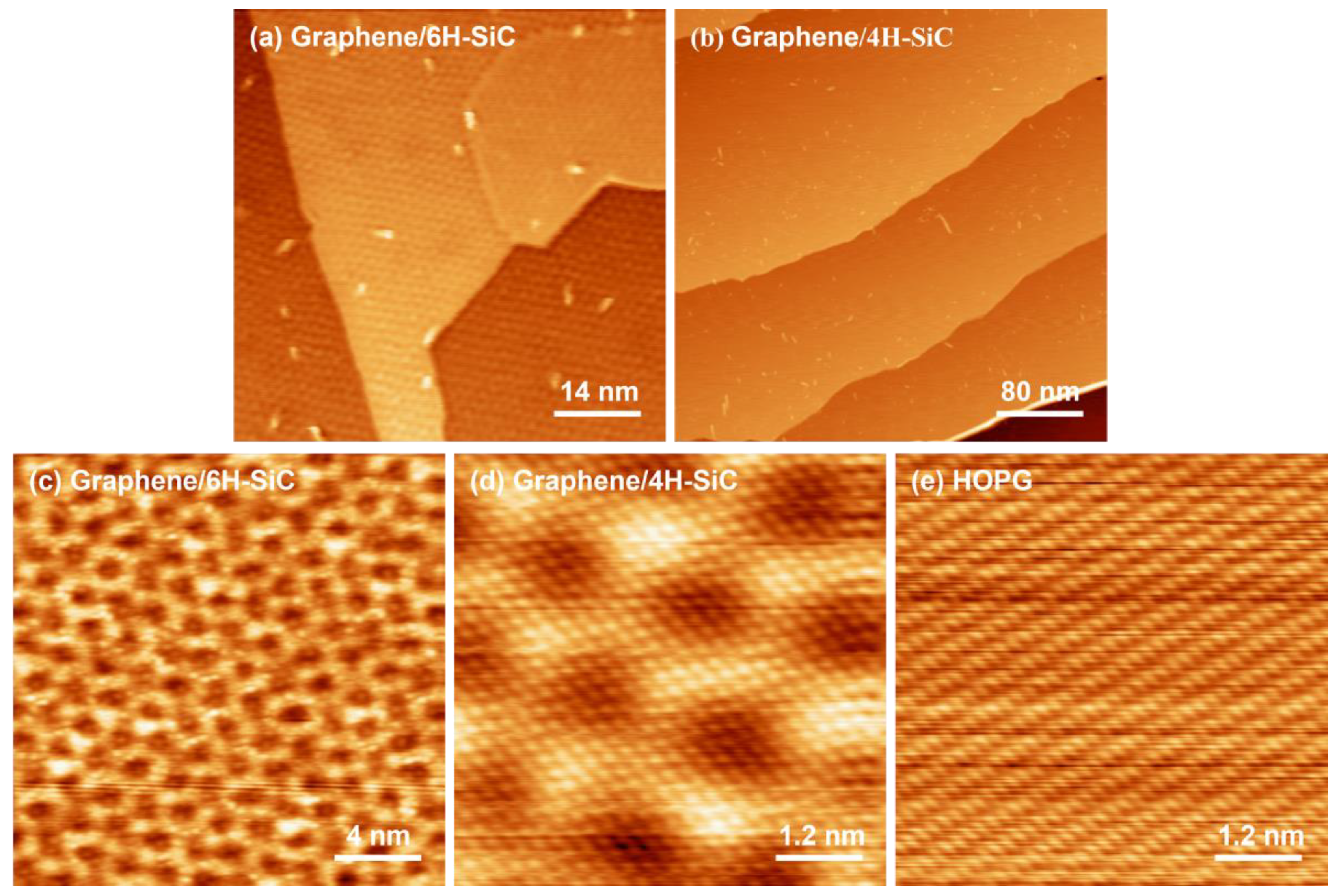
The samples are characterized by STM technique, as shown in Figure 3. The step edges can explicitly be observed. We prepared three groups of samples, including, single-layer graphene on 6H-SiC (Figure 3a), few-layer graphene on 4H-SiC (Figure 3b) and HOPG. Graphene with different layers shows different morphology. From Figure 3c, the hexagonal honeycomb lattice can be clearly observed. From Figure 3d, the moiré pattern can be observed in few-layer graphene. HOPG STM images are shown in Figure 3e, showing the atomic resolution of HOPG consisting of thick layers of graphene.
3.2. Thickness Characterization by SR-XPS
As discussed above, it is essential to estimate thickness precisely. In our experiment, we measure the C 1s spectrum by SR-XPS to gain information on the chemically different C atoms within the sample. For our thickness estimation method (introduced in the Method section), we are more interested in the peak intensity of graphene and SiC substrate.
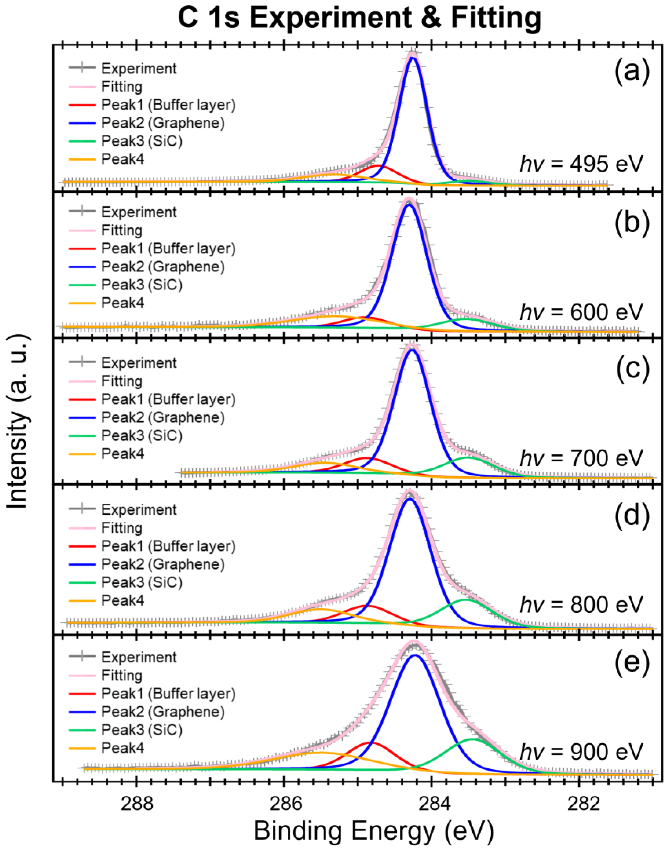
During the investigation, different photon energies are applied so that we can acquire the information of different “probe depth”. Figure 4 shows the experimental results of C 1s of few-layer graphene on SiC, measured with five different photon energies (495 eV, 600 eV, 700 eV, 800 eV and 900 eV). Different photon energy will also result in different inelastic mean free path. The inelastic mean free path of SiC and graphene (λSiC and λG, respectively) with different photon energies are shown in Table 1. In the energy range we used, smaller λ corresponds to smaller photon energy used.
In general, a smaller λ means we are effectuating a more surface-sensitive measurement. Since the graphene is on top of the SiC, we should acquire a more significant intensity of the graphene component with a smaller λG (smaller hv), and vice-versa. On the other hand, since SiC is at the bottom, we, therefore, need larger λSiC (higher hv) to acquire more SiC signals, i.e., larger λSiC (higher hv) will result in higher SiC intensity.
In Figure 4, it is clear that the green component is increasing with increasing photon energy (hv). Therefore, the green component is assigned to SiC. On the other hand, The main component (blue) can be easily assigned to graphene due to the decreasing ratio while increasing photon energy (hv). Next, we have the SiC component (green) behave similar to the graphene component (blue). We finally add another peak to present the other factors. The peak assignment is in accord with the previous studies [33,34,35,36]. We then use these four components, labeled as peak1 (buffer layer), peak2 (graphene), peak3 (SiC), and peak4 (other), to fit the C 1s curves.

Table 1.
Thickness estimation with the fitting result from Figure 4.
Table 1.
Thickness estimation with the fitting result from Figure 4.
| hv (eV) | hv (eV, Calibrated) | EK (eV) | λSiC [37] | λG [37] | IG/ISiC | d(Å) |
|---|---|---|---|---|---|---|
| (a) 495 * | 488.52 | 204.36 | 7.71 | 9.15 | 20.50 | 19.73 * |
| (b) 600 | 593.2 | 308.91 | 9.83 | 11.61 | 7.15 | 15.12 |
| (c) 700 | 691.39 | 407.12 | 11.78 | 13.89 | 5.10 | 14.85 |
| (d) 800 | 789.94 | 505.96 | 13.69 | 16.13 | 4.06 | 14.92 |
| (e) 900 | 888.71 | 604.47 | 15.55 | 18.32 | 3.45 | 15.22 |
* As detailed in the text, the estimated thickness deviates significantly from the reasonable value due to the small IMFP (λSiC, λG) of the used photon energy (495 eV).
In the following analysis, we will mainly make use of the fitting result of peak1, peak2, and peak3, which are assigned to the graphene layers (peak1 and peak2) and the SiC bulk (peak3), respectively [33,34]. The broad and weak peak4 is less interested [35].
With the attenuation method, we can acquire different intensity ratios regarding the surface and bulk and therefore acquire the information of the sample thickness. Most of the electrons are coming from the graphene so the intensity of peak2 is apparently more significant than the other lines. With the increasing photon energy, the excited electrons from the buffer layer can pass through graphene to the detector. As a result, peak1 becomes more evident, and its ratio to the total intensity increases. While the photon energy increases further, with the increasing λSiC, more electrons from the SiC substrate can escape from the sample. Therefore, the intensity of SiC substrate (peak3) increases with the increasing photon energy.
For the fitting procedure, we put 600 eV case as an example. We used four peaks for the fitting, including peak1 representing the interfacial buffer layer, peak2 from graphene, and peak3 originating from the SiC substrate. Next, we fix the position of peak1, peak2 and peak3 with a small error bar (peak position = 284.85 eV ± 0.05 eV, peak2 position = 284.25 eV ± 0.05 eV and peak3 position = 283.5 eV ± 0.05 eV) meanwhile their widths are set to about 0.75 eV, 0.65 eV and 0.85 eV, respectively. The initial setting keeps the fitting with reasonable physical meaning.
We used following formula to represent the ratio of C 1s line intensities of SiC substrate (ISiC) to graphene (IG) [33]:
where σ′ = dσ/dΩ stands for the differential cross-section of C 1s core level photoemission, T represents the transmission function of the analyzer, n is the density of carbon atoms, and λ indicates the inelastic mean free path. The subscript “G” and “SiC” indicate graphene layer and substrate, respectively. In the equation, “d” is the thickness of graphene we need. The C 1s cross-sections and are set to be equal. In addition, the transmission functions TG and TSiC are set to be equal for photo-electrons with close energies. The rate of can be recognized as a constant which is equal to 2.26 [33].
Finally, the thickness can be calculated by the following formula:
With the known constant according to the different photon energies, we can calculate the thickness of the graphene of the sample. The results are presented in Table 1.
In our work, the IG and ISiC in the formula are depending on the photon energy we use. We did not apply the normalization procedure. Instead, we directly use the ratio of the number of escaped electrons (intensity), as the ratio itself normalizes the other factors, such as the beam intensity (or beam current).
In fact, we not only conducted the experiments mentioned above from 495 eV to 900 eV, but also measured in the lower energy range, including 382 eV and 392 eV. Due to the surface sensitivity of such photon energy, the inelastic mean free path is too low (6.84 Å and 6.99 Å for 382 eV and 392 eV, respectively), such that most of the photo-electrons are coming from the top layer of graphene instead of the SiC substrate. From the peak fitting point of view, it is hard to add a peak of SiC peak at such low energy, making it difficult to properly estimate the adsorbate thickness.
We note that in Table 1 (marked with *), when the energy is 495 eV, the inelastic mean free path is much lower than the estimated thickness of the few-layer graphene (λG = 9.15 Å [37] < 15 Å of the graphene). This resulted in a significant error compared to the other results measured in higher energies. As a result, the calculated thickness measured with 495 eV photon energy is 19.73 Å, which is 4.7 Å large than the estimated result (15 Å). We believe this error is due to the low information depth with such photon energy (i.e., surface sensitivity). On the other hand, for the other higher energies (600 eV to 900 eV), where the inelastic mean free path becomes reasonably longer (11.61 Å to 18.32 Å) while keeping the surface sensitivity, the estimated thickness of the few-layer graphene is more reliable and in accord with the STM results. The overall error bar (600–900 eV) is less than 0.4 Å, showing an excellent accuracy of this method in estimating the few-layer graphene thickness.
4. Conclusions
In this work, we show a method to prepare pre-defined, few-layer graphene on 4H-SiC substrate that is epitaxially grown by the thermal decomposition of SiC. The sample is characterized by STM technique with atomic resolution, showing the high quality of the sample preparation by such a method. We introduce the improved attenuation method by changing the photon energy using the SR-XPS technique at the synchrotron facility. By calculating the intensity ratio of electrons from different components, the result shows that the few-layer graphene has a defined thickness of about 15 Å. The thickness estimation method is proved to be accurate without sample damage.
In the application of 2D materials, graphene, a vdW substrate, usually serves as an essential substrate due to its brilliant performance. It is of great significance to precisely control the thickness of the graphene substrate with a standard procedure. The non-damageable universal thickness characterization method is also essential to the 2D material application. We will develop the fabrication and characterization methods in the study for the broad 2D materials family in the future. We believe the fabrication method in the study can provide a suitable few-layer 2D substrate for future research on 2D electronics.
Author Contributions
Conceptualization, T.Z. and Y.W.; methodology, T.W., T.Z., K.N., C.L. and J.W.; SR-XPS experiment T.Z., L.J., Q.Z. and Z.X.; sample preparation, Z.H., P.Y., L.L.; STM characterizations, B.H., X.S., H.Y. and L.L.; writing, T.W. and T.Z. All authors have read and agreed to the published version of the manuscript.
Funding
This research was funded by the National Natural Science Foundation of China (Nos. 61901038, 62271048, 61971035).
Data Availability Statement
Data available on request from the corresponding author.
Acknowledgments
The authors acknowledge the staff of MIIT Key Laboratory for Low-Dimensional Quantum Structure and Devices, Beijing Institute of Technology, for the help of the sample preparation and characterization. We thank the staff of 4B9B-Photoemission Spectroscopy beamline at the Beijing Synchrotron Radiation Facility for all the help provided during the beamtimes. T.Z. is grateful for the support from the Beijing Institute of Technology Research Fund Program for Young Scholars.
Conflicts of Interest
The authors declare no conflict of interest.
References
- Novoselov, K.S.; Geim, A.K.; Morozov, S.V.; Jiang, D.; Zhang, Y.; Dubonos, S.V.; Grigorieva, I.V.; Firsov, A.A. Electric Field Effect in Atomically Thin Carbon Films. Science 2004, 306, 666–669. [Google Scholar] [CrossRef] [Green Version]
- Cao, Y.; Fatemi, V.; Demir, A.; Fang, S.; Tomarken, S.L.; Luo, J.Y.; Sanchez-Yamagishi, J.D.; Watanabe, K.; Taniguchi, T.; Kaxiras, E.; et al. Correlated insulator behaviour at half-filling in magic-angle graphene superlattices. Nature 2018, 556, 80–84. [Google Scholar] [CrossRef] [PubMed] [Green Version]
- Yu, K.; Van Luan, N.; Kim, T.; Jeon, J.; Kim, J.; Moon, P.; Lee, Y.H.; Choi, E.J. Gate tunable optical absorption and band structure of twisted bilayer graphene. Phys. Rev. B 2019, 99, 241405. [Google Scholar] [CrossRef] [Green Version]
- Moon, P.; Son, Y.W.; Koshino, M. Optical absorption of twisted bilayer graphene with interlayer potential asymmetry. Phys. Rev. B 2014, 90, 155427. [Google Scholar] [CrossRef] [Green Version]
- Novoselov, K.S.; Geim, A.K.; Morozov, S.V.; Jiang, D.; Katsnelson, M.I.; Grigorieva, I.; Dubonos, S.V.; Firsov, A.A. Two-dimensional gas of massless Dirac fermions in graphene. Nature 2005, 438, 197–200. [Google Scholar] [CrossRef] [Green Version]
- Nair, R.R.; Blake, P.; Grigorenko, A.N.; Novoselov, K.S.; Booth, T.J.; Stauber, T.; Peres, N.M.R.; Geim, A.K. Fine structure constant defines visual transparency of graphene. Science 2008, 320, 1308. [Google Scholar] [CrossRef] [Green Version]
- Lee, C.; Wei, X.; Kysar, J.W.; Hone, J. Measurement of the elastic properties and intrinsic strength of monolayer graphene. Science 2008, 321, 385–388. [Google Scholar] [CrossRef]
- Ganz, E.; Sattler, K.; Clarke, J. Scanning tunneling microscopy of the local atomic structure of two-dimensional gold and silver islands on graphite. Phys. Rev. Lett. 1988, 60, 1856. [Google Scholar] [CrossRef]
- Castellanos-Gomez, A.; Poot, M.; Steele, G.A.; Van Der Zant, H.S.; Agraït, N.; Rubio-Bollinger, G. Elastic properties of freely suspended MoS2 nanosheets. Adv. Mater. 2012, 24, 772–775. [Google Scholar] [CrossRef] [PubMed] [Green Version]
- Coleman, J.N.; Lotya, M.; O’Neill, A.; Bergin, S.D.; King, P.J.; Khan, U.; Young, K.; Gaucher, A.; De, S.; Smith, R.J.; et al. Two-dimensional nanosheets produced by liquid exfoliation of layered materials. Science 2011, 331, 568–571. [Google Scholar] [CrossRef]
- Ruoff, R. Calling all chemists. Nat. Nanotechnol. 2008, 3, 10–11. [Google Scholar] [CrossRef] [PubMed]
- Hanlon, D.; Backes, C.; Doherty, E.; Cucinotta, C.; Berner, N.C.; Boland, C.S.; Lee, K.; Harvey, A.; Lynch, P.; Gholamvand, Z.; et al. Liquid exfoliation of solvent-stabilized few-layer black phosphorus for applications beyond electronics. Nat. Commun. 2015, 6, 1–11. [Google Scholar] [CrossRef] [PubMed] [Green Version]
- Lin, L.; Deng, B.; Sun, J.; Peng, H.; Liu, Z. Bridging the gap between reality and ideal in chemical vapor deposition growth of graphene. Chem. Rev. 2018, 118, 9281–9343. [Google Scholar] [CrossRef] [PubMed]
- Li, X.; Cai, W.; An, J.; Kim, S.; Nah, J.; Yang, D.; Piner, R.; Velamakanni, A.; Jung, I.; Tutuc, E.; et al. Large-area synthesis of high-quality and uniform graphene films on copper foils. Science 2009, 324, 1312–1314. [Google Scholar] [CrossRef] [Green Version]
- Bradley, A.J.; Ugeda, M.M.; da Jornada, F.H.; Qiu, D.Y.; Ruan, W.; Zhang, Y.; Wickenburg, S.; Riss, A.; Lu, J.; Mo, S.-K.; et al. Probing the role of interlayer coupling and coulomb interactions on electronic structure in few-layer MoSe2 nanostructures. Nano Lett. 2015, 15, 2594–2599. [Google Scholar] [CrossRef]
- Liu, H.; Jiao, L.; Yang, F.; Cai, Y.; Wu, X.; Ho, W.; Gao, C.; Jia, J.; Wang, N.; Fan, H.; et al. Dense network of one-dimensional midgap metallic modes in monolayer MoSe2 and their spatial undulations. Phys. Rev. Lett. 2014, 113, 066105. [Google Scholar] [CrossRef] [Green Version]
- Liu, H.; Zheng, H.; Yang, F.; Jiao, L.; Chen, J.; Ho, W.; Gao, C.; Jia, J.; Xie, M. Line and point defects in MoSe2 bilayer studied by scanning tunneling microscopy and spectroscopy. ACS Nano 2015, 9, 6619–6625. [Google Scholar] [CrossRef] [Green Version]
- Virojanadara, C.; Syväjarvi, M.; Yakimova, R.; Johansson, L.I.; Zakharov, A.A.; Balasubramanian, T. Homogeneous large-area graphene layer growth on 6H-SiC (0001). Phys. Rev. B 2008, 78, 245403. [Google Scholar] [CrossRef]
- Nagashio, K.; Nishimura, T.; Kita, K.; Toriumi, A. Mobility variations in mono-and multi-layer graphene films. Appl. Phys. Express 2009, 2, 025003. [Google Scholar] [CrossRef] [Green Version]
- Zhang, Y.Y.; Gu, Y.T. Mechanical properties of graphene: Effects of layer number, temperature and isotope. Comput. Mater. Sci. 2013, 71, 197–200. [Google Scholar] [CrossRef]
- Park, H.J.; Meyer, J.; Roth, S.; Skákalová, V. Growth and properties of few-layer graphene prepared by chemical vapor deposition. Carbon 2010, 48, 1088–1094. [Google Scholar] [CrossRef] [Green Version]
- Novoselov, K.S.; Fal′ko, V.I.; Colombo, L.; Gellert, P.R.; Schwab, M.G.; Kim, K. A roadmap for graphene. Nature 2012, 490, 192–200. [Google Scholar] [CrossRef] [PubMed]
- Nilsson, J.; Neto, A.H.C.; Guinea, F.; Peres, N.M.R. Electronic properties of graphene multilayers. Phys. Rev. Lett. 2006, 97, 266801. [Google Scholar] [CrossRef] [Green Version]
- Casiraghi, C.; Hartschuh, A.; Lidorikis, E.; Qian, H.; Harutyunyan, H.; Gokus, T.; Novoselov, K.; Ferrari, A.C. Rayleigh imaging of graphene and graphene layers. Nano Lett. 2007, 7, 2711–2717. [Google Scholar] [CrossRef] [Green Version]
- Ferrari, A.C.; Basko, D.M. Raman spectroscopy as a versatile tool for studying the properties of graphene. Nat. Nanotechnol. 2013, 8, 235–246. [Google Scholar] [CrossRef] [PubMed] [Green Version]
- Shearer, C.J.; Slattery, A.D.; Stapleton, A.J.; Shapter, J.; Gibson, C.T. Accurate thickness measurement of graphene. Nanotechnology 2016, 27, 125704. [Google Scholar] [CrossRef] [PubMed]
- Norimatsu, W.; Kusunoki, M. Transitional structures of the interface between graphene and 6H–SiC (0001). Chem. Phys. Lett. 2009, 468, 52–56. [Google Scholar] [CrossRef]
- Mishra, N.; Boeckl, J.; Motta, N.; Iacopi, F. Graphene growth on silicon carbide: A review. Phys. Status Solidi A 2016, 213, 2277–2289. [Google Scholar] [CrossRef]
- Salapaka, S.M.; Salapaka, M.V. Scanning probe microscopy. IEEE Control Syst. Mag. 2008, 28, 65–83. [Google Scholar]
- Powell, C.J.; Jablonski, A. Evaluation of calculated and measured electron inelastic mean free paths near solid surfaces. J. Phys. Chem. Ref. Data 1999, 28, 19–62. [Google Scholar] [CrossRef]
- Graber, T.; Forster, F.; Schöll, A.; Reinert, F. Experimental determination of the attenuation length of electrons in organic molecular solids: The example of PTCDA. Surf. Sci. 2011, 605, 878–882. [Google Scholar] [CrossRef]
- Zhang, T.; Grazioli, C.; Guarnaccio, A.; Brumboiu, I.E.; Lanzilotto, V.; Johansson, F.O.L.; Beranová, K.; Coreno, M.; de Simone, M.; Brena, B.; et al. m-MTDATA on Au (111): Spectroscopic Evidence of Molecule–Substrate Interactions. J. Phys. Chem., C 2022, 126, 3202–3210. [Google Scholar] [CrossRef]
- Mikoushkin, V.M.; Shnitov, V.V.; Lebedev, A.A.; Lebedev, S.P.; Nikonov, S.Y.; Vilkov, O.Y.; Iakimov, T.; Yakimova, R. Size confinement effect in graphene grown on 6H-SiC (0001) substrate. Carbon 2015, 86, 139–145. [Google Scholar] [CrossRef] [Green Version]
- Rollings, E.; Gweon, G.-H.; Zhou, S.Y.; Mun, B.S.; McChesney, J.L.; Hussain, B.S.; Fedorov, A.V.; First, P.N.; de Heer, W.A.; Lanzara, A. Synthesis and characterization of atomically thin graphite films on a silicon carbide substrate. J. Phys. Chem. Solids 2006, 67, 2172–2177. [Google Scholar] [CrossRef] [Green Version]
- Soe, W.H.; Rieder, K.H.; Shikin, A.M.; Mozhaiskii, V.; Varykhalov, A.; Rader, O. Surface phonon and valence band dispersions in graphite overlayers formed by solid-state graphitization of 6H−SiC (0001). Phys. Rev. B 2004, 70, 115421. [Google Scholar] [CrossRef]
- Johansson, L.I.; Owman, F.; Mårtensson, P. High-resolution core-level study of 6H-SiC (0001). Phys. Rev. B 1996, 53, 13793. [Google Scholar] [CrossRef] [PubMed]
- Tanuma, S.; Powell, C.J.; Penn, D.R. Calculation of electron inelastic mean free paths (IMFPs) VII. Reliability of the TPP-2M IMFP predictive equatio. Surf. Interf. Anal. 2003, 3, 268–275. [Google Scholar] [CrossRef]
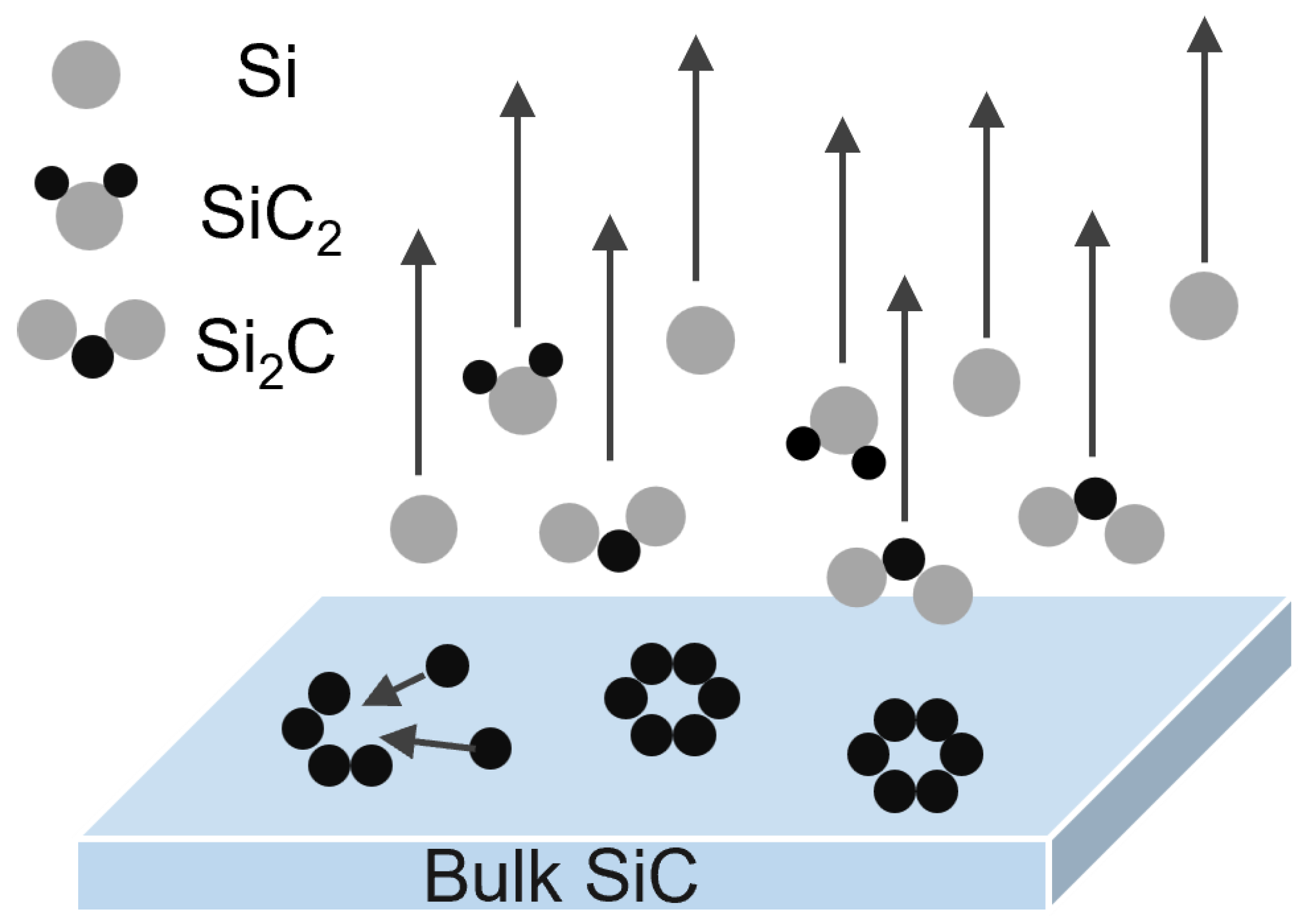
Figure 1.
Graphene formation on SiC. During the thermal decomposition process, Si atoms and particles containing Si atom escape from the SiC substrate surface. Residual C atoms on the substrate surface tend to form a honeycomb lattice. Blue-grey bulk is SiC substrate. The Grey and black solid circles are Si atoms and C atoms, respectively.

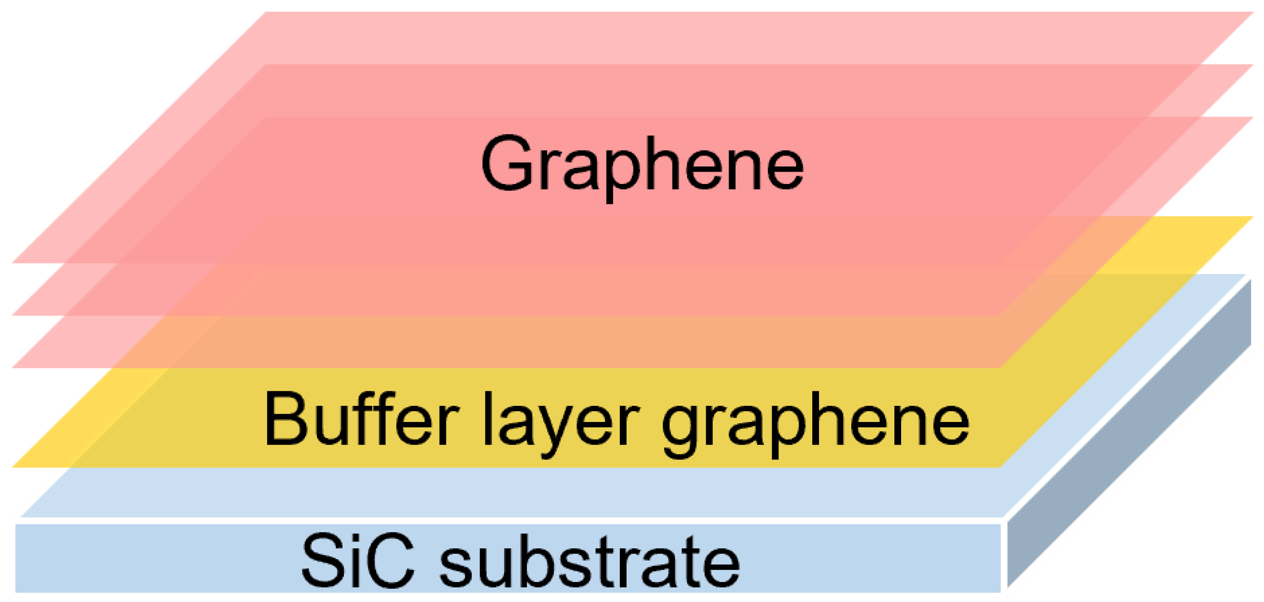
Figure 2.
The schematic representation of the structure of the few-layered graphene sample. In between the few-layered graphene and the SiC substrate, there is the so-called “buffer layer” which is covalently bonded to SiC and has weak force to the top graphene layer by the vdWs force.
Figure 2.
The schematic representation of the structure of the few-layered graphene sample. In between the few-layered graphene and the SiC substrate, there is the so-called “buffer layer” which is covalently bonded to SiC and has weak force to the top graphene layer by the vdWs force.

Figure 3.
STM images. (a,b) Large-scale scan of graphene with different thickness grown on SiC substrate. (a) STM image of single-layer graphene on 6H-SiC (Vs = −0.9 V, It = 200 pA). (b) STM image of few-layer graphene on 4H-SiC, with the fabrication method introduced in the study (Vs = −1.5 V, It = 10 pA). (c–e) Atomic resolution images of graphene with different layers. (c) Zoom-in STM image of (a), single-layer graphene/6H-SiC (Vs = −1.3 V, It = 500 pA). (d) Zoom-in STM image of (b), few-layer graphene on 4H-SiC (Vs = −80 mV, It = 5 nA). (e) Zoom-in STM image of HOPG (Vs = 170 mV, It = 1.5 nA).

Figure 4.
C 1s XPS results of few-layer graphene sample measured by different photon energy: (a) 495 eV, (b) 600 eV, (c) 700 eV, (d) 800 eV and (e) 900 eV, respectively. As shown in the figure, the peak intensity is depending on the different photon energy used. We use this result to estimate the thickness, which is shown in Table 1. The resolution depends on the photon energy used but is always better than 600 meV. Grey and pink lines are experiment and fitting results, respectively. The red, blue and green peaks represent the signals coming from the buffer layer, graphene and SiC substrate, respectively.

Disclaimer/Publisher’s Note: The statements, opinions and data contained in all publications are solely those of the individual author(s) and contributor(s) and not of MDPI and/or the editor(s). MDPI and/or the editor(s) disclaim responsibility for any injury to people or property resulting from any ideas, methods, instructions or products referred to in the content. |
© 2022 by the authors. Licensee MDPI, Basel, Switzerland. This article is an open access article distributed under the terms and conditions of the Creative Commons Attribution (CC BY) license (https://creativecommons.org/licenses/by/4.0/).
Share and Cite
MDPI and ACS Style
Wang, T.; Jia, L.; Zhang, Q.; Xu, Z.; Huang, Z.; Yuan, P.; Hou, B.; Song, X.; Nie, K.; Liu, C.; et al. Fabrication and Characterization of Pre-Defined Few-Layer Graphene. Physchem 2023, 3, 13-21. https://doi.org/10.3390/physchem3010002
AMA Style
Wang T, Jia L, Zhang Q, Xu Z, Huang Z, Yuan P, Hou B, Song X, Nie K, Liu C, et al. Fabrication and Characterization of Pre-Defined Few-Layer Graphene. Physchem. 2023; 3(1):13-21. https://doi.org/10.3390/physchem3010002
Chicago/Turabian StyleWang, Tingting, Liangguang Jia, Quanzhen Zhang, Ziqiang Xu, Zeping Huang, Peiwen Yuan, Baofei Hou, Xuan Song, Kaiqi Nie, Chen Liu, and et al. 2023. "Fabrication and Characterization of Pre-Defined Few-Layer Graphene" Physchem 3, no. 1: 13-21. https://doi.org/10.3390/physchem3010002