
Hybrid Superconducting/Magnetic Multifunctional Devices in Two-Dimensional Systems


1
Materials Science and Engineering Department, Guangdong Technion Israel Institute of Technology, Shantou 515063, China
2
Zhejiang Beyondsun Green Energy Technology Co., Ltd., No.888. Zhili Section of G318, Zhili Town, Huzhou 313008, China
Physchem 2022, 2(4), 347-356; https://doi.org/10.3390/physchem2040025
Submission received: 11 October 2022
/
Revised: 20 November 2022
/
Accepted: 22 November 2022
/
Published: 25 November 2022
Abstract
:The emergence of unexpected properties in two-dimensional materials, interfaces, and nanostructured materials opens an exciting framework for exploring new devices and applications. Recent advances in materials design and the nano structurization of novel, low-dimensional materials, surfaces, and interfaces offer a novel playground to design efficient multifunctional materials-based devices. Low-dimensional materials exhibit peculiarities in their electronic, magnetic, and optical properties, changing with respect to the bulk when they are layered down to a single layer, in addition to their high tunability. Their crystal structure and chemical bonds lead to inherent unique mechanical properties. The fabrication of van der Waals heterostructures by stacking materials with different properties, the better control of interfaces, and the tunability of the physical properties by mechanical strain, and chemical and electronic doping allow for the exploration of multifunctional devices with superconducting, magnetic, and optical properties and unprecedented degrees of freedom in terms of fabrication and tunability.
1. Introduction
The possibility of fabricating devices with highly controllable accuracy at nanoscales is essential for manipulating and tailoring the physical and electronic properties of multifunctional devices. The materials’ electronic properties exhibit novel features when their sizes are scaled down to the two-dimensional limit, or comparable features to the characteristic lengths determining their physical properties, similar to the case of superconducting and magnetic materials [1,2].
The isolation and re-discovery of graphene by Novoselov and Geim in 2004 [3] and the following emergence of other two-dimensional (2D) materials [4,5] paved the way to design devices based on van der Waals heterostructures [6] at will with semiconducting, insulating, magnetic, and/or superconducting properties with an unprecedented degree of freedom [7]. Such freedom in designing and fabricating heterostructures of materials with different properties opens a framework for investigating the interactions of the fundamental properties and functionalities at the nanoscale. Moreover, when the thickness is reduced to a single atomic layer, 2D materials exhibit properties that differ from those in bulk or with a higher number of layers. This is the case of MoS2, which becomes a direct bandgap semiconductor when the thickness is reduced to one single mono-layer (ML) [8]. This change in the energy band structure and, therefore, in their optoelectronic properties represents a new scenario to explore new effects characterized by these one-layer particularities. Furthermore, superconductivity and magnetism, which are not only competitive effects, but are also combined in hybrid devices at the nanoscale, coexist under certain regimes, exhibiting interesting collaborative effects, which are still unexplored when assembled in 2D van der Waals heterostructures [9].
In hybrid superconducting–magnetic devices, two order parameters compete, with partial or total order suppressing [10]. On the other hand, low-dimensionality magnetic or/and superconducting materials, either obtained by nanofabrication techniques or as ultra-thin films at the two-dimensional (2D) limit, are an outbreak with new, emerging effects [11]. Such nanoscale hybrid devices have shown unique competitive and collaborative features between superconductivity and magnetism. The presence of periodical arrays of nanomagnetic features leads to commensurability effects between the superconducting vortex lattice and the magnetic array. These commensurability effects occur when the periodicities and sizes of the nanomagnetic features are of the order of the superconducting coherence length and Abrikosov lattice parameter [12,13] Superconductivity and magnetism are, in general, antagonistic phenomena, but the interplay between them, depending on the different structural parameters of the superconducting/magnetic materials and the oscillating behavior of the superconducting order parameter within the magnetic layers, allows for novel effects under these two competing orders [14]. Among them, new developments in cryogenic memories exploit the superconducting and magnetic properties, similar to the case of a two-layer magnetic spin valve integrated within a Josephson junction [15,16,17,18]. The exchange field suppression of the superconducting order parameter is a tunable and switchable behavior scalable to the dimensions of nanometer devices. With thin enough superconducting spacing layers, the superconductivity can be controlled by the magnetic order of the ferromagnetic layers [19]. The superconducting proximity effect leads to the leakage of superconducting correlations in magnetic proximity layers and the superconducting transition temperature can be tuned as the Josephson current [20,21,22,23].
Apart from many of these well-known phenomena, there is continuous activity related to “unconventional” superconductivity mechanisms [24,25,26,27]. New materials and fabrication methods are providing better quality and controlled interfaces with two-dimensional characteristics, showing new emerging devices [24,25]. These led to an unexpected, or, at least, not fully understandable, picture of the superconductivity mechanism description in these devices in terms of conventional or unconventional superconductors. Additionally, the capability to manipulate the scalability of devices down to a pure 2D limit provides an interesting framework to explore superconductive phases in novel devices, even coexisting phases, like magic-angle graphene, which becomes a ferromagnet by inducing a spin-orbit coupling, both competing for superconductivity and magnetism when coexisting [28,29,30].
The motivation to search for high-temperature superconductors or superconducting qubits as building blocks of a quantum computer has resulted in continuous discoveries. Additionally, ultrathin materials may pave the way for personal-sized quantum devices using superconducting qubits as building blocks of a quantum computer, such as boron nitride (hBN) as a low-loss dielectric for superconducting quantum circuits and qubits [31].
This review is focused on the competing/collaborative effects that have emerged in devices with their dimensions scaled down to relevant characteristic lengths of superconducting and magnetic fundamental parameters. There are different approaches to tailoring the intrinsic properties of materials by nano-scaling devices. This review will be focused on the results obtained by nanolithography techniques to design an interacting potential landscape in materials (pinning). This approach can be implemented in many contexts to enhance the interaction between materials with different properties and with external fields or light [32,33,34]. In Section 1, devices fabricated by nanotechnological means exhibit commensurability effects between superconducting vortices and periodic arrays of nanomagnetic patterned features. This section highlights the importance of nanotechnology to fabricate such devices with controllable sizes comparable to the characteristic lengths of the fundamental inherent parameters of magnetism and superconductivity. This technique can also be combined in the fabrication of new heterostructures based on 2D materials. Section 2 reviews the appearance of new 2D magnetic and superconducting materials, the properties of which differ from their bulk counterparts and exhibit novel features only present in the 2D regime. The assembly of nanodevices and van der Waals heterostructures by the deterministic placement of 2D materials [7] makes the combination of these novel 2D materials with magnetic and superconducting properties in a new fashion, with high tunability by different means, feasible. This section also reviews the interfaces and superlattices of different materials with a large diversity of types, properties, and forms, where unique superconducting and magnetic phenomena arise from the two-dimensionality of the system.
- Superconducting/Hybrid Devices at the Nanoscale
Nanoscale devices produced by nanofabrication techniques open up scenarios in which materials’ properties can be tailored and tuned at will. Competitive/collaborative effects in superconductors and/or magnetic-based devices can be explored when their sizes are scaled down to their relevant characteristic lengths in a controlled and combined fashion.
In this way, superconducting properties, such as vortex lattice pinning and dynamics, related to the characteristic coherent lengths can be strongly modified by engineering hybrid devices, as has been shown during the last few decades [35,36]. By using arrays of magnetic nanofeatures with different sizes, shapes, geometries, and periodicities [14,37,38,39,40,41], effects, such as superconducting vortex pinning, induced channeling motion, and superconducting ratchet, have been reported for such hybrid samples [42,43,44].
By patterning arrays of periodic nanostructured features, a new landscape can be set in the material in which they are embedded to modify its transport properties, provided that the periodicities and sizes of the nanostructured features are comparable to the relevant dimensions that characterize the materials’ properties. By changing the sizes, shapes, periodicities, and types of materials from which the nanofeatures are produced, an underlying potential can be engineered to tailor the transport properties at will. Arrays of magnetic nanofeatures embedded in superconducting materials have shown how the transport and electrical properties of these devices can be tailored: low resistance results in low dissipative effects, and preferred directional motion with lower resistance or rectification effects can be realized, as shown in Figure 1. This is a clear example of how the inherent fundamental material properties can be tuned and modified by imprinting an underlying engineered template.
2. Magnetic and Superconducting Two-Dimensional Materials
2.1. Emerging Two-Dimensional Magnets
Research on 2D materials continues to grow interest in emerging phenomena and optoelectronic properties to be explored in this regime, different from their bulk or layered state. The isolation of 2D materials by mechanical exfoliation allows for achieving van der Waals (vdW) heterostructures with an unprecedented variety of possibilities in terms of the fabrication and combination of materials with any property, and the tunability of their properties as represented in Figure 2. Exfoliated materials with high crystallinity, few defects, and almost any electronic/magnetic/optical properties can be combined in the search for new collaborative effects in devices based on such heterostructures. Either by combining 2D materials layer by layer in heterostructures or by hybridizing and functionalizing other materials, new device concepts can be achieved. The demonstration of room-temperature ferromagnetism in an atomically thin layer broadens the prospects for device applications of 2D van der Waals materials [45,46,47]. The use of magnetic 2D materials as part of vdW heterostructures can increase the functionality of the heterostructures for different applications and, with proximity to other 2D crystals, modify the magnetic properties, enabling magnetic tunnel junctions to be obtained by sandwiching thin films of insulating or semiconductor materials (such as hBN or TMDC) between two layers of metallic ferromagnetic crystals with Fe3GeTe2 and spin-valves in Fe3GeTe2/hBN/Fe3GeTe2 junctions due to the different coercive fields of the top and bottom electrodes [48].
The magnetic order can be changed not only with temperature, but also when materials’ dimensions are reduced to the very limit of 2D. The magnetic states in 2D materials can differ from those in bulk crystals. Changes in the dimensionality of materials have evidenced such effects [1].
Two-dimensional materials practically cover the whole range of properties, from metals to semimetals, topological insulators, semiconductors, and insulators. Additionally, they exhibit correlation phenomena, such as superconductivity, charge density waves, and Mott insulators. The amazing properties exhibited by graphene as a zero-gap semiconductor [3], which completely differentiates it from semimetal graphite with a band overlap, are also present in many other monolayered materials. In the case of magnetic materials, such as ferromagnetic Cr2Ge2Te6, the Curie temperature is suppressed when changing from 3D to 2D and ferromagnetic order is present down to the bilayer system [49,50,51,52,53]. Additionally, monolayer materials, such as CrI3, show Ising-type order and magnetization stable up to 45K [45,54]. Monolayers and a few layers of NiPS3 [55], FePS3 [56,57,58], and CrSiTe3 [59] display magnetic order in the bulk form, and magnetism is still present in the 2D limit. Magnetism can be found in atomically thin monolayer CrI3 and bilayer CrGeTe3 [45,49].
In the case of anisotropic magnetic materials, either from an intrinsic strong spin–orbit coupling [60,61] from magneto-crystalline anisotropy or other extrinsic effects leading to magnetic anisotropy, magnetism can be stable in the monolayer limit with a different critical temperature to the bulk materials, similar to CrI3 and Fe3GeTe2. If, in addition to more exotic phenomena, a magnetic order persists above room temperature, it is similar to the ferromagnetic order in monolayers of VSe2 grown on either graphite or MoSe2 [51].
These recent discoveries of atomically thin magnetic crystals and 2D magnets have paved the way for achieving vdW heterostructures, in which not only novel magnetic effects are present, but also additional tunability associated with the inherent nature of 2D materials, including their mechanical properties and simple integration of multi-layered heterostructures [62]. Among all of the possible tuning mechanisms in this material, the electrostatic control of magnetism in gated structures is of great interest for device applications [63]. Gating can change the critical temperature and the coercive field, with the possibility of altering electrostatically the magnetic properties of systems in which the magnetization and the electrical polarization are intrinsically coupled [64,65]. The applied electric field changes the magnetization by the magnetoelectric effect.
By combining them, unique vdW heterostructures and devices can be obtained with new physical effects [66].
2.2. Two-Dimensional Superconductors and Interfaces
Ultrathin 2D superconductors have undergone remarkable progress, mostly driven by rapid advancements in nanotechnology in recent years. Two-dimensional superconductors at the strict realization of the two-dimensional limit, with single-atomic-layer materials, have also opened up interest in a new framework for studying superconductivity phenomena at the 2D limit and the production of pure/hybrid superconducting devices [67,68,69]. Again, the unique features of 2D superconductors can help to understand how new physics and novel phenomena emerge because of the atomic-scale thicknesses of the materials. These systems represent a new scenario where the layered structure and highly crystalline properties of 2D superconductors can be further analyzed. The isolation of atomic layers by the exfoliation of layered materials, following graphene, has motivated the research into monolayered superconductors and those with a few layers [70,71]. The discovery of superconductivity in magic-angle twisted bilayer graphene and transition-metal dichalcogenide monolayers has boosted the interest in 2D superconductors and 2D superconducting devices [27,72,73].
Initially, the possibility of inducing superconductivity in graphene by the proximity effect [74] raised interest in not only adding superconductive properties to graphene, but also producing hybrid superconducting heterostructures with graphene. Later, the demonstration of robust superconductivity at the ML limit has expanded the family of 2D superconducting materials. Superconductivity has been observed in ultrathin metal films down to a few layers [75,76], and also in single layers of ordered metal atoms, which represents the ultimate 2D limit of a crystalline film, such as single atomic layers of Pb and In grown epitaxially on Si(111) substrates [24]. Superconductivity has also been demonstrated in atomically thin exfoliated 2D materials with a layer number dependence of superconductivity, similar to the case of NbSe2 and other 2D transition metal dichalcogenides with samples down to monolayer thickness.
Remarkable achievements with 2D superconductors have been observed, such as the strong enhancement of Tc up to 40–100 K in one-unit-cell-thick FeSe layers epitaxially grown on SrTiO3 substrates to the critical temperature of 8 K in bulk FeSe [26]. Such behavior opens the possibility for investigating the realization of high-Tc superconductors based on atomic-scale layers strongly interacting with the substrate, and the role played by the interface and accumulated or transferred charge. Additionally, the reduction of the thickness to the atomic scale 2D limit reveals robust superconductivity at low temperatures, providing a high-quality structure and composition. This ensures the potential for real applications based on 2D material devices. The enhanced superconductivity mechanism is still under discussion, but it suggests that the strengthened Cooper pairing in one-unit-cell FeSe/STO originates from the interface effects, specifically the charge transfer and coupling to phonon modes in the TiO2 plane. Understanding the mechanism underlying the high-temperature superconductivity in this 2D limit between single-atomic-layer superconductors and their interfaces with substrates provides a new perspective for the exploration of new superconductors by interface engineering.
Two-dimensional superconductors with atomic-scale thickness cover a wide spectrum, which includes metal ultrathin films and atomic layers on semiconductor surfaces, graphene and atomic sheets of many layered materials, iron selenide on oxide substrates, and organic conductors on metal surfaces. The relevance of the interface effects represents an attractive potentiality in the investigation of interfaces and superlattices of heterostructures composed of cuprates, perovskite oxides, and rare-earth-metal heavy-fermion compounds, interfaces of electric double-layer transistors, etc.
Clean interfaces of two spatially separated quantum states enable unique current transport phenomena, such as the resonant tunneling of charge carriers, provided that carrier scattering related to interfacial imperfections can be suppressed. Heterostructures of MoS2–WSe2–graphene, Wse2–MoS2–graphene in an atomically thin stack, and van der Waals double-quantum wells based on WSe2 with a few layers [77] have shown resonant tunneling with room temperature negative-differential-resistance characteristics [78] This is a key feature of novel nano-electronic circuits that utilize bistability and positive feedback.
The integration of 2D van der Waals materials with high control of the interfacial imperfections can lead to novel electronic and optical properties not found in the constituent layers. Additionally, 2D materials exhibit inherent peculiarities that allow for their electronic properties to be tuned in a controllable fashion. Their electronic properties can be tuned by gate fields, doping, or intercalation (Iontronics) [79]. La2−xSrxCuO4, a representative cuprate high-Tc superconductor, which also shows superconductivity at one-unit-cell thickness, was electrically tuned to an insulating state, revealing an S–I transition driven by quantum-phase fluctuations [80,81]. Recent technological breakthroughs in field-effect transistors (FET) using an electric-double-layer (EDL) gate have enabled carrier doping with an unprecedentedly high level (n2D∼1014 cm−2) at the subsurface region, leading to the successful production of field-induced 2D superconductivity in various insulating materials, including SrTiO3 and ZrNCl [82,83,84].
The electronic properties can be tuned in Moiré heterostructures by twisting the relative orientation between layers or stacks (Twistronics) [85], leading to the onset of superconductivity in magic-angle graphene bilayers [27].
All of this progress in 2D superconductors has led to the realization of superconducting/graphene hybrid devices, such as tunable Josephson junctions, magnetic Josephson junctions, and superconducting diodes and SQUIDs [67], which represent an important step forward in superconducting electronics [86,87,88,89].
3. Conclusions
We are at the beginning of an exciting framework for the production of van der Waals heterostructures demonstrating extraordinary and outstanding capabilities by assembling MLs with unique electronic properties.
Structures formed by ferromagnetic and superconducting layers allow for the fundamental understanding of the competition between superconducting and magnetic ordering, as well as new device functionalities [90,91]
The tunability of the superconductive properties by controlling the magnetization of the FM layers allows for controlling the magnetic properties through the superconductivity.
Additionally, a spin-valve based on hybrid ferromagnetic insulator/superconducting tunnel structures can be produced by the proximity effect [92] between ferromagnetic and superconducting materials: a superconductor with a spin-split excitation spectrum behaves as an ideal ferromagnetic spin-injector in a tunneling junction [93,94]. The combination of two such spin-split superconductors with independently tunable magnetizations may be used as an ideal absolute spin valve [95]. By applying an external magnetic field, or by the proximity of a magnetic insulator, the superconducting film shows a spin-splitting for the realization of applications [96], such as logical elements in cryogenics superconductor-based computers and superconducting spintronics with a highly polarized spin current source as a spintronic building block to implement low-dissipation cryogenic non-volatile memories [97,98].
The competition and coexistence of superconductivity with other many-body electronic states, such as magnetism and CDW, also enrich the physics and phenomena found in the regime of the 2D limit, enriching the framework of hybrid device-based devices and applications.
Funding
This research received no external funding.
Institutional Review Board Statement
Not applicable.
Informed Consent Statement
Not applicable.
Acknowledgments
This work was supported by the innovation team project of Zhejiang Province (2019R01012).
Conflicts of Interest
The author declares no conflict of interest.
References
- Fernández-Pacheco, A.; Streubel, R.; Fruchart, O.; Hertel, R.; Fischer, P.; Cowburn, R.P. Three-dimensional nanomagnetism. Nat. Commun. 2017, 8, 15756. [Google Scholar] [CrossRef] [Green Version]
- Haviland, D.B.; Liu, Y.; Goldman, A.M. Onset of superconductivity in the two-dimensional limit. Phys. Rev. Lett. 1989, 62, 2180. [Google Scholar] [CrossRef]
- Novoselov, K.S.; Geim, A.K.; Morozov, S.V.; Jiang, D.; Zhang, Y.; Dubonos, S.V.; Grigorieva, I.V.; Firsov, A.A. Electric field effect in atomically thin carbon films. Science 2004, 306, 666–669. [Google Scholar] [CrossRef] [Green Version]
- Xu, M.; Liang, T.; Shi, M.; Chen, H. Graphene-Like Two-Dimensional Materials. Chem. Rev. 2013, 113, 3766–3798. [Google Scholar] [CrossRef]
- Choi, W.; Choudhary, N.; Han, G.H.; Park, J.; Akinwande, D.; Lee, Y.H. Recent development of two-dimensional transition metal dichalcogenides and their applications. Mater. Today 2017, 20, 116–130. [Google Scholar] [CrossRef]
- Geim, A.; Grigorieva, I. Van der Waals heterostructures. Nature 2013, 499, 419–425. [Google Scholar] [CrossRef] [Green Version]
- Frisenda, R.; Navarro-Moratalla, E.; Gant, P.; De Lara, D.P.; Jarillo-Herrero, P.; Gorbachev, R.V.; Castellanos-Gomez, A. Recent progress in the assembly of nanodevices and van der Waals heterostructures by deterministic placement of 2D materials. Chem. Soc. Rev. 2017, 47, 53–68. [Google Scholar] [CrossRef] [Green Version]
- Mak, K.F.; Lee, C.; Hone, J.; Shan, J.; Heinz, T.F. Atomically Thin MoS2: A New Direct-Gap Semiconductor. Phys. Rev. Lett. 2010, 105, 136805. [Google Scholar] [CrossRef] [Green Version]
- Zhu, X.; Guo, Y.; Cheng, H.; Dai, J.; An, X.; Zhao, J.; Tian, K.; Wei, S.; Zeng, X.C.; Wu, C.; et al. Signature of coexistence of superconductivity and ferromagnetism in two-dimensional NbSe2 triggered by surface molecular adsorption. Nat. Commun. 2016, 7, 11210. [Google Scholar] [CrossRef] [PubMed] [Green Version]
- Buzdin, A.I. Proximity effects in superconductor-ferromagnet heterostructures. Rev. Mod. Phys. 2005, 77, 935–976. [Google Scholar] [CrossRef]
- Li, Y.; Yang, B.; Xu, S.; Huang, B.; Duan, W. Emergent Phenomena in Magnetic Two-Dimensional Materials and van der Waals Heterostructures. ACS Appl. Electron. Mater. 2022, 4, 3278–3302. [Google Scholar] [CrossRef]
- Baert, M.; Metlushko, V.V.; Jonckheere, R.; Moshchalkov, V.V.; Bruynseraede, Y. Composite Flux-Line Lattices Stabilized in Superconducting Films by a Regular Array of Artificial Defects. Phys. Rev. Lett. 1995, 74, 3269–3272. [Google Scholar] [CrossRef]
- Harada, K.; Kamimura, O.; Kasai, H.; Matsuda, T.; Tonomura, A.; Moshchalkov, V.V. Direct Observation of Vortex Dynamics in Superconducting Films with Regular Arrays of Defects. Science 1996, 274, 1167–1170. [Google Scholar] [CrossRef]
- Buzdin, A. Mixing superconductivity and magnetism. Nat. Mater. 2004, 3, 751–752. [Google Scholar] [CrossRef] [PubMed]
- Golovchanskiy, I.A.; Abramov, N.N.; Stolyarov, V.S.; Bolginov, V.V.; Ryazanov, V.V.; Golubov, A.A.; Ustinov, A. Ferromagnet/Superconductor Hybridization for Magnonic Applications. Adv. Funct. Mater. 2018, 28, 1802375. [Google Scholar] [CrossRef]
- Baek, B.; Rippard, W.H.; Benz, S.P.; Russek, S.E.; Dresselhaus, P.D. Hybrid superconducting-magnetic memory device using competing order parameters. Nat. Commun. 2014, 5, 3888. [Google Scholar] [CrossRef] [Green Version]
- De Simoni, G.; Strambini, E.; Moodera, J.S.; Bergeret, F.S.; Giazotto, F. Toward the Absolute Spin-Valve Effect in Superconducting Tunnel Junctions. Nano Lett. 2018, 18, 6369–6374. [Google Scholar] [CrossRef] [Green Version]
- Golubov, A.A.; Kupriyanov, M.Y. Controlling magnetism. Nat. Mater. 2017, 16, 156–157. [Google Scholar] [CrossRef]
- Alija, A.; Pérez de Lara, D.; Gonzalez, E.M.; Kakazei, G.N.; Sousa, J.B.; Araujo, J.P.; Hierro-Rodriguez, A.; Martín, J.I.; Alameda, J.M.; Vélez, M.; et al. Ferromagnetic proximity effect in a-CoxSi1−x/Nb bilayers: Role of magnetic disorder and interface transparency. Phys. Rev. B 2010, 82, 184529. [Google Scholar] [CrossRef]
- Tagirov, L.R. Low-Field Superconducting Spin Switch Based on a Superconductor/Ferromagnet Multilayer. Phys. Rev. Lett. 1999, 83, 2058–2061. [Google Scholar] [CrossRef]
- Gu, J.Y.; You, C.-Y.; Jiang, J.S.; Pearson, J.; Bazaliy, Y.B.; Bader, S.D. Magnetization-Orientation Dependence of the Superconducting Transition Temperature in the Ferromagnet-Superconductor-Ferromagnet System: CuNi/Nb/CuNi. Phys. Rev. Lett. 2002, 89, 267001. [Google Scholar] [CrossRef] [PubMed]
- Gingrich, E.C.; Niedzielski, B.M.; Glick, J.A.; Wang, Y.; Miller, D.L.; Loloee, R.; Pratt, W.P., Jr.; Birge, N.O. Controllable 0–π Josephson junctions containing a ferromagnetic spin valve. Nat. Phys. 2016, 12, 564–567. [Google Scholar]
- Bill, A.; de Rojas, J.; Baker, T.E.; Richie-Halford, A. Properties of Magnetic-Superconducting Proximity Systems. J. Supercond. Nov. Magn. 2012, 25, 2177–2182. [Google Scholar] [CrossRef]
- Zhang, T.; Cheng, P.; Li, W.-J.; Sun, Y.-J.; Wang, G.; Zhu, X.-G.; He, K.; Wang, L.; Ma, X.; Chen, X.; et al. Superconductivity in one-atomic-layer metal films grown on Si(111). Nat. Phys. 2010, 6, 104–108. [Google Scholar] [CrossRef]
- Takashi, U.; Puneet, M.; Masakazu, A.; Tomonobu, N. Macroscopic Superconducting Current through a Silicon Surface Reconstruction with Indium Adatoms: Si (111)−(√7×√3)−In. Phys. Rev. Lett. 2011, 107, 207001. [Google Scholar]
- Wang, Q.Y.; Li, Z.; Zhang, W.H.; Zhang, Z.C.; Zhang, J.S.; Li, W.; Ding, H.; Yun-Bo, O.; Deng, P.; Xue, Q.K.; et al. Interface-Induced High-Temperature Superconductivity in Single Unit-Cell FeSe Films on SrTiO3. Chin. Phys. Lett. 2012, 29, 037402. [Google Scholar] [CrossRef] [Green Version]
- Cao, Y.; Fatemi, V.; Fang, S.; Watanabe, K.; Taniguchi, T.; Kaxiras, E.; Jarillo-Herrero, P. Unconventional superconductivity in magic-angle graphene superlattices. Nature 2018, 556, 43–50. [Google Scholar] [CrossRef] [Green Version]
- Kim, K.; Yankowitz, M.; Fallahazad, B.; Kang, S.; Movva, H.C.P.; Huang, S.; Larentis, S.; Corbet, C.M.; Taniguchi, T.; Watanabe, K.; et al. van der Waals Heterostructures with High Accuracy Rotational Alignment. Nano Lett. 2016, 16, 1989–1995. [Google Scholar] [CrossRef]
- Kim, K.; DaSilva, A.; Huang, S.; Fallahazad, B.; Larentis, S.; Taniguchi, T.; Watanabe, K.; LeRoy, B.J.; MacDonald, A.H.; Tutuc, E. Tunable moiré bands and strong correlations in small-twist-angle bilayer graphene. Proc. Natl. Acad. Sci. USA 2017, 114, 3364–3369. [Google Scholar] [CrossRef] [Green Version]
- Lin, J.-X.; Zhang, Y.-H.; Morissette, E.; Wang, Z.; Liu, S.; Rhodes, D.; Watanabe, K.; Taniguchi, T.; Hone, J.; Li, J.I.A. Spin-orbit–driven ferromagnetism at half moiré filling in magic-angle twisted bilayer graphene. Science 2022, 375, 437–441. [Google Scholar] [CrossRef] [PubMed]
- Wang, J.I.-J.; Yamoah, M.A.; Li, Q.; Karamlou, A.H.; Dinh, T.; Kannan, B.; Braumüller, J.; Kim, D.; Melville, A.J.; Muschinske, S.E.; et al. Hexagonal boron nitride as a low-loss dielectric for superconducting quantum circuits and qubits. Nat. Mater. 2022, 21, 398–403. [Google Scholar] [CrossRef] [PubMed]
- Kravets, V.G.; Jalil, R.; Kim, Y.-J.; Ansell, D.; Aznakayeva, D.E.; Thackray, B.; Britnell, L.; Belle, B.D.; Withers, F.; Radko, I.; et al. Graphene-protected copper and silver plasmonics. Sci. Rep. 2014, 4, 5517. [Google Scholar] [CrossRef] [Green Version]
- Britnell, L.; Ribeiro, R.M.; Eckmann, A.; Jalil, R.; Belle, B.D.; Mishchenko, A.; Kim, Y.-J.; Gorbachev, R.V.; Georgiou, T.; Morozov, S.V.; et al. Strong Light-Matter Interactions in Heterostructures of Atomically Thin Films. Science 2013, 340, 1311–1314. [Google Scholar] [CrossRef] [PubMed] [Green Version]
- Li, Z.W.; Hu, Y.H.; Li, Y.; Fang, Z.Y. Light–matter interaction of 2D materials: Physics and device applications. Chin. Phys. B 2017, 26, 036802. [Google Scholar] [CrossRef]
- Vélez, M.; Martín, J.I.; Villegas, J.E.; Hoffmann, A.; González, E.M.; Vicent, J.L.; Schuller, I.K. Superconducting vortex pinning with artificial magnetic nanostructures. J. Magn. Magn. Mater. 2008, 320, 2547–2562. [Google Scholar] [CrossRef]
- Aladyshkin, A.Y.; Silhanek, A.V.; Gillijns, W.; Moshchalkov, V.V. Nucleation of superconductivity and vortex matter in superconductor–ferromagnet hybrids. Supercond. Sci. Technol. 2009, 22, 053001. [Google Scholar] [CrossRef]
- Pérez de Lara, D.; Castaño, F.J.; Ng, B.G.; Körner, H.S.; Dumas, R.K.; Gonzalez, E.M.; Liu, K.; Ross, C.A.; Schuller, I.K.; Vicent, J.L.; et al. Magnetic pinning of flux lattice in superconducting-nanomagnet hybrids. Appl. Phys. Lett. 2011, 99, 182509. [Google Scholar] [CrossRef] [Green Version]
- De Lara, D.P.; Erekhinsky, M.; Gonzalez, E.M.; Rosen, Y.; Schuller, I.K.; Vicent, J.L. Vortex ratchet reversal: Role of interstitial vortices. Phys. Rev. B 2011, 83, 174507. [Google Scholar] [CrossRef]
- De Lara, D.P.; Alija, A.; Gonzalez, E.M.; Velez, M.; Martin, J.I.; Vicent, J.L. Vortex ratchet reversal at fractional matching fields in kagomélike array with symmetric pinning centers. Phys. Rev. B 2010, 82, 174503. [Google Scholar] [CrossRef] [Green Version]
- De Lara, D.P.; Alija, A.; Gonzalez, E.M.; Martin, J.I.; Velez, M.; Colino, J.M.; Anguita, J.V.; Vicent, J.L. Enhancement of synchronized vortex lattice motion in hybrid magnetic/amorphous superconducting nanostructures. Appl. Phys. Lett. 2009, 94, 122506. [Google Scholar] [CrossRef] [Green Version]
- Gillijns, W.; Silhanek, A.V.; Moshchalkov, V.V.; Reichhardt, C.J.O. Origin of Reversed Vortex Ratchet Motion. Phys. Rev. Lett. 2007, 99, 247002. [Google Scholar] [CrossRef] [Green Version]
- Perez de Lara, D.; Castaño, F.J.; Ng, B.G.; Körner, H.S.; Dumas, R.K.; Gonzalez, E.M.; Liu, K.; Ross, C.A.; Schuller, I.K.; Vicent, J.L. Rocking ratchet induced by pure magnetic potentials with broken reflection symmetry. Phys. Rev. B 2009, 80, 224510. [Google Scholar] [CrossRef]
- Dinis, L.; De Lara, D.P.; Gonzalez, E.M.; Anguita, J.V.; Parrondo, J.M.R.; Vicent, J.L. Transverse ratchet effect and superconducting vortices: Simulation and experiment. New J. Phys. 2009, 11, 073046. [Google Scholar] [CrossRef]
- Villegas, J.E.; Savel’ev, S.; Nori, F.; Gonzalez, E.M.; Anguita, J.V.; García, R.; Vicent, J.L. A Superconducting Reversible Rectifier That Controls the Motion of Magnetic Flux Quanta. Science 2003, 302, 5648. [Google Scholar] [CrossRef] [PubMed] [Green Version]
- Huang, B.; Clark, G.; Navarro-Moratalla, E.; Klein, D.R.; Cheng, R.; Seyler, K.L.; Zhong, D.; Schmidgall, E.; McGuire, M.A.; Cobden, D.H.; et al. Layer-dependent ferromagnetism in a van der Waals crystal down to the monolayer limit. Nature 2017, 546, 270–273. [Google Scholar] [CrossRef] [PubMed] [Green Version]
- Zhang, X.; Lu, Q.; Liu, W.; Niu, W.; Sun, J.; Cook, J.; Vaninger, M.; Miceli, P.F.; Singh, D.J.; Lian, S.-W.; et al. Room-temperature intrinsic ferromagnetism in epitaxial CrTe2 ultrathin films. Nat. Commun. 2021, 12, 2492. [Google Scholar] [CrossRef]
- Deng, Y.; Yu, Y.; Song, Y.; Zhang, J.; Wang, N.Z.; Sun, Z.; Yi, Y.; Wu, Y.Z.; Wu, S.; Zhu, J.; et al. Gate-tunable room-temperature ferromagnetism in two-dimensional Fe3GeTe2. Nature 2018, 563, 94–99. [Google Scholar] [CrossRef] [Green Version]
- Wang, Z.; Sapkota, D.; Taniguchi, T.; Watanabe, K.; Mandrus, D.; Morpurgo, A.F. Tunneling spin valves based on Fe3GeTe2/hBN/ Fe3GeTe2 van der Waals heterostructures. Nano Lett. 2018, 18, 4303–4308. [Google Scholar] [CrossRef] [Green Version]
- Gong, C.; Li, L.; Li, Z.; Ji, H.; Stern, A.; Xia, Y.; Cao, T.; Bao, W.; Wang, C.; Wang, Y.; et al. Discovery of intrinsic ferromagnetism in two-dimensional van der Waals crystals. Nature 2017, 546, 265–269. [Google Scholar] [CrossRef] [Green Version]
- Zhong, D.; Seyler, K.L.; Linpeng, X.; Cheng, R.; Sivadas, N.; Huang, B.; Schmidgall, E.; Taniguchi, T.; Watanabe, K.; McGuire, M.A.; et al. Van der Waals engineering of ferromagnetic semiconductor heterostructures for spin and valleytronics. Sci. Adv. 2017, 3, e1603113. [Google Scholar] [CrossRef] [Green Version]
- Bonilla, M.; Kolekar, S.; Ma, Y.; Diaz, H.C.; Kalappattil, V.; Das, R.; Eggers, T.; Gutierrez, H.R.; Phan, M.-H.; Batzill, M. Strong room-temperature ferromagnetism in VSe2 monolayers on van der Waals substrates. Nat. Nanotechnol. 2018, 13, 289–293. [Google Scholar] [CrossRef] [PubMed]
- Jiang, S.; Li, L.; Wang, Z.; Mak, K.F.; Shan, J. Controlling magnetism in 2D CrI3 by electrostatic doping. Nat. Nanotechnol. 2018, 13, 549–553. [Google Scholar] [CrossRef] [PubMed]
- Huang, B.; Clark, G.; Klein, D.R.; MacNeill, D.; Navarro-Moratalla, E.; Seyler, K.L.; Wilson, N.; McGuire, M.; Cobden, D.H.; Xiao, D.; et al. Electrical control of 2D magnetism in bilayer CrI3. Nat. Nanotechnol. 2018, 13, 544–548. [Google Scholar] [CrossRef] [PubMed]
- Tse, W.-K.; Qiao, Z.; Yao, Y.; MacDonald, A.H.; Niu, Q. Quantum anomalous Hall effect in single-layer and bilayer graphene. Phys. Rev. B 2011, 83, 155447. [Google Scholar] [CrossRef] [Green Version]
- Kuo, C.-T.; Neumann, M.; Balamurugan, K.; Park, H.J.; Kang, S.; Shiu, H.W.; Kang, J.H.; Hong, B.H.; Han, M.; Noh, T.W.; et al. Exfoliation and Raman Spectroscopic Fingerprint of Few-Layer NiPS3 Van der Waals Crystals. Sci. Rep. 2016, 6, 20904. [Google Scholar] [CrossRef] [Green Version]
- Du, K.-Z.; Wang, X.-Z.; Liu, Y.; Hu, P.; Utama, M.I.B.; Gan, C.K.; Xiong, Q.; Kloc, C. Weak Van der Waals Stacking, Wide-Range Band Gap, and Raman Study on Ultrathin Layers of Metal Phosphorus Trichalcogenides. ACS Nano 2015, 10, 1738–1743. [Google Scholar] [CrossRef] [PubMed]
- Lee, J.-U.; Lee, S.; Ryoo, J.H.; Kang, S.; Kim, T.Y.; Kim, P.; Park, C.-H.; Park, J.-G.; Cheong, H. Ising-Type Magnetic Ordering in Atomically Thin FePS3. Nano Lett. 2016, 16, 7433–7438. [Google Scholar] [CrossRef] [Green Version]
- Wang, X.; Du, K.; Liu, Y.Y.F.; Hu, P.; Zhang, J.; Zhang, Q.; Owen, M.H.S.; Lu, X.; Gan, C.K.; Sengupta, P.; et al. Raman spectroscopy of atomically thin two-dimensional magnetic iron phosphorus trisulfide (FePS 3 ) crystals. 2D Mater. 2016, 3, 031009. [Google Scholar] [CrossRef]
- Lin, M.-W.; Zhuang, H.L.; Yan, J.; Ward, T.Z.; Puretzky, A.A.; Rouleau, C.M.; Gai, Z.; Liang, L.; Meunier, V.; Sumpter, B.G.; et al. Ultrathin nanosheets of CrSiTe3: A semiconducting two-dimensional ferromagnetic material. J. Mater. Chem. C 2015, 4, 315–322. [Google Scholar] [CrossRef]
- Liu, J.; Shi, M.; Lu, J.; Anantram, M.P. Analysis of electrical-field-dependent Dzyaloshinskii-Moriya interaction and magnetocrystalline anisotropy in a two-dimensional ferromagnetic monolayer. Phys. Rev. B 2018, 97, 054416. [Google Scholar] [CrossRef]
- Cortie, D.L.; Causer, G.L.; Rule, K.C.; Fritzsche, H.; Kreuzpaintner, W.; Klose, F. Two-Dimensional Magnets: Forgotten History and Recent Progress towards Spintronic Applications. Adv. Funct. Mater. 2019, 30, 1901414. [Google Scholar] [CrossRef]
- Matsukura, F.; Tokura, Y.; Ohno, H. Control of magnetism by electric fields. Nat. Nanotechnol. 2015, 10, 209–220. [Google Scholar] [CrossRef]
- Heron, J.T.; Trassin, M.; Ashraf, K.; Gajek, M.; He, Q.; Yang, S.Y.; Nikonov, D.E.; Chu, Y.-H.; Salahuddin, S.; Ramesh, R. Electric-Field-Induced Magnetization Reversal in a Ferromagnet-Multiferroic Heterostructure. Phys. Rev. Lett. 2011, 107, 217202. [Google Scholar] [CrossRef] [PubMed] [Green Version]
- Wu, S.M.; Cybart, S.; Yu, P.; Rossell, M.D.; Zhang, J.X.; Ramesh, R.; Dynes, R.C. Reversible electric control of exchange bias in a multiferroic field-effect device. Nat. Mater. 2010, 9, 756–761. [Google Scholar] [CrossRef] [PubMed]
- Novoselov, K.S.; Mishchenko, A.; Carvalho, A.; Neto, A.H.C. 2D materials and van der Waals heterostructures. Science 2016, 353, aac9439. [Google Scholar] [CrossRef] [Green Version]
- Novoselov, K. Nobel Lecture: Graphene: Materials in the Flatland. Rev. Mod. Phys. 2011, 83, 837–849. [Google Scholar] [CrossRef]
- Portolés, E.; Iwakiri, S.; Zheng, G.; Rickhaus, P.; Taniguchi, T.; Watanabe, K.; Ihn, T.; Ensslin, K.; de Vries, F.K. A tunable monolithic SQUID in twisted bilayer graphene. Nat. Nanotechnol. 2022, 17, 1159–1164. [Google Scholar] [CrossRef]
- Kim, M.; Park, G.H.; Lee, J.; Lee, J.H.; Park, J.; Lee, H.; Lee, G.H.; Lee, H.J. Strong Proximity Josephson Coupling in Vertically Stacked NbSe2 -Graphene-NbSe2 van der Waals Junctions. Nano Lett. 2017, 17, 6125–6130. [Google Scholar] [CrossRef] [PubMed] [Green Version]
- Walsh, E.D.; Efetov, D.K.; Lee, G.-H.; Heuck, M.; Crossno, J.; Ohki, T.A.; Kim, P.; Englund, D.; Fong, K.C. Graphene-Based Josephson-Junction Single-Photon Detector. Phys. Rev. Appl. 2017, 8, 024022. [Google Scholar] [CrossRef] [Green Version]
- Saito, Y.; Nojima, T.; Iwasa, Y. Highly crystalline 2D superconductors. Nat. Rev. Mater. 2016, 2, 16094. [Google Scholar] [CrossRef] [Green Version]
- Saito, Y.; Nojima, T.; Iwasa, Y. Quantum phase transitions in highly crystalline two-dimensional superconductors. Nat. Commun. 2018, 9, 778. [Google Scholar] [CrossRef] [Green Version]
- Ugeda, M.M.; Bradley, A.J.; Zhang, Y.; Onishi, S.; Chen, Y.; Ruan, W.; Ojeda-Aristizabal, C.; Ryu, H.; Edmonds, M.T.; Tsai, H.-Z.; et al. Characterization of collective ground states in single-layer NbSe2. Nat. Phys. 2015, 12, 92–97. [Google Scholar] [CrossRef]
- Xi, X.; Wang, Z.; Zhao, W.; Park, J.-H.; Law, K.T.; Berger, H.; Forró, L.; Shan, J.; Mak, K.F. Ising pairing in superconducting NbSe2 atomic layers. Nat. Phys. 2015, 12, 139–143. [Google Scholar] [CrossRef] [Green Version]
- Heersche, H.B.; Jarillo-Herrero, P.; Oostinga, J.B.; Vandersypen, L.M.K.; Morpurgo, A.F. Bipolar supercurrent in graphene. Nature 2007, 446, 56–59. [Google Scholar] [CrossRef] [Green Version]
- Ge, J.-F.; Chen, W.-J.; Xu, Y.; Gao, C.-L.; Guan, D.-D.; Liu, C.-H.; Qian, D.; Zhang, S.-C.; Jia, J. Epitaxial growth of two-dimensional stanine. Nat. Mater. 2015, 14, 285–289. [Google Scholar] [CrossRef] [PubMed]
- Özer, M.M.; Thompson, J.R.; Weitering, H.H. Hard superconductivity of a soft metal in the quantum regime. Nat. Phys. 2006, 2, 173–176. [Google Scholar] [CrossRef]
- Kinoshita, K.; Moriya, R.; Okazaki, S.; Zhang, Y.; Masubuchi, S.; Watanabe, K.; Taniguchi, T.; Sasagawa, T.; Machida, T. Resonant Tunneling between Quantized Subbands in van der Waals Double Quantum Well Structure Based on Few-Layer WSe2. Nano Lett. 2022, 22, 4640–4645. [Google Scholar] [CrossRef] [PubMed]
- Lin, Y.-C.; Ghosh, R.K.; Addou, R.; Lu, N.; Eichfeld, S.M.; Zhu, H.; Li, M.-Y.; Peng, X.; Kim, M.J.; Li, L.-J.; et al. Atomically thin resonant tunnel diodes built from synthetic van der Waals heterostructures. Nat. Commun. 2015, 6, 7311. [Google Scholar] [CrossRef] [Green Version]
- Bisri, S.Z.; Shimizu, S.; Nakano, M.; Iwasa, Y. Endeavor of Iontronics: From Fundamentals to Applications of Ion-Controlled Electronics. Adv. Mater. 2017, 29, 1607054. [Google Scholar] [CrossRef]
- Guo, Y.; Zhang, Y.F.; Bao, X.Y.; Han, T.Z.; Tang, Z.; Zhang, L.X.; Guang, W.; Wang, Z.G.; Niu, Q.; Xue, Q.K.; et al. Superconductivity Modulated by Quantum Size Effects. Science 2004, 306, 1915–1917. [Google Scholar] [CrossRef]
- Bollinger, A.T.; Dubuis, S.G.; Yoon, J.; Pavuna, D.; Misewich, J.; Božović, I. Superconductor–insulator transition in La2 − xSrxCuO4 at the pair quantum resistance. Nature 2011, 472, 458–460. [Google Scholar] [CrossRef]
- Reyren, N.; Thiel, S.; Caviglia, A.D.; Kourkoutis, L.F.; Hammerl, G.; Richter, C.; Schneider, C.W.; Kopp, T.; Rüetschi, A.-S.; Jaccard, D.; et al. Superconducting Interfaces Between Insulating Oxides. Science 2007, 317, 1196–1199. [Google Scholar] [CrossRef] [PubMed]
- Ueno, K.; Nakamura, S.; Shimotani, H.; Ohtomo, A.; Kimura, N.; Nojima, T.; Aoki, H.; Iwasa, Y.; Kawasaki, M. Electric-field-induced superconductivity in an insulator. Nat. Mater. 2008, 7, 855–858. [Google Scholar] [CrossRef]
- Ye, J.T.; Inoue, S.; Kobayashi, K.; Kasahara, Y.; Yuan, H.T.; Shimotani, H.; Iwasa, Y. Liquid-gated interface superconductivity on an atomically flat film. Nat. Mater. 2009, 9, 125–128. [Google Scholar] [CrossRef] [PubMed]
- Ribeiro-Palau, R.; Zhang, C.; Watanabe, K.; Taniguchi, T.; Hone, J.; Dean, C.R. Twistable electronics with dynamically rotatable heterostructures. Science 2018, 361, 690–693. [Google Scholar] [CrossRef] [Green Version]
- de Vries, F.K.; Portolés, E.; Zheng, G.; Taniguchi, T.; Watanabe, K.; Ihn, T.; Ensslin, K.; Rickhaus, P. Gate-defined Josephson junctions in magic-angle twisted bilayer graphene. Nat. Nanotechnol. 2021, 16, 760–763. [Google Scholar] [CrossRef] [PubMed]
- Rodan-Legrain, D.; Cao, Y.; Park, J.M.; de la Barrera, S.C.; Randeria, M.T.; Watanabe, K.; Taniguchi, T.; Jarillo-Herrero, P. Highly tunable junctions and non-local Josephson effect in magic-angle graphene tunnelling devices. Nat. Nanotechnol. 2021, 16, 769–775. [Google Scholar] [CrossRef]
- Diez-Merida, J.; Díez-Carlón, A.; Yang, S.Y.; Xie, Y.M.; Gao, X.J.; Watanabe, K.; Taniguchi, T.; Lu, X.; Law, K.T.; Efetov, D.K. Magnetic Josephson junctions and superconducting diodes in magic angle twisted bilayer graphene. arXiv preprint 2021, arXiv:2110.01067. [Google Scholar]
- Golod, T.; Krasnov, V.M. Demonstration of a superconducting diode-with-memory, operational at zero magnetic field with switchable nonreciprocity. Nat. Commun. 2022, 13, 3658. [Google Scholar] [CrossRef]
- Golubov, A.A.; Kupriyanov, M.Y.; Il’Ichev, E. The current-phase relation in Josephson junctions. Rev. Mod. Phys. 2004, 76, 411–469. [Google Scholar] [CrossRef] [Green Version]
- Linder, J.; Robinson, J.W.A. Superconducting spintronics. Nat. Phys. 2015, 11, 307–315. [Google Scholar] [CrossRef]
- Zhu, Y.; Pal, A.; Blamire, M.G.; Barber, Z.H. Barber, Superconducting exchange coupling between ferromagnets. Nat. Mater. 2017, 16, 195–199. [Google Scholar] [CrossRef] [PubMed]
- Tedrow, M.; Meservey, R. Spin-Dependent Tunneling into Ferromagnetic Nickel. Phys. Rev. Lett. 1971, 26, 192. [Google Scholar] [CrossRef]
- Giazotto, F.; Taddei, F. Superconductors as spin sources for spintronics. Phys. Rev. B 2008, 77, 132501. [Google Scholar] [CrossRef] [Green Version]
- Huertas-Hernando, D.; Nazarov, Y.V.; Belzig, W. Absolute Spin-Valve Effect with Superconducting Proximity Structures. Phys. Rev. Lett. 2002, 88, 047003. [Google Scholar] [CrossRef] [PubMed] [Green Version]
- Ningrum, V.P.; Liu, B.; Wang, W.; Yin, Y.; Cao, Y.; Zha, C.; Xie, H.; Jiang, X.; Sun, Y.; Qin, S.; et al. Recent Advances in Two-Dimensional Magnets: Physics and Devices towards Spintronic Applications. AAAS Res. 2020, 2020, 1768918. [Google Scholar] [CrossRef]
- Kulić, M.L.; Endres, M. Ferromagnetic-semiconductor–singlet-(or triplet) superconductor–ferromagnetic-semiconductor systems as possible logic circuits and switches. Phys. Rev. B 2000, 62, 11846–11853. [Google Scholar] [CrossRef] [Green Version]
- Holmes, D.S.; Ripple, A.L.; Manheimer, M.A. Energy-Efficient Superconducting Computing—Power Budgets and Requirements. IEEE Trans. Appl. Supercond. 2013, 23, 1701610. [Google Scholar] [CrossRef]
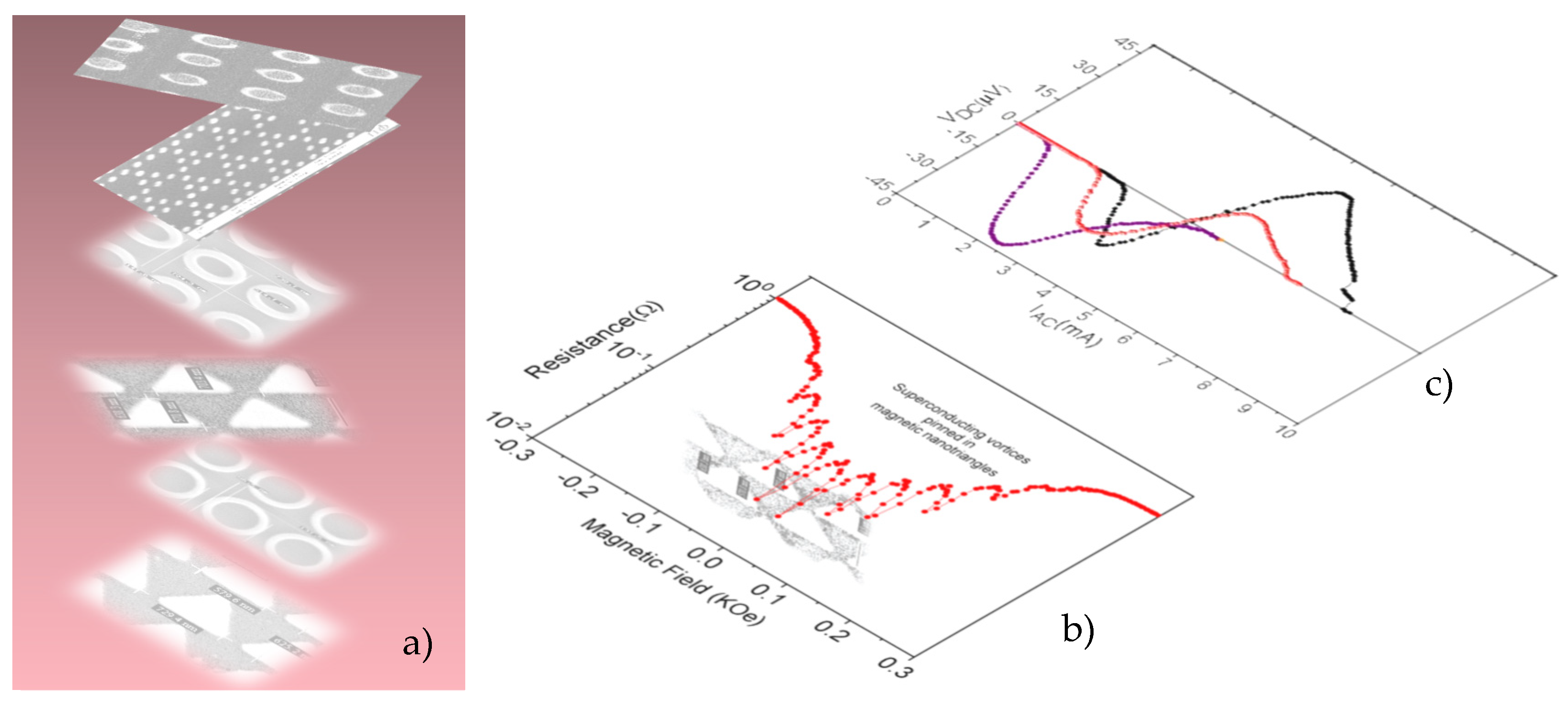
Figure 1.
Magnetic pinning center designs (a), magnetoresistance measurements (b), and ratchet effects (c) of superconducting vortices from magnetic nanostructures with different shapes in hybrid Nb/Ni superconductor/magnetic devices, from [37,38,39,40,42,43,44] Reprinted/adapted with permission from Ref. [38] © 2011 American Physical Society. Such hybrid devices represent a clear example of how superconducting and magnetic properties can be properly combined and tailored at relevant interacting length scales to achieve controllable effects, which can tune the electronic response of these devices through the superconducting–magnetic interaction at the nanoscale.

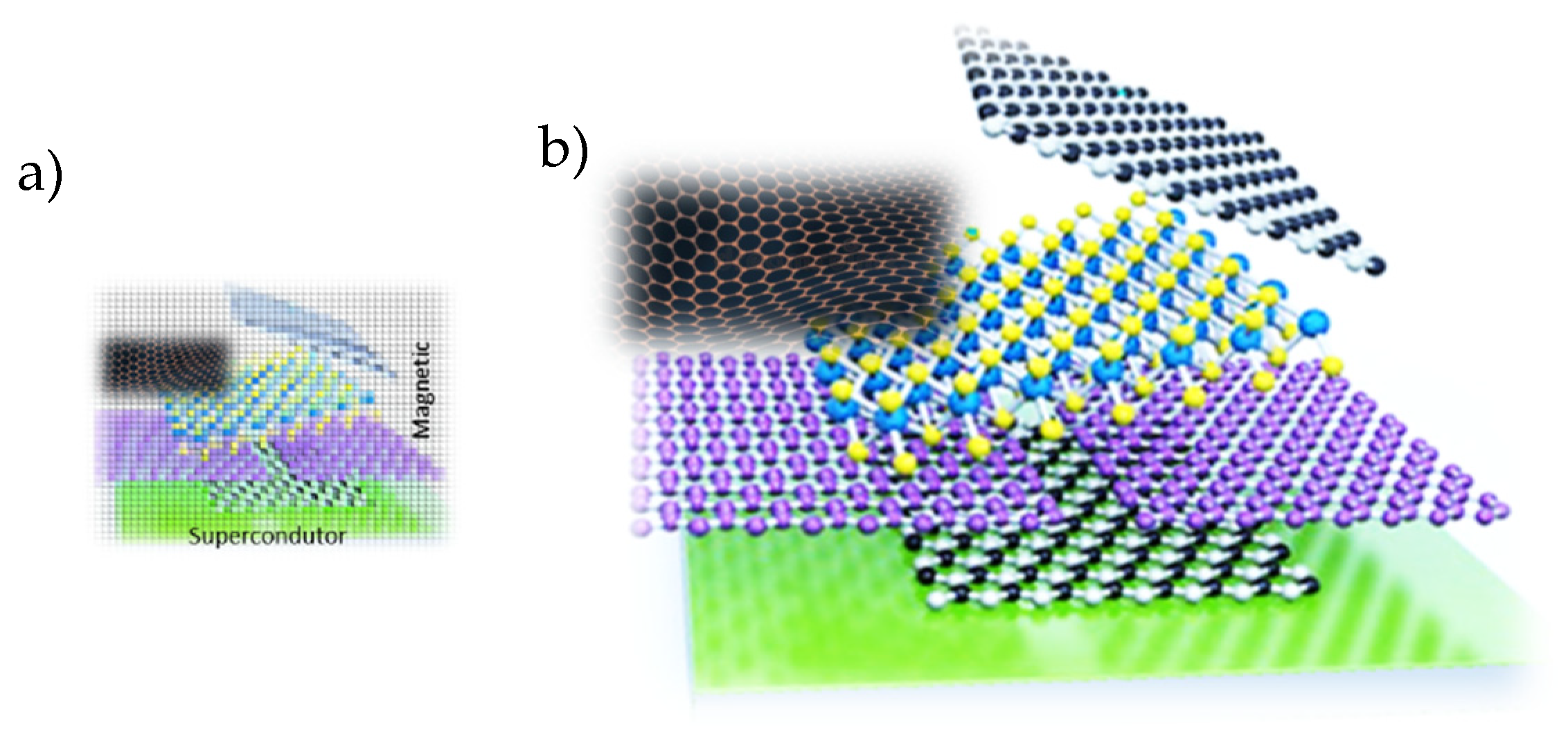
Figure 2.
Heterostructures composed of two-dimensional layers by stacking different materials with controlled rotation angles and interfaces, similar to a bitmap of multi properties obtained at will (a), to fabricate hybrid devices (b) with localized tunable magnetic and superconducting properties.
Figure 2.
Heterostructures composed of two-dimensional layers by stacking different materials with controlled rotation angles and interfaces, similar to a bitmap of multi properties obtained at will (a), to fabricate hybrid devices (b) with localized tunable magnetic and superconducting properties.

Publisher’s Note: MDPI stays neutral with regard to jurisdictional claims in published maps and institutional affiliations. |
© 2022 by the author. Licensee MDPI, Basel, Switzerland. This article is an open access article distributed under the terms and conditions of the Creative Commons Attribution (CC BY) license (https://creativecommons.org/licenses/by/4.0/).
Share and Cite
MDPI and ACS Style
Perez de Lara, D. Hybrid Superconducting/Magnetic Multifunctional Devices in Two-Dimensional Systems. Physchem 2022, 2, 347-356. https://doi.org/10.3390/physchem2040025
AMA Style
Perez de Lara D. Hybrid Superconducting/Magnetic Multifunctional Devices in Two-Dimensional Systems. Physchem. 2022; 2(4):347-356. https://doi.org/10.3390/physchem2040025
Chicago/Turabian StylePerez de Lara, David. 2022. "Hybrid Superconducting/Magnetic Multifunctional Devices in Two-Dimensional Systems" Physchem 2, no. 4: 347-356. https://doi.org/10.3390/physchem2040025