Review

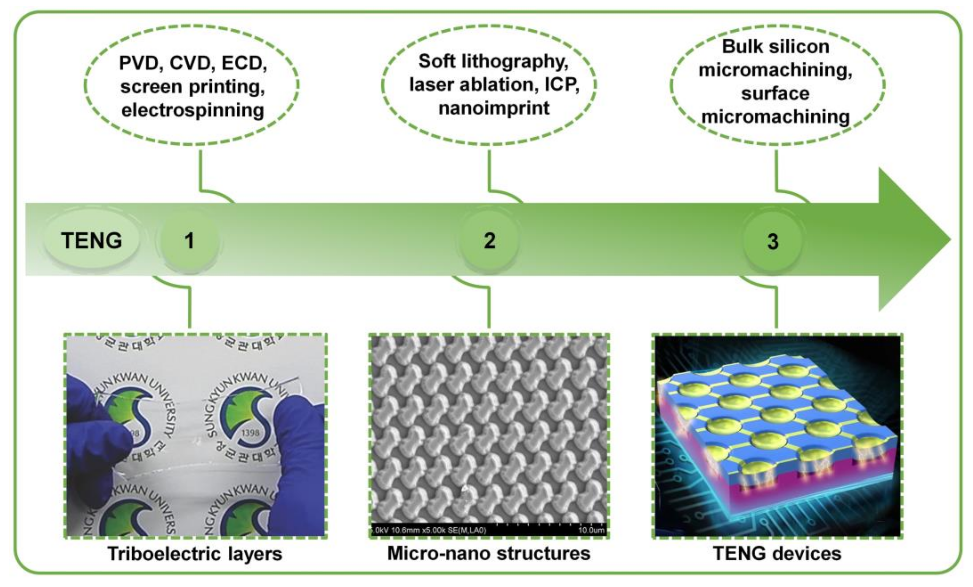
Overview of Advanced Micro-Nano Manufacturing Technologies for Triboelectric Nanogenerators

1
CAS Center for Excellence in Nanoscience, Beijing Key Laboratory of Micro-Nano Energy and Sensor, Beijing Institute of Nanoenergy and Nanosystems, Chinese Academy of Sciences, Beijing 101400, China
2
Center on Nanoenergy Research, School of Physical Science and Technology, Guangxi University, Nanning 530004, China
3
School of Nanoscience and Technology, University of Chinese Academy of Sciences, Beijing 100049, China
*
Author to whom correspondence should be addressed.
These authors contributed equally to this work.
Nanoenergy Adv. 2022, 2(4), 316-343; https://doi.org/10.3390/nanoenergyadv2040017
Submission received: 13 October 2022 / Revised: 11 November 2022 / Accepted: 21 November 2022 / Published: 25 November 2022

Abstract

:
In the era of the Internet of Things, various electronics play an important role in information interaction, in which the power supply is an urgent problem to be solved. Triboelectric nanogenerator (TENG) is an emerging mechanical energy harvesting technology that can serve as a power source for electronics, which is developing towards high performance, miniaturization and integration. Herein, the advanced micro-nano manufacturing technologies are systematically reviewed for TENGs. First, film preparation such as physical vapor deposition, chemical vapor deposition, electrochemical deposition, electrospinning and screen printing for triboelectric layers are introduced and discussed. Then, surface processing, such as soft lithography, laser ablation, inductively coupled plasma and nanoimprint for micro-nano structures on the surface of triboelectric layers are also introduced and discussed. In addition, micro-electromechanical system fabrication for TENG devices such as acoustic and vibration sensors, is introduced, and their current challenges are analyzed. Finally, the challenges of the advanced micro-nano manufacturing technologies for the TENGs are systematically summarized, and further development is prospected.

1. Introduction

With the development of the Internet of Things (IoT), electronics are connected to the IoT in increasing numbers. It is estimated that at least 30 billion objects will be linked to IoT by 2025 [1]. Generally, storage devices such as capacitors and batteries are the most common methods of driving electronics [2]. Although the advancement of microelectronic technology promotes the continuous development of electronics in the direction of miniaturization, intelligence and low energy consumption, for trillions of batteries with a limited lifetime and widespread distribution, monitoring, replacing and recycling batteries would be a vast or even impossible task [3]. A large amount of clean energy in the natural environment can be harvested to power these electronics. Among them, mechanical energy is the most widely distributed form in the environment, which is hardly affected by weather conditions and the working environment [4]. Hence, harvesting mechanical energy from the ambient environment to drive electronics is undoubtedly a feasible solution to the power supply problem. As an emerging mechanical energy harvesting technology, triboelectric nanogenerator (TENG) based on contact electrification and electrostatic induction was first proposed by Wang’s group [5], which can convert diverse forms of mechanical energy into electrical energy [6,7,8,9,10]. TENG has attracted extensive attention because of its advantages such as low cost, extensive material selection, flexible structures, light weight, and high efficiency at low operating frequencies [11,12]. Currently, various TENG structures are designed to harvest different forms of mechanical energy to provide in-situ power for many distributed electronics connected to the IoT. Wang et al. [13] proposed a flexible seaweed-like TENG to harvest wave energy and provide in-situ power for marine distributed sensors. Fu et al. [14] designed an autonomous wireless anemometer for simultaneously harvesting wind energy and wind speed sensing, which is based on a planetary rolling TENG providing in-situ power. Xu et al. [15] reported an autonomous rainfall monitoring and wireless transmission system driven by a raindrop TENG array. Nevertheless, the output performance, miniaturization and integration of TENGs limit their further development and application in microelectronics.
In the preparation of triboelectric layers, spin coating is a common method. Many materials could be spin-coated to prepare triboelectric layers, such as graphene [16], polydimethylsiloxane (PDMS) [17], polyvinylidene difluoride/polymethyl methacrylate (PVDF/PMMA) [18] and polyvinyl alcohol/lithium chloride (PVA/LiCl) [19]. However, it is difficult or even impossible to precisely control the triboelectric layers with a thickness of nanometers by the spin coating method. It is difficult to prepare the triboelectric layers by this method for some materials with excellent properties. Advanced micro-nano manufacturing technologies including chemical vapor deposition (CVD), electrochemical deposition (ECD) and physical vapor deposition (PVD), can solve the above problems to prepare high-performance triboelectric layers. Moreover, advanced micro-nano manufacturing technologies such as soft lithography, laser ablation, inductively coupled plasma (ICP) and nanoimprint can be used to fabricate micro-nano structures on the surface of the triboelectric layers. It is encouraging that advanced micro-nano manufacturing technologies can precisely control the size and thickness of TENGs, especially MEMS fabrication technology, which greatly facilitates the development and application of TENGs in microelectronics.
This review focuses on the advanced micro-nano manufacturing technologies for TENGs, as illustrated in Figure 1. In terms of advanced micro-nano manufacturing technologies, the film preparation for triboelectric layers is reviewed and discussed in Section 2. Subsequently, the surface processing for micro-nano structures on the surface of triboelectric layers is introduced and discussed in Section 3. Furthermore, the progress, issues and challenges of micro-electromechanical system (MEMS) fabrication for TENG devices (MEMS-TENGs) are introduced, analyzed and discussed in Section 4. Finally, the challenges of the advanced micro-nano manufacturing technologies for TENGs are summarized, and its potential opportunities are prospected.

2. Film Preparation for Triboelectric Layers

Various thin-film fabrication technologies have been successively used to prepare triboelectric layers. In this section, the preparation of triboelectric layers by PVD, CVD, ECD, electrospinning and screen printing is introduced and discussed.

2.1. Physical Vapor Deposition

PVD is a deposition process in which molecules or atoms are transferred to the substrate surface in the form of vapor through a low-pressure gaseous vacuum or plasma environment for condensation [23]. PVD includes techniques such as electron-beam deposition, ion plating evaporation, sputtering and vacuum thermal deposition, which can realize the thickness of the deposited layer from nanometer to millimeter. To efficiently harvest acoustic energy, the thickness of the triboelectric layer and TENG should be controlled. As shown in Figure 2a, Fan et al. [24] fabricated a paper-based TENG with a thickness of less than 125 µm using PVD deposition of Cu with a thickness of 100 nm and polytetrafluoroethylene (PTFE, 25 µm thick) as a triboelectric pair for acoustic energy harvesting. However, such a single-layer TENG may limit its application due to low output current [25]. Figure 2b exhibits a multi-layered stacked TENG (3D-TENG) based on Al and PTFE as a triboelectric pair, in which Al was deposited on both sides of flat acrylic by PVD [25]. The outputs of all TENGs can be synchronized through 3D-TENG, so that the open-circuit voltage (VOC), short-circuit current (ISC) and peak power density is 303 V, 1.14 mA and 104.6 W/m2, respectively.
Metals can be deposited not only on flat substrates but also on different shaped and patterned substrates. As illustrated in Figure 2c, Su et al. [26] deposited Cu as positive triboelectric layers on both sides of a wavy-shaped Kapton by electron beam deposition, which formed an impact-TENG with two PTFE films for harvesting water wave energy. Lee et al. [27] developed a fully packaged, ultrathin and no-spacer hemispheres-array structured TENG (H-TENG) by depositing Cu on the hemispherical PDMS array film with the function of springs to keep the upper and lower materials separated, which acts as an active self-powered sensor array for mapping the pressure distribution generated through the foot (Figure 2d). This deposition method can directly obtain the triboelectric layer with micro-nano structures without affecting the elasticity of the substrate. Metals can be deposited by PVD on flexible and non-flexible substrates with different surface structures, which makes PVD more compatible with the structural design of MEMS-TENGs.
In addition to the preparation of metal triboelectric layers, other materials have also been reported [28,29,30]. Zhang et al. [28] successfully prepared amorphous carbon (a-C) and graphene sheet embedded carbon (GSEC) thin films with 100 nm thickness on p-type silicon wafer by PVD in a plasma system. By comparing the electrical output performance and maximum instantaneous energy conversion of GSEC-based TENG and a-C-based TENG, it was found that the former was better than the latter. The cause of the high output performance of the GSEC-based TENG was believed to be the channel and edge effects of graphene sheets [28]. As illustrated in Figure 2e, Parajuli et al. [29] vacuum deposited a C60 thin film about 200 nm thick, on PET/ITO substrate by PVD technology and explored the electrical output performance of triboelectric pairs composed of the C60 film and different materials. It was determined that C60 ranked between Kapton and polyvinyl chloride (PVC) in the triboelectric series. Moreover, a novel liquid-solid TENG based on PVD fluorination modification of microarc oxidation (MAO) coating surface was constructed and designed for in-situ self-powered cathodic protection and wave energy harvesting [30]. The triboelectric layer was prepared by MAO treatment on an Al substrate followed by the deposition of 1H,1H,2H,2H-perfluorooctyltriethoxysilane using simple PVD. Although there is a wide range of materials for TENG, up to now, there have been relatively few materials for the preparation of triboelectric layers by PVD, which may be caused by poor compatibility between polymer materials with excellent triboelectric properties and PVD.

2.2. Chemical Vapor Deposition

CVD in the broadest sense refers to forming a solid film on a substrate through the chemical reaction of vapor-phase precursors [31]. A characteristic of CVD technology is its outstanding throwing power to produce a coating of low porosity and uniform thickness even on complex shaped substrates, while another important feature is the ability to locally or selectively deposit on patterned substrates [32]. Furthermore, materials with a wide range of physical, chemical and tribological properties can be grown under varying experimental conditions [32]. The above-mentioned advantages of CVD are very beneficial for the manufacturing of high-performance TENGs. Moreover, gaseous, liquid and solid raw materials can be used to prepare triboelectric layers by CVD.
A flexible, transparent and wearable TENG was constructed based on the graphene prepared by low-pressure CVD [33]. As shown in Figure 3a, large-area graphene was grown on Cu foil using a mixed gas of CH4 and H2 and successfully transferred graphene onto an EVA/PET thin film without etching the Cu foil, which is attributed to the roll-to-roll process and penetration of hot water between the graphene and native oxide layer on copper foil. Compared with other methods that require the etching of Cu to transfer the graphene, Cu can be reused in this process [20,34]. As illustrated in Figure 3b, Khan et al. [35] used a mixture of ethanol and acetonitrile as a precursor solution to prepare carbon nanotubes on a silicon wafer by a floating catalyst CVD method and then peeled off the PDMS cured on the carbon nanotubes to transfer the carbon nanotubes and designed an arc-shaped TENG for self-powered weighting using the carbon nanotubes as a negative triboelectric layer. In addition, using MoO3 and S powder as initial raw materials, the growth of a large-sized monolayer MoS2 on SiO2/Si substrate by CVD was reported by Kim et al. [36]. MoS2-based TENGs with three contacts (Schottky contact, ohmic contact and p-n junction) were utilized to explore the influence of the depletion layer on the output performance, as depicted in Figure 3c.
At present, CVD has been reported to prepare triboelectric polymer layers. An ultra-flexible contact-separation mode TENG (CS-TENG) with a transmittance of 80% and a total thickness of 5.5 μm was fabricated by CVD technology [37]. The TENG was fabricated by stacking two graphene-covered 2 μm parylene thin films layer by layer, and the serpentine structure was introduced as the spacer in one parylene thin film. The TENG shows excellent mechanical properties when triggered under different frequencies of impacts, and the response and recovery times are 20 and 50 ms, respectively. This fabrication method provides a reference for the miniaturized, integrated and standardized manufacturing of the TENGs. It is worth noting that parylene is a polymer material commonly used in the fabrication process of MEMS devices [38,39,40,41,42,43]. The thickness of the triboelectric layer is an important factor affecting the output performance of the TENG. Mariello et al. [44] prepared a parylene C film by CVD and investigated the influence of the thickness of the parylene C film on the output performance of a single-electrode mode TENG (S-TENG). As the thickness of the parylene C film increases from 1 to 6 μm, the VOC of the S-TENG decreases. Mariello et al. [44] believe that the main reason was the decrease in the capacity of the S-TENG and the increase in rigidity of the layered structure. The ability of CVD to effectively control the thickness of polymer films is of great significance for the fabrication of ultra-thin TENGs and MEMS-TENGs.

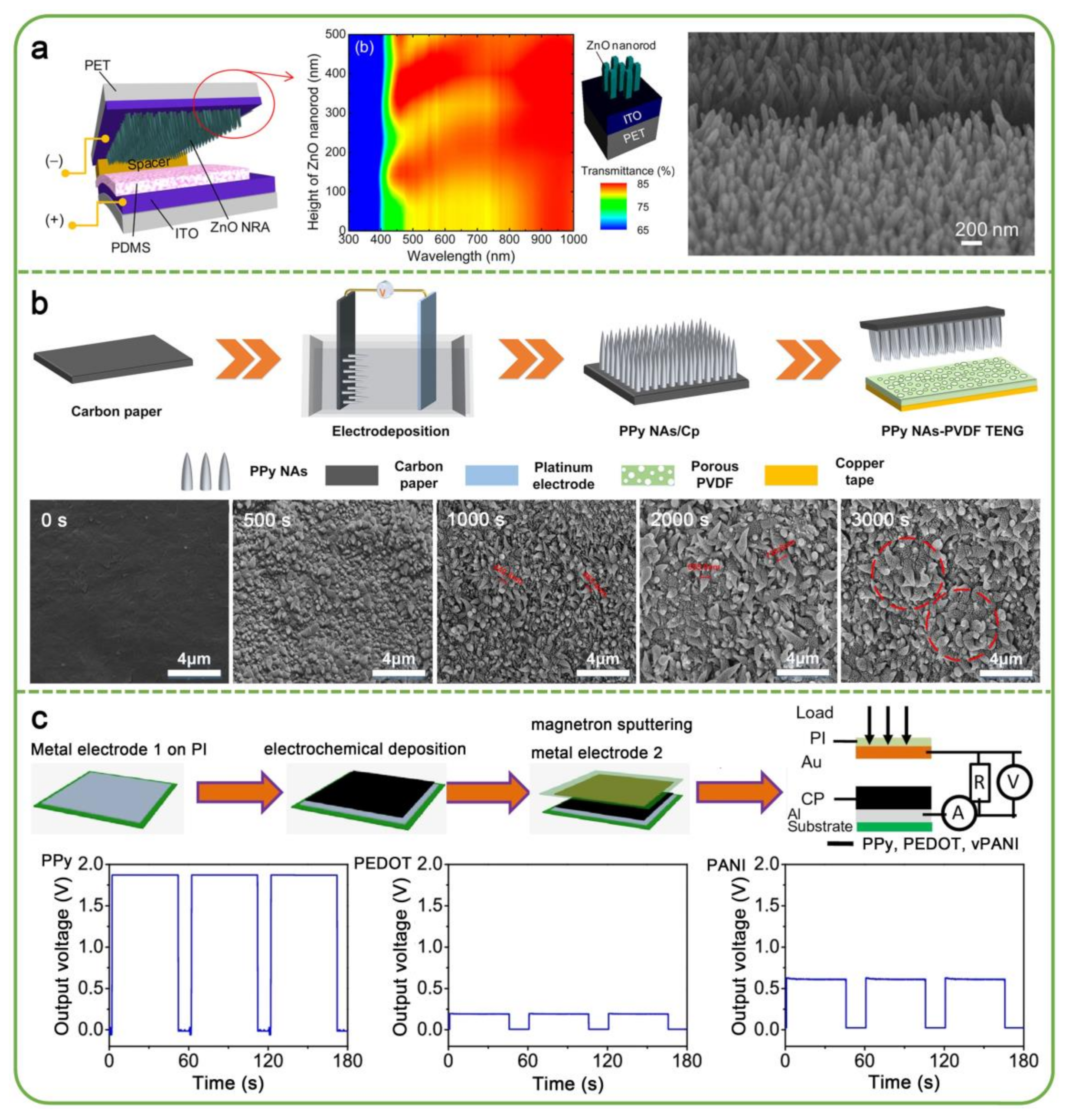
2.3. Electrochemical Deposition

ECD is a technology in which positive and negative ions migrate in an electrolyte solution under the action of an applied electric field, and then a redox reaction occurs on electrodes to form a coating [45]. ECD is a commonly used technology in the manufacturing of MEMS devices, which is used to prepare conductive materials, especially metal materials. Therefore, ECD requires the preparation of thin films on conductive substrates, and pre-deposition of a metal seed layer is usually required for insulating substrates to prepare triboelectric layers.
Triboelectric layers with micro-nano array structures can be directly prepared on a flat substrate by ECD without further processing. As shown in Figure 4a, the vertical growth of ZnO nanorod arrays (NRAs) on ITO/PET flexible substrate by ECD was reported by Ko et al. [46], which formed a transparent TENG with PDMS. Compared with conventional ITO/PET, ZnO NRAs significantly reduced the reflectance from 20% to 9.7% at a wavelength range of 300–1100 nm. In addition, 3D polypyrrole nanoarrays (PPy NAs) prepared by ECD were also used as a triboelectric layer combined with porous PVDF to fabricate a wearable TENG [47]. Figure 4b demonstrates the effect of different deposition times on the morphology of 3D PPy NAs. With the increase in deposition time, the obtained PPy NAs appeared to coarsen and gradually grew into a 3D conical microstructure, then the diameter size further increased, and finally, agglomeration occurred. When the deposition time was 1000 s, the effective contact area between PPy NAs and porous PVDF is the largest; thereby the output performance of the wearable TENG was the best.
Conductive polymers can be used not only as triboelectric layers of alternating current TENGs (AC-TENGs), but also for direct current TENGs (DC-TENGs). Meng et al. [48] employed ECD to deposit PPy, polyethoxythiophene (PEDOT) and polyaniline (PANI) on metal electrodes, and explored the output performance of the DC-TENGs with each of them as the triboelectric layer, respectively. As depicted in Figure 4c, the output voltages of the DC-TENG based on Au/PPy/Al (left), Au/PEDOT/Al (middle) and Cu/PANI/Al (right) are 1.85, 0.2 and 0.6 V, respectively.
Similar to PVD and CVD, ECD can also deposit a triboelectric layer on micro-nano structured substrates. Mariappan et al. [49] deposited antimonene on 3D nickel foam as a triboelectric layer by ECD, and Raman mapping and X-ray photoelectron spectroscopy (XPS) confirmed that the thickness of the antimonene nanostructure is less than 20 nm. It was used in a TENG with Kapton as the negative triboelectric layer, and the VOC, ISC and peak power are 54 V, 0.87 μA and 15 μW, respectively. Although ECD is limited in the choice of substrates and triboelectric materials, it has shown great application prospects in the manufacturing of DC-TENGs.

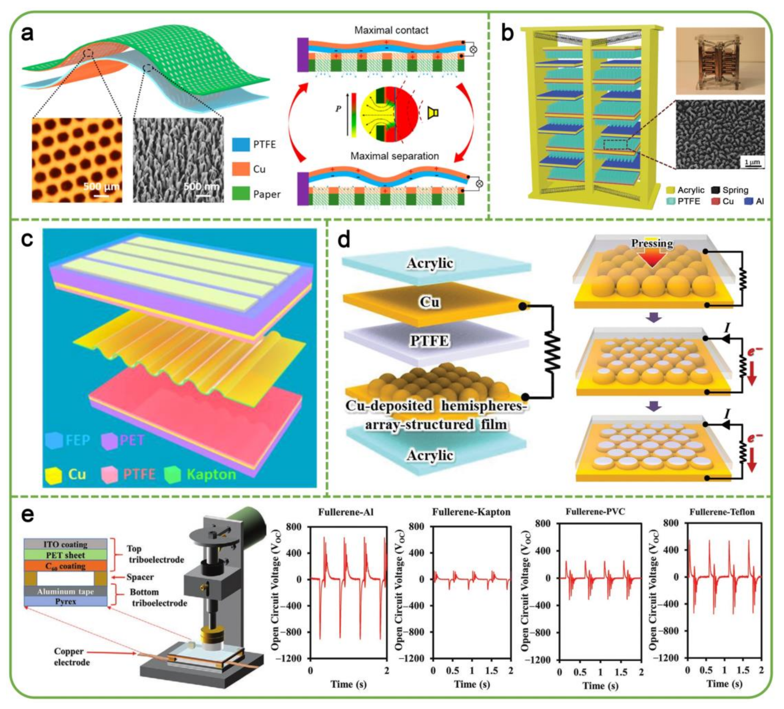
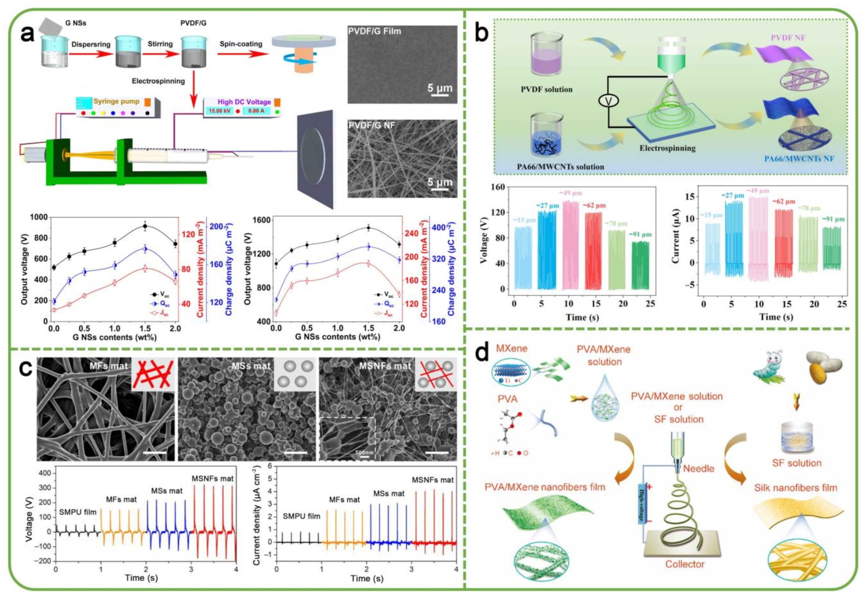
2.4. Electrospinning

Electrospinning is a fiber fabrication process in which a polymer solution or melt is jet-spun in a strong electric field [50]. The main components of electrospinning include a high-voltage power supply (direct current or alternating current), a syringe pump, a spinneret and a conductive collector [51]. When energized, electrostatic repulsion between surface charges with the same sign transforms the droplet into a Taylor cone, and then a charged jet is ejected from the cone, and when the jet is stretched to a finer diameter, it solidifies rapidly, resulting in solid fibers deposited in a grounded collector [52].
Electrospinning can directly prepare the triboelectric layers with surface micro-nano structures without additional processing, which makes it popular in TENG manufacturing [53,54,55,56]. Figure 5a shows the preparation process of PVDF/Graphene nanosheet (G NS) hybrid films through spin coating and electrospinning technology [57]. PVDF/G NF obtained by electrospinning has an obvious fibrous structure, while the surface of the other film is relatively flat. Compared with a PVDF/G film, the TENG composed of PVDF/G NF and polyamide-6 (PA6) film has higher output performance, with an output voltage of 1511 V, a short-circuit current density (JSC) of 189 mA/m2, and a peak power density of 130.2 W/m2. The thickness of the triboelectric layer can be effectively controlled by setting the spinning time, which is conducive to further improving the output performance of the TENG. As depicted in Figure 5b, Sun et al. [58] prepared PA66/multi-walled carbon nanotubes (MWCNTs) and PVDF nanofiber membranes by electrospinning technology, which acts as positive and negative triboelectric layers of nanofiber-based TENG (NF-TENG), respectively. To improve the output performance of the NF-TENG, the thickness of PA66/MWCNTs nanofiber membrane was optimized in the range of 15 to 90 µm. When the thickness of PA66/MWCNTs nanofiber film is 49 µm, the VOC and ISC of NF-TENG reach their maximum. Furthermore, the spinning time will affect the light transmittance of the triboelectric layer [59]. Therefore, the spinning time is a noteworthy factor when fabricating a transparent TENG.
The micro-nano structures of the surface of the triboelectric layers can also be adjusted by controlling the viscosity or concentration of the electrospinning solutions while preparing the triboelectric layers. As shown in Figure 5c, Xiong et al. [60] successfully prepared microfibers (MFs), microspheres (MSs) and microsphere-nanofibers (MSNFs) by adjusting the viscosity of the ether-based thermoplastic Tg-type shape memory polyurethane (SMPU) with dimethylformamide solvent. MF mats can be produced by electrospinning in SMPU solutions with a viscosity greater than or equal to 1973 cP, MS mats can be prepared in polymer solutions with a viscosity that does not exceed 41.6 cP, and MSNF mats can be obtained from polymer solutions with a viscosity of 41.6–1973 cP. The output performances of different TENGs based on SMPU and Al were in the order of SMPU film-TENG < MFs mat-TENG < MSs mat-TENG < MSNFs mat-TENG. Moreover, the triboelectric layers with different surface micro-nano structures can be prepared by electrospinning with different P(VDF-TrFE) concentrations [61]. As the concentration increased from 4 to 10 wt%, a large number of small particles appeared in electrospinning P(VDF-TrFE) accompanied by the formation and disappearance of the honeycomb structure, which is considered to be caused by the weakening of the effect of surface tension. However, when the concentration increased to 15 wt%, the typical nanofiber structure appeared, which is due to the high viscosity of the solution and the easy evaporation of the solvent.
Both positive and negative triboelectric layers can be prepared by electrospinning during TENG fabrication [62]. An all-electrospun flexible TENG (PE-TENG) with a multilayered nanofiber structure for enhanced output performance was reported [63]. Among them, PVDF, PVA, carbon black-doped polystyrene nanoparticles (PSC) and polystyrene (PS) were all fabricated by electrospinning, which was used as a negative triboelectric layer, a positive triboelectric material, a conductive interface layer and an electron barrier layer, respectively. The PSC accelerates the charge transfer rate, and the PS provides high electron trapping holes, further increasing the charge density, thereby enhancing the output of the PE-TENG. In addition, a variety of materials can be mixed in the electrospinning solution to improve the properties of the triboelectric layer prepared by electrospinning [64,65,66]. Jiang et al. [67] reported an all-electrospun flexible TENG in which polyvinyl alcohol (PVA) was mixed with an MXene nanosheet material with high electronegativity and conductivity by electrospinning to prepare the nanofiber film as a negative triboelectric layer and silk fibroin (SF) as a positive triboelectric layer. The instantaneous peak power density of the fabricated TENG reached 1087.6 mW/m2. Therefore, electrospinning is a very competitive technology in the preparation of high-performance triboelectric layers.

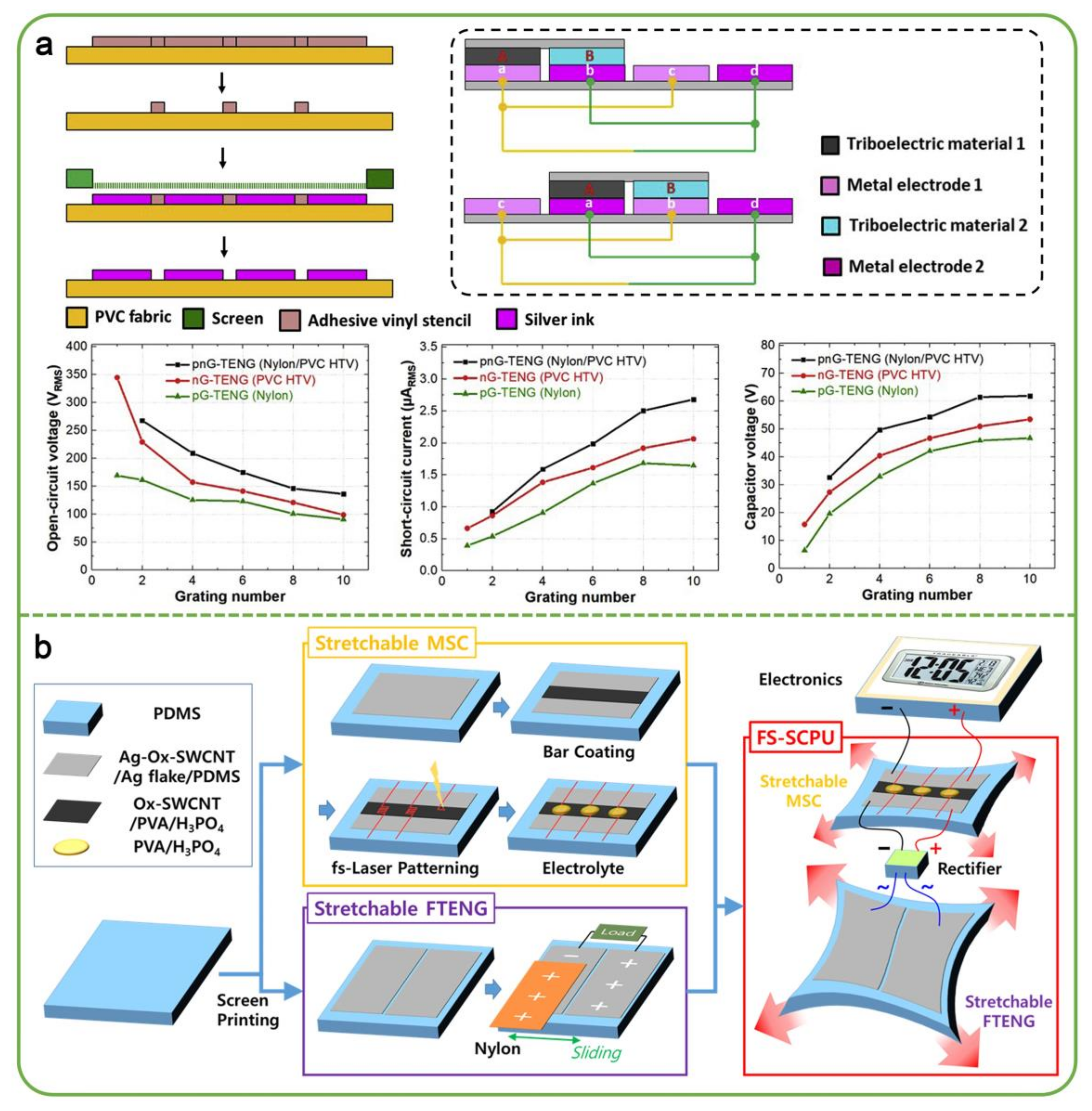
2.5. Screen Printing

Screen printing is a printing technology that transfers ink onto a rigid or flexible substrate to obtain a specific pattern through a printing process. It has the advantages of easy operation, low cost, simple fabrication process and large-scale production [68,69]. It is considered a highly competitive fabrication technology for the rapid and scalable fabrication of printed microelectronics [70]. Currently, materials such as Ag, ZnO, La2O3 and carbon nanotubes have been used to fabricate triboelectric layers by screen printing [71,72,73]. The desired patterned triboelectric layer can be obtained by designing the mask. To improve the breathability of a wearable TENG, electrospinning and screen-printing, batch-scale fabrication technologies were used to fabricate a self-powered nanofiber-based triboelectric sensor (SNTS) for health monitoring [71]. The stacking of electrospun PVDF nanofibers and the screen-printed silver nanoparticles ensure the gas channel throughout the device, and the air permeability of SNTS is up to 6.16 mm/s. As depicted in Figure 6a, Paosangthong et al. [74] reported a free-standing mode TENG (pnG-TENG) with alternating positive and negative grating structures, which consists of a triboelectric layer prepared by screen printing with an Ag ink, a positive triboelectric layer (nylon fabric) and a negative triboelectric layer (polyvinyl chloride heat transfer vinyl, PVC HTV) alternately. Compared with single nylon (pG-TENGs), single PVC HTV (nG-TENGs) and grating-free TENG, the performance of pnG-TENG is significantly improved. The ISC and capacitor charging voltage of the pnG-TENG increased with the number of gratings, while the VOC decreased with the increase in the capacitance of the electrodes. Furthermore, the VOC and ISC of the pnG-TENG are theoretically equal to the sum of the VOC and ISC of the pG-TENG and nG-TENG. The VOC, ISC and maximum power of the pnG-TENG are 136 V, 2.68 μA, and 125 μW, respectively. The maximum power density of the pnG-TENG reached 38.8 mW/m2, which is 6.43 and 1.94 times higher than that of the grating-free TENG and nG-TENG, respectively. During the preparation of the triboelectric layer, the Ag layer obtained after screen printing can be heated to get a uniformly wrinkled surface, which effectively improves the contact area [75]. Prutvi et al. [76] reported a self-powered vibration sensor based on an S-TENG, in which a ZnO film is prepared by screen printing as a positive triboelectric layer and an FEP film as a negative triboelectric layer. At resonance, the peak-to-peak voltage, ISC and power density generated by the S-TENG are 25 V, 10 μA and 1.38 W/m2. The vibration sensor has an accuracy of >99% in the wide frequency range of 0–400 Hz, and the maximum sensitivity was 14 V/g. In addition, a La2O3 nanocrystal with a large surface area was used to fabricate a triboelectric layer through a screen-printing process [73]. The VOC and ISC of the TENG composed of La2O3 and PTFE are 120 V and 23.7 µA, respectively. With an external load resistance of 30 MΩ, the maximum power density was up to 7.125 W/m2. To develop a stretchable self-charging power unit for harvesting and storing energy, Yang et al. [77] fabricated a micro-supercapacitor (MSC) and a stretchable TENG on PDMS substrates using screen printing technology; it is displayed in Figure 6b. The maximum instantaneous power density of the TENG is 84.4 mW/m2, and the performance did not decrease significantly when stretched up to 40%. Integrating TENG and MSC can serve as a fully stretchable self-charging power unit (FS-SCPU) for wearable electronics. Screen printing is an effective way for the large-scale preparation of triboelectric layers, but the thickness of the triboelectric layers is difficult to precisely control, which, to some extent, affects its application in specific TENG structures.

3. Surface Processing for Micro-Nano Structures

Increasing the effective contact area of the contact electrification process by fabricating surface micro-nano structures of the triboelectric layers is a way to enhance the output performance of TENGs. Soft lithography, laser ablation, ICP and nanoimprinting are commonly used technologies for fabricating surface micro-nano structures. In this section, their applications in the TENGs manufacturing process are introduced and discussed.

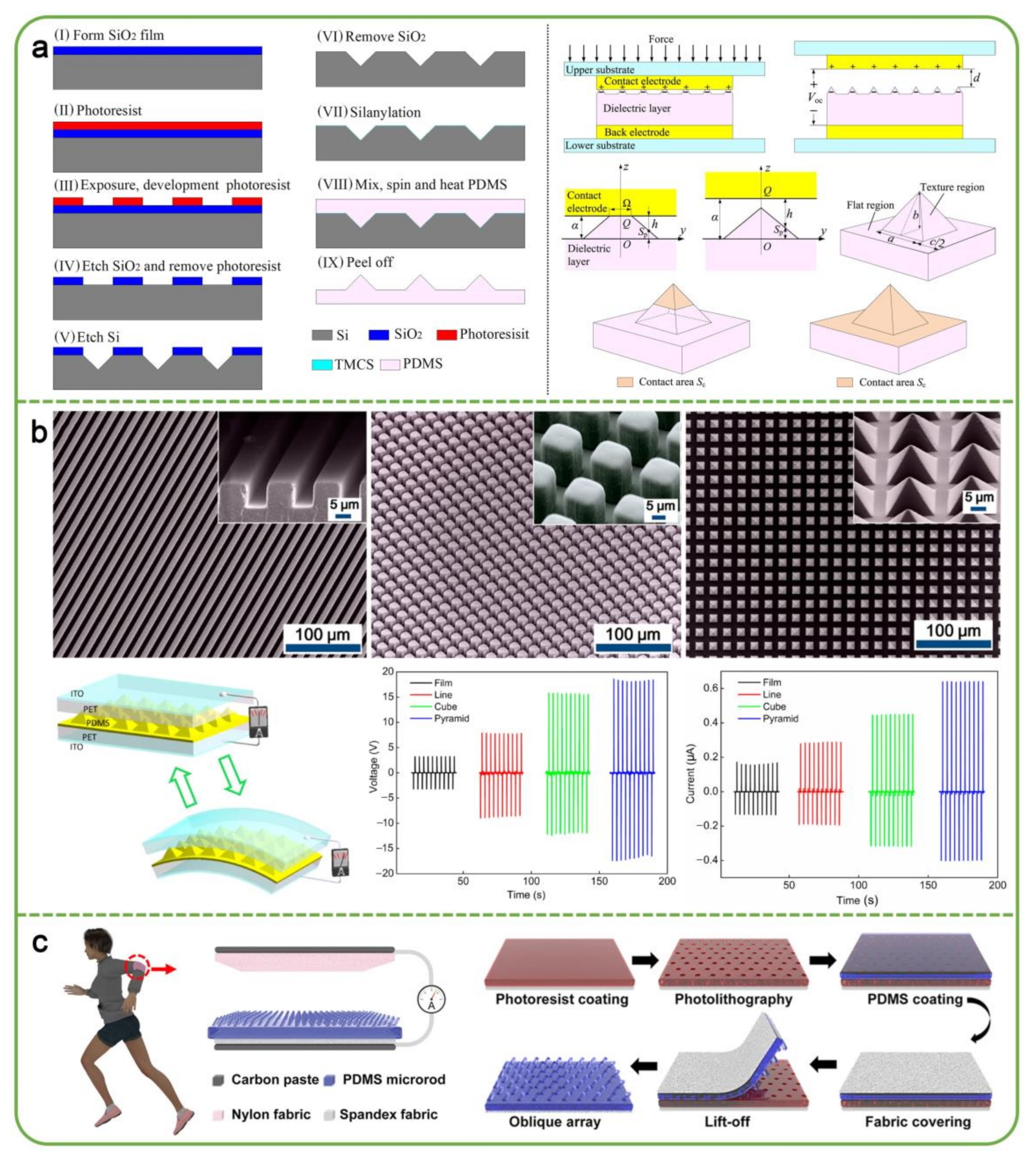
3.1. Soft Lithography
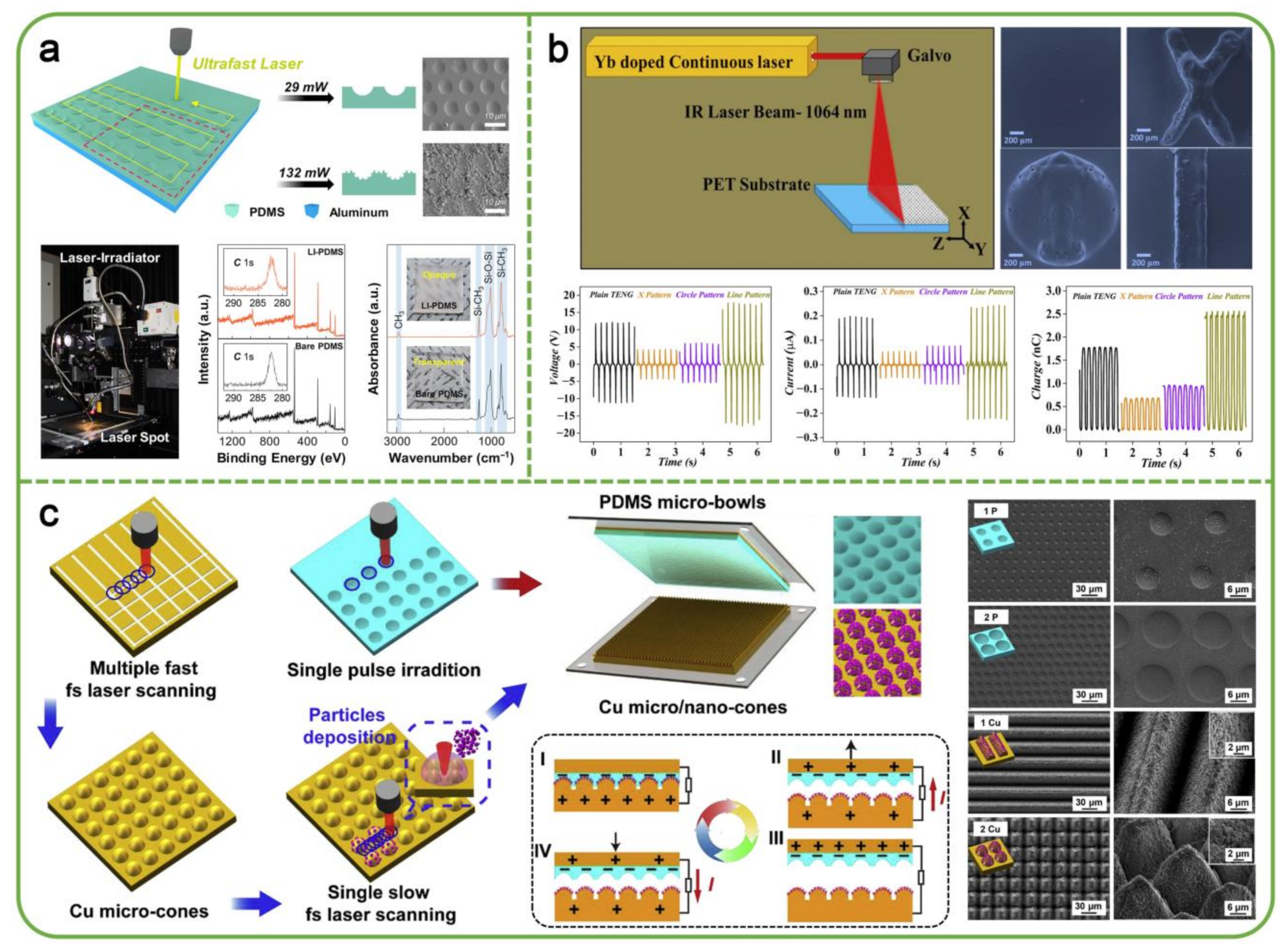
Soft lithography is a micro-pattern replication technology; it includes micromolding in capillaries, replica molding, microcontact printing, solvent-assisted micromolding and micro-transfer molding, in which the manufacture of elastomeric stamps is an important step. PDMS, polyimide (PI) and polyurethane are common elastomeric stamps. PDMS is a commonly used triboelectric material, which can also be engraved with UV light to create patterns on its surface [78,79]. To quantitatively analyze the “effective” contact area of micro-nano structures, Yang et al. [80] fabricated the pyramid-textured surface of TENG by technologies such as photolithography, wet etching and replication, and then adopted the inexact Newton method, bi-conjugate stabilized method and fast Fourier transform (FFT) technique to quantitatively analyze the effect of texture size and applied force on the effective contact area and VOC. Figure 7a shows the fabrication process of the textured PDMS layer and a theoretical model of the contacting process. The four sides of the pyramid pattern participate in contact electrification, so the effective contact area should be the sum of the contact area of the pyramid lateral only with the texture area contact. When both the pyramid texture and the flat regions were in contact, the effective contact area was the sum of the contact area on the four sides of the pyramid and the flat contact area. The VOC of TENG with a pyramid texture increases owing to the increase in the effective contact area under smaller pressure, while under larger pressure, the VOC remains stable due to the constant contact area. In addition, the contact area and VOC of the TENG increase with the increase in texture pitch under smaller pressure and decreases with the increase in texture pitch under larger pressure.
The output performance of TENGs is different owing to the difference in the effective contact area of different-patterned triboelectric layers during contact electrification. Therefore, the output performance of TENGs can be further enhanced by optimizing the pattern of the triboelectric layer surface. Three kinds of PDMS with different surface micro-nano structures were fabricated by replication technology, and the SEM images are shown in Figure 7b [81]. The triboelectric pairs of PET and different patterned PDMS were formed, and the effect of surface micro-nano structures on the output performance of TENGs was investigated. The VOC and ISC of different TENGs are in the same order, which is flat-TENG < line-TENG < cube-TENG < pyramid-TENG. Photoresists after photolithography can also be used as a mold to prepare a triboelectric layer with surface micro-nano structures. Figure 7c demonstrates a textile-based wearable TENG (WTNG) based on an oblique PDMS microrod array [82]. The PDMS with an oblique microrod array was prepared by using a photoresist as a mold. The oblique PDMS microrods were compelled to slide and bend in one direction during the operating state, which can enhance the effective contact area of the WTNG. The VOC, JSC and maximum peak power density generated by the WTNG reached 1014.2 V, 3.24 μA/cm2 and 211.7 μW/cm2, respectively. Furthermore, photoresists with micro-nano structures can be used as a substrate to directly fabricate a patterned triboelectric layer by depositing triboelectric materials. Dhakar et al. [83] spin-coated a layer of SU-8 (negative photoresist) with a thickness of 50 µm on a silicon substrate, then used the SU-8 micropillars obtained after exposure as a substrate, and used thermal evaporation to deposit Au on the substrate to directly obtain the triboelectric layer with micropillar structures. For photolithography, various patterned triboelectric layers can be fabricated by designing masks. After exposure and development, the substrates can be processed by etching to obtain a specially patterned triboelectric layer or the desired mold for structure replication, which promotes the diversification of the surface micro-nano structures of the triboelectric layers.

3.2. Laser Ablation

Laser ablation primarily uses the photothermal effect caused by a focused laser to remotely generate a highly controllable confined temperature field at the desired location [84,85,86]. As a microfabrication technology, it has the advantages of being fast, cost-effective, scalable and environmentally-friendly, permitting in situ processing, and precise control of the surface structure of materials [87]. Surface micro-nano structures of the triboelectric layers can be changed by adjusting the laser power. Xiao et al. [88] treated PDMS surfaces with laser powers of 50, 100, 150 and 200 mW and found that the size of the hierarchical micro-nano structures decreased with the increase in laser power, resulting in a more intense thermal shock to the surface of PDMS. The contact angle of the PDMS surface prepared under 200 mW laser power is in the superhydrophobic range, which is beneficial for the construction of surface self-cleaning TENGs. Moreover, the regular surface structure was obtained by laser ablation, and the effect of laser ablation on the surface chemical composition of the triboelectric layer was investigated [89]. As shown in Figure 8a, when the laser power was 29 mW, the PDMS film surface formed a regular concave hemispherical structure, while the laser pulse over 50 mW could induce regular and deep hemispherical concave morphology and induce irregular submorphology. Under ultrafast laser irradiation, the formation of the dense electron-hole plasma destroys the chemical bonds on the surface of PDMS to create a non-thermally molten layer, and then an amorphous process is enabled to enclose the amorphous atomistic structure, which essentially dominates the PDMS surface, resulting in a rough surface with irregular submorphology at the nanoscale. XPS and Fourier-transform infrared spectroscopy (FT-IR) characterization results confirmed that the chemical composition of PDMS did not change before and after laser irradiation. In the range of 0–132 mW, the TENG achieved the maximum power output with a laser power of 29 mW.
Figure 8b exhibits the formation of different micropatterns on PET substrates using a continuous wave fiber laser with a wavelength of 1064 nm, and the effect of different surface structures on the TENG output performance was investigated [90]. Compared with the pristine and other patterned TENGs, the line-patterned TENG showed better output performance, which generated the VOC, ISC and power density of 36 V, 0.46 μA and 0.8 μW/cm2, respectively. However, the output performance of the line-patterned TENG was reported to be smaller compared to square and hexagonal patterns [91]. Cho et al. [91] directly sculpted different surface patterns (line, hexagon, and square) on PI films using a direct UV laser ablation technique that allows the accurate construction of predesigned patterns within one minute. The output performance order of the film-sponge coupled TENG based on PI and SRPA (silicone rubber and non-woven polyamide sponge) is H-sq > H-hex > H-line > L-sq > L-hex > pristine >L-line (H means a large amount, while L means a small amount). The synergistic effect in the TENG improves the output performance and exhibits good durability. In addition, Wang et al. [92] increased the surface roughness by irradiating PTFE with a femtosecond laser to improve the surface charge density and proposed a self-powered ammonia sensor based on the TENG.
The fabrication of patterns on metal surfaces by laser ablation has also been reported [93]. As illustrated in Figure 8c, a micro-nano structure-enhanced TENG was developed by Huang et al. [94], in which the laser scanning ablation technology was used to fabricate strip-like and cone-shaped micro-nano scale structures, and the micro-bowl structures with different sizes were fabricated on PDMS surfaces by single-pulse laser irradiation. The power density of the TENG with the micro-bowl structure on the PDMS surface and cone structure on the Cu surface is increased by about 21 times. Furthermore, a Q-switched pulsed laser used to etch the surface of the aluminum film can increase the VOC from 80 to 130 V and the ISC from 3.9 to 6.6 µA [95]. The spring-assisted TENG generates 66 V, 5.1 µA and 350 µW of VOC, ISC and power in the vertical vibration mode of operation at an average velocity of 10 cm/s, respectively. In addition to using laser ablation technology to directly pattern the surface of the triboelectric layers, the substrate, after laser ablation, can also be used as a mold to fabricate the surface micro-nano structures of the triboelectric layer [96,97]. Despite laser ablation having many advantages, it is limited to large-scale manufacturing.

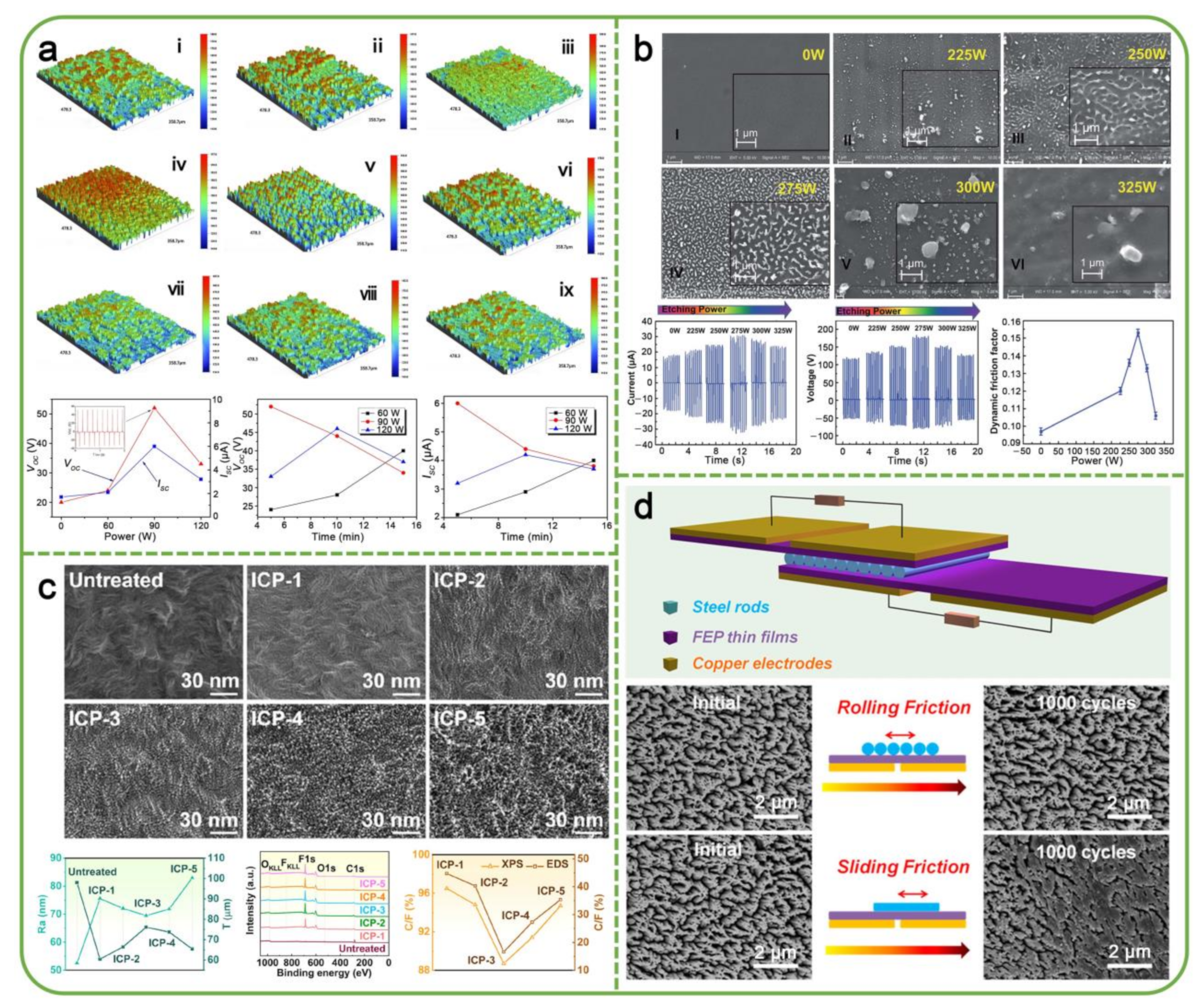
3.3. Inductively Coupled Plasma
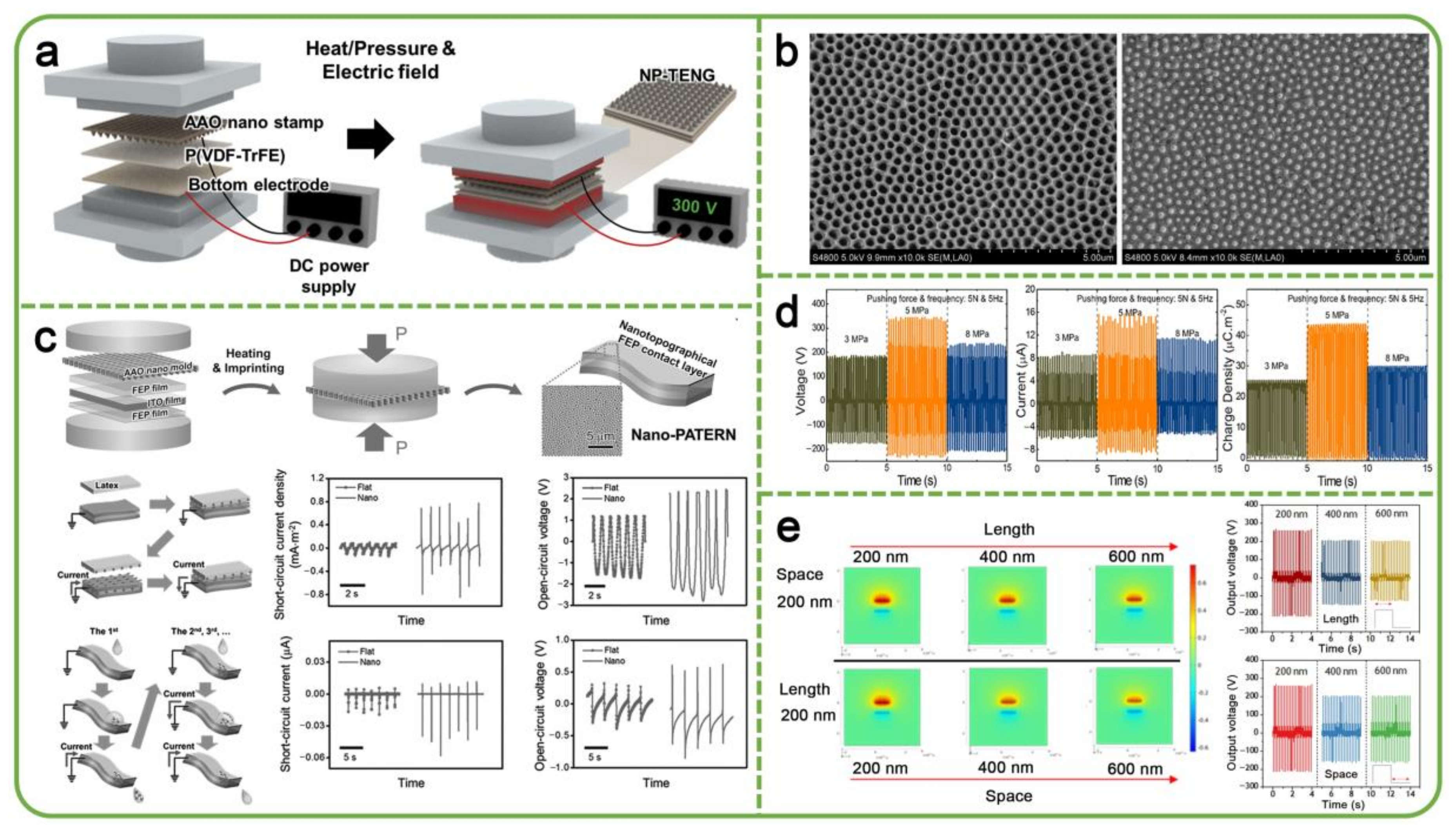
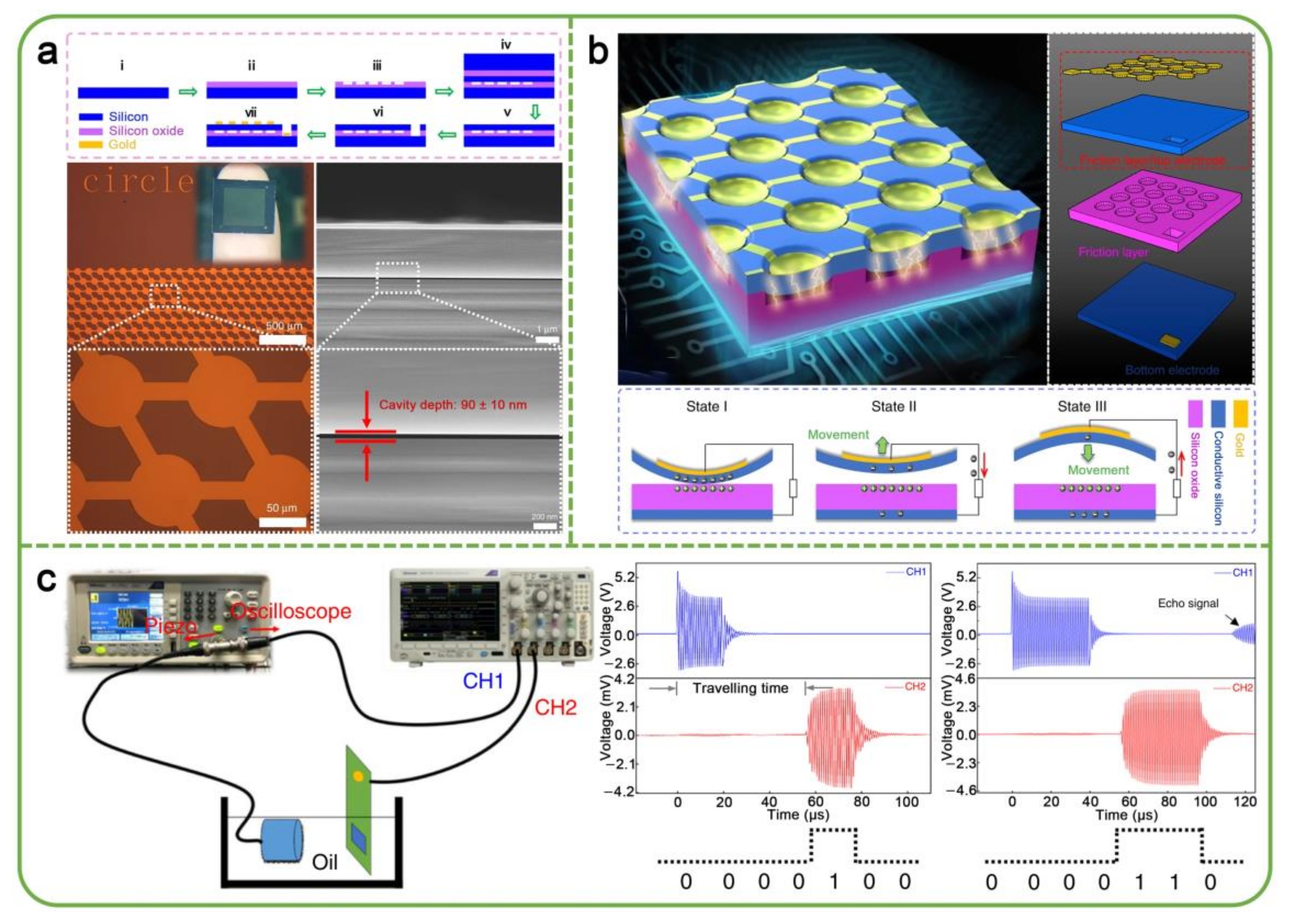
ICP means that the working gas is ionized under the excitation of an electric field and generates plasma. Since the plasma contains ions, electrons, excited atoms, molecules, free radicals, and other active particles, these active particles can react with the material to be etched. ICP is an important dry etching technology in micro-nano manufacturing, which can be etched onto the surface of thin films to form micro-nano structures. In the manufacturing process of TENGs, ICP is often used to etch the surface of the triboelectric layers to produce micro-nano structures, thus improving the output performance [98,99,100,101]. A two-step plasma etching method using O2 and Ar to increase the surface area of FTFE from 25.78 to 48.91 µm2 without CF4 gas was reported by Prada et al. [102]. After plasma treatment, the surface roughness of PTFE increases and exhibits superhydrophobic characteristics. Compared with the pristine PTFE and other plasma processes, the TENG constructed with O2/Ar treated PTFE as a triboelectric layer has better output performance. During ICP treatment, different parameters will have different effects on the surface micro-nano structures of the triboelectric layer. Cheng et al. [103] treated the PDMS surface with different ICP powers and etching times and explored the effect of different experimental conditions on the PDMS surface morphology and TENG output performance, as shown in Figure 9a. Although the surface morphologies of PDMS treated by ICP with different power are completely different, their average surface roughness has little change. Compared with the PDMS treated at 60 and 120 W, the 90-W-treated PDMS has many micropillars. The 90-W-treated PDMS (5 min) has the maximum output voltage and current. Similarly, Wang et al. [104] also utilized different ICP power to etch the surface of the triboelectric layers to optimize the output performance of the TENG. As depicted in Figure 9b, with the increase in etching power from 0 to 275 W, the surface micro-nano structure density of the ethyl cellulose (EC) films increases gradually. Whereas, as the etching power is further increased, the micro-nano structures are significantly reduced, which is due to the limitation of the thermal stability of the EC films and the high etching power to destroy the surface structure of the EC films. The EC treated with 275 W etching power as the triboelectric layer reached the maximum for VOC, ISC and dynamic friction factor. In addition, Zhang et al. [10] used O2, CHF3 (first step) and C4F8 (second step) as working gases and studied the influence of different radio frequency (RF) power on the surface micro-nano structures and chemical composition of polyethylene (PE) film under the condition of ICP power of 100 W, and proposed a TENG (RDE-TENG) for harvesting raindrop energy by using the PE film after plasma etching as a negative triboelectric layer. As depicted in Figure 9c, the average thickness (T) of the ICP-treated PE film increases first and then decreases as the RF power increases from 0 to 100 W, while the arithmetic means roughness (Ra) changes in the opposite direction. When the RF power is 50 W, the PE film (ICP-3) has a more nanotextured structure. The characterization results of XPS and energy dispersive spectrometer showed that the C/F ratio of the ICP-3 film is the lowest (the content of F is the highest), which effectively enhanced the tribo-electronegativity of the ICP-3 film and is beneficial for enhancing the output performance of RDE-TENG.
ICP can fabricate various micro-nano structures through masks, especially in the manufacturing process of MEMS devices. In the ICP etching process, metal (Al, Cu, Au, Ti, etc.) films are usually used as masks to fabricate micro-nano structures on the surface of the triboelectric layer [105,106,107,108]. Lin et al. [109] deposited a thin Au film on the FEP surface as a mask to fabricate nanowire structures by ICP etching and designed a rolling TENG using the FEP as a triboelectric layer. Figure 9d shows the structure of the rolling TENG, which consists of a set of rolled steel bars sandwiched between two FEP films. Compared to sliding friction, the surface nanowire structures of the FEP did not change significantly after 1000 cycles of rolling friction, which would prolong the service life of the TENG and ensure the output performance. Interestingly, ICP can also be used to prepare a polymer triboelectric layer while fabricating micro-nano structures [110]. As a micro-nano fabrication technology, ICP has many reports on the fabrication of micro-nano structures on the surface of the triboelectric layer, which is a promising technology for manufacturing MEMS-TENGs.

3.4. Nanoimprint

Nanoimprint technology is a replication process for micro-nano structures first proposed by Chou’s group [111], which has the advantages of high resolution, low cost and high throughput [112]. A hard mold containing nanoscale surface relief features is pressed into the polymer material and cast onto the substrate under controlled pressure and temperature, thereby creating a thickness contrast in the polymer material [113]. As illustrated in Figure 10a, Yoo et al. [114] reported a thermal nanoimprint and simultaneous electric poling approach to enhance the output performance of the TENG with a ferroelectric thermoplastic polymer and used it to harvest wind energy. Specifically, the polished aluminum substrate was immersed in 0.1 M phosphoric acids, anodized at a constant voltage of 187 V to prepare anodic aluminum oxide (AAO) nanostamps with regularly arranged nanopore arrays and used as a mold to fabricate micro-nano structures on P(VDF-TrFE) film. Figure 10b demonstrates the SEM of the porous Al2O3 as a mold and the PDMS nanopillar arrays obtained after nanoimprinting [115]. The high-resolution micro-nano structures increase the surface roughness and effective contact area of the PDMS triboelectric layer, thereby enhancing the output performance of the TENG. Moreover, Choi et al. [116] utilized AAO as a mold to fabricate micro-nano structures on a thermoplastic PET surface by thermal nanoimprint, which is displayed in Figure 10c. Compared with the TENG without micro-nano structures, the solid–solid and solid–liquid contact TENGs based on the patterned PET exhibit higher output performance.
Generally, the materials used as molds are subjected to high temperature and high pressure without changing their properties. Silicon substrates are common molds, which can obtain various patterns for nanoimprinting through photolithography. Mahmud et al. [117] successfully replicated nanopatterns of lines, pillars and hexagonal cones on PMMA and PDMS layers by thermal nanoimprinting with Si as the master stamp. The output performance of the TENG with a hexagonal cone pattern is better than other patterns, and its voltage, current density and maximum output power are 3, 6 and 22 times higher than a TENG without a pattern, respectively. The output performance of the patterned TENG can be further improved by optimizing the height, width and spacing of the patterns. The pressure applied during the nanoimprint process would affect the height of the surface pattern of the triboelectric layer [118]. Figure 10d reveals the influence of imprint pressure on the TENG output performance during the PTFE imprint process. When the pressure is 5 MPa, the VOC, ISC and charge density of TENG all reached maximum values. Kim et al. [119] utilized nanoimprinting to fabricate a defect-free and large-area nanopatterned TENG, and studied the effect of the length and space of the surface line structures of the triboelectric layer on the output performance of the TENG in detail. As illustrated in Figure 10e, when the line length and space are both 200 nm, the output voltage of the TENG reaches its maximum, which is consistent with the results of the finite element simulation. What is more, the output voltage of the TENG can be further improved by patterning the surface of another triboelectric layer. It is worth noting that nanoimprint technology can also fabricate micro-nano structures on metal surfaces. The femtosecond laser pulses were used to irradiate steel plates to fabricate stamps with periodic line nanostructures and conical microstructures, respectively [120]. Using electropolished aluminum disks as substrates, microstructured and line nanostructured Al was successfully fabricated by nanoimprint technology. Compared with TENGs with flat and microstructures, the TENG with line nanostructures has larger VOC and ISC. The above-mentioned features make nanoimprint technology have great application prospects for fabricating micro-nano structures on the surface of the triboelectric layers.

4. MEMS Fabrication for TENG Devices

MEMS is an integrated miniature device or system involving electrical and mechanical components, developed using integrated circuit-compatible batch processing techniques, ranging in size from microns to millimeters [121]. The system can control, actuate and sense at the microscopic scale and work individually or in arrays to make an impact at the macroscopic scale [122]. MEMS has been used in various electronics due to its advantages of small size, low cost, low power consumption and easy integration. MEMS incorporates technologies such as photolithography, PVD, CVD, ICP, UV-LIGA (Ultra-Violet Lithographie, Galvanoformung, Abformung), silicon micromachining, non-silicon micromachining and precision machining. This section focuses on the use of MEMS fabrication technology to fabricate TENGs, and the application and progress of MEMS fabrication technology in TENG devices are introduced, analyzed and discussed in detail.

4.1. MEMS Acoustic Sensors

The application of TENGs in microelectronics is facing the challenges of miniaturization and integration. MEMS fabrication technology offers ideas for addressing these challenges. Silicon is an ideal material for MEMS fabrication; it does not undergo plastic deformation under normal conditions, is elastic and inert enough to have no fatigue or minimal defects in device operation, and anisotropic properties can be used in both device fabrication and operation [123]. At present, the silicon-based MEMS manufacturing process is quite mature, and it has been used to manufacture various MEMS devices. Therefore, silicon-based MEMS fabrication technology plays an important role in microelectronics manufacturing.
There have been many reports on the application of silicon-based MEMS fabrication technology to MEMS acoustic sensors [124,125,126]. MEMS-TENG for acoustic sensors can be manufactured by silicon-based MEMS fabrication technology. Figure 11a shows the fabrication process and structure of a micro-triboelectric ultrasonic device (μTUD) [22]. To efficiently harvest micro-amplitude and high-frequency mechanical energy, arrayed cavities with a depth of 90 ± 10 nm were fabricated on a silicon wafer with 300 nm thick silicon oxide grown on the surface using photolithography and reactive-ion etching (RIE) technologies. Subsequently, the wafer was fusion bonded with a Silicon-On-Insulator (SOI) wafer at 480 °C under a vacuum of 3 Kg/cm2 and then annealed at 1100 °C to make the wafer bonding stronger and obtain a vacuum chamber to eliminate the influence of the ambient environment. After photolithography, etching and electron beam deposition, the μTUD shown in Figure 11b was obtained. Under the excitation of the incident ultrasonic wave, the suspended silicon film in the μTUD cavity vibrates and contacts the silicon oxide at the bottom, and then the silicon and silicon oxide generates equal negative and positive charges, respectively. The μTUD can be used for signal communication by generating electrical output based on ultrasonic wave. As shown in Figure 11c, in the oscilloscope, the signal from the signal generator was given by CH1, and the recovery signal from μTUD was obtained by CH2. Figure 11c shows the CH1 and CH2 signals given by the 20 and 40-cycle sinusoidal pulse signals input to a commercial ultrasonic (US) transducer. The transmitted signal was modulated by amplitude shift keying, and the μTUD can realize signal communication by receiving the signal through the ultrasonic link. Silicon-based MEMS fabrication technology provides a reference for the development of TENG devices.

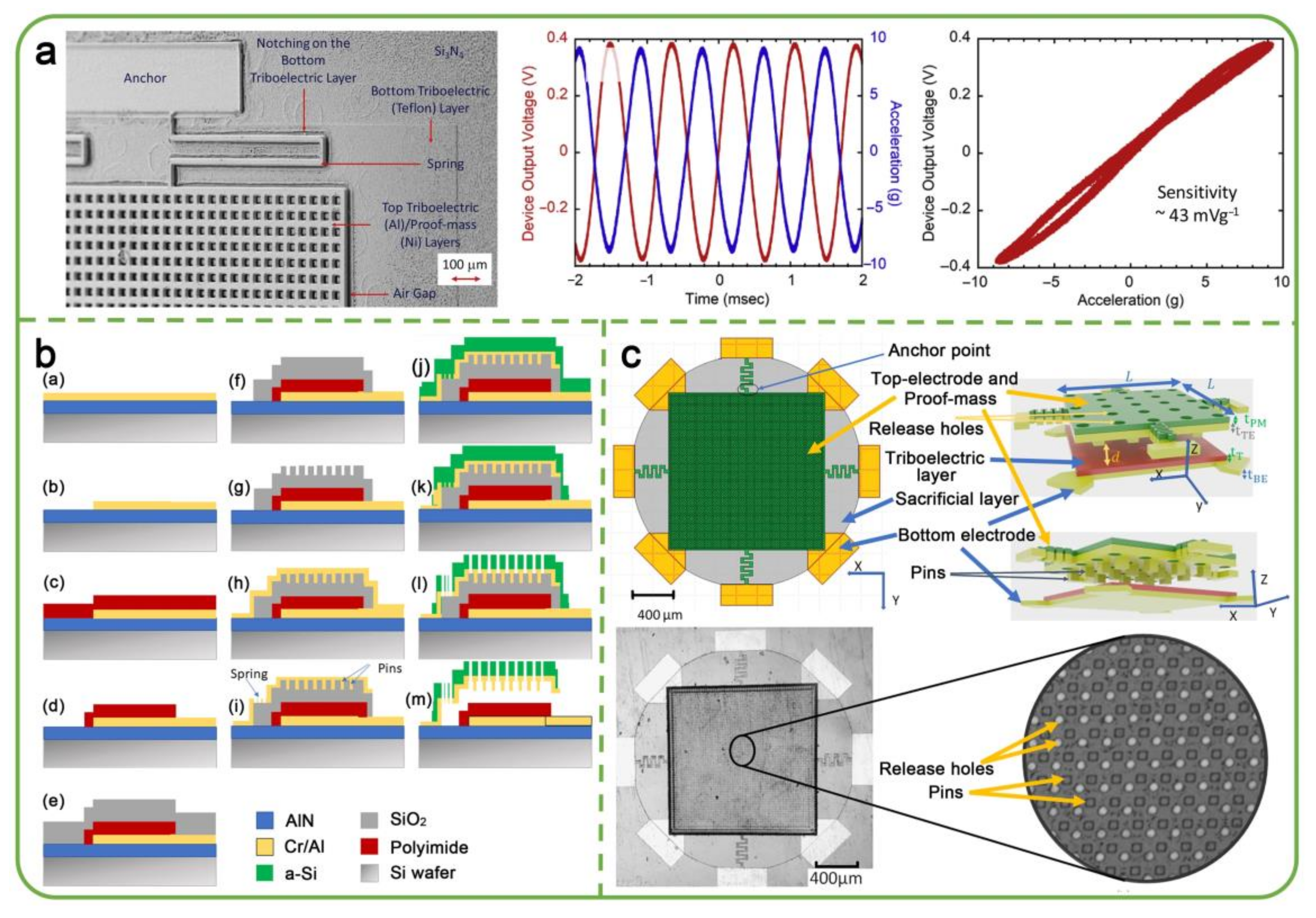
4.2. MEMS Vibration Sensors

The output performance of TENG is also a key factor restricting its application in micro-electronics. To obtain ideal output performance, the selection of triboelectric materials is crucial. According to the triboelectric series reported by Zou et al. [127], silicon is not an ideal material for obtaining high-output performance. In addition, the development of flexible TENGs through MEMS fabrication technology can further expand the application of TENGs in microelectronics. Polymers such as PDMS, PVDF, PTFE, PI and nylon are commonly used as triboelectric materials, which have a high surface charge density when contact electrification occurs. These materials can be utilized to fabricate MEMS-TENGs by surface micromachining. Hamid et al. [128] reported a novel optimization design method for low-mass and small MEMS scale (5 mm × 3 mm × 8.5 μm) TENG (MEMS-TENG). MEMS-TENG is composed of Al and PTFE to harvest high-frequency mechanical vibration energy. The device structure was dynamically optimized through the geometric model to maximize power density and output power. The simulation results show that under the conditions of an operating frequency of 800 Hz and an acceleration of 9.8 ms−2, the average power, volume, and surface average power densities generated by the device are 196.91 nW, 1544.4 W/m3, and 13.1 mW/m2, respectively. On this basis, a MEMS-TENG (5 mm × 3 mm × 15.1 μm) and sensor with high vibration frequency and wide frequency were fabricated by UV-LIGA [129]. First, the Al layer was sputtered on the Si3N4 insulation layer deposited on the surface of the silicon wafer as the bottom electrode, and then PTFE was coated to prepare the bottom triboelectric layer. Subsequently, MEMS-TENG was obtained through a series of processes, such as RIE, photolithography and electroplating. MEMS-TENG has a wide working-frequency bandwidth of 920 Hz and a sensitivity of 43 mV/g as an accelerometer, as depicted in Figure 12a. In addition, a smaller MEMS-TENG (1.5 mm × 1.5 mm × 1.1 μm) was developed by Alzgool et al. [130], and its fabrication process is displayed in Figure 12b. Aluminum nitride (AlN) as an etch stop layer was first deposited on the silicon wafer, and then through a series of steps such as sputtering, photolithography, etching, spin coating and deposition, MEMS-TENG, as shown in Figure 12c, was finally obtained. Under the condition of external shock, the Al microplate suspended in MEMS-TENG was impacted on the PI, and the contact electrification occurred, with a positive charge on Al and a negative charge on the PI. MEMS-TENG was connected to a cantilever MEMS switch, and the voltage generated by MEMS-TENG was combined with a bias DC voltage to drive a MEMS switch. MEMS-TENG was used for zero-power detection with a detection range of 1.8 to 2.4 g and a sensitivity of 1.5 V/g at a frequency of 12 kHz. The above reports on MEMS-TENGs promote the application of non-silicon materials in TENG devices.
The structural parameters and output performance of different TENGs are shown in Table 1. Compared with other TENGs, the output performance of MEMS-TENGs is lower. For MEMS-TENGs, their size is much smaller than other TENGs. In addition, the compatibility between the triboelectric materials and MEMS fabrication technology restricts the selection of materials for MEMS-TENGs, which is also an important factor. As shown in Table 1, different micro-nano manufacturing technologies have different characteristics and advantages. The output performance of MEMS-TENGs can be improved by optimizing the thickness of the triboelectric layers, and triboelectric materials through technologies such as PVD, CVD, ECD and electrospinning. Moreover, micro-nano structures can be fabricated on the surface of the triboelectric layers by laser ablation, ICP, nanoimprint and other technologies to improve the output performance of MEMS-TENGs. These technologies are conducive to the further development and application of high-performance MEMS-TENGs.

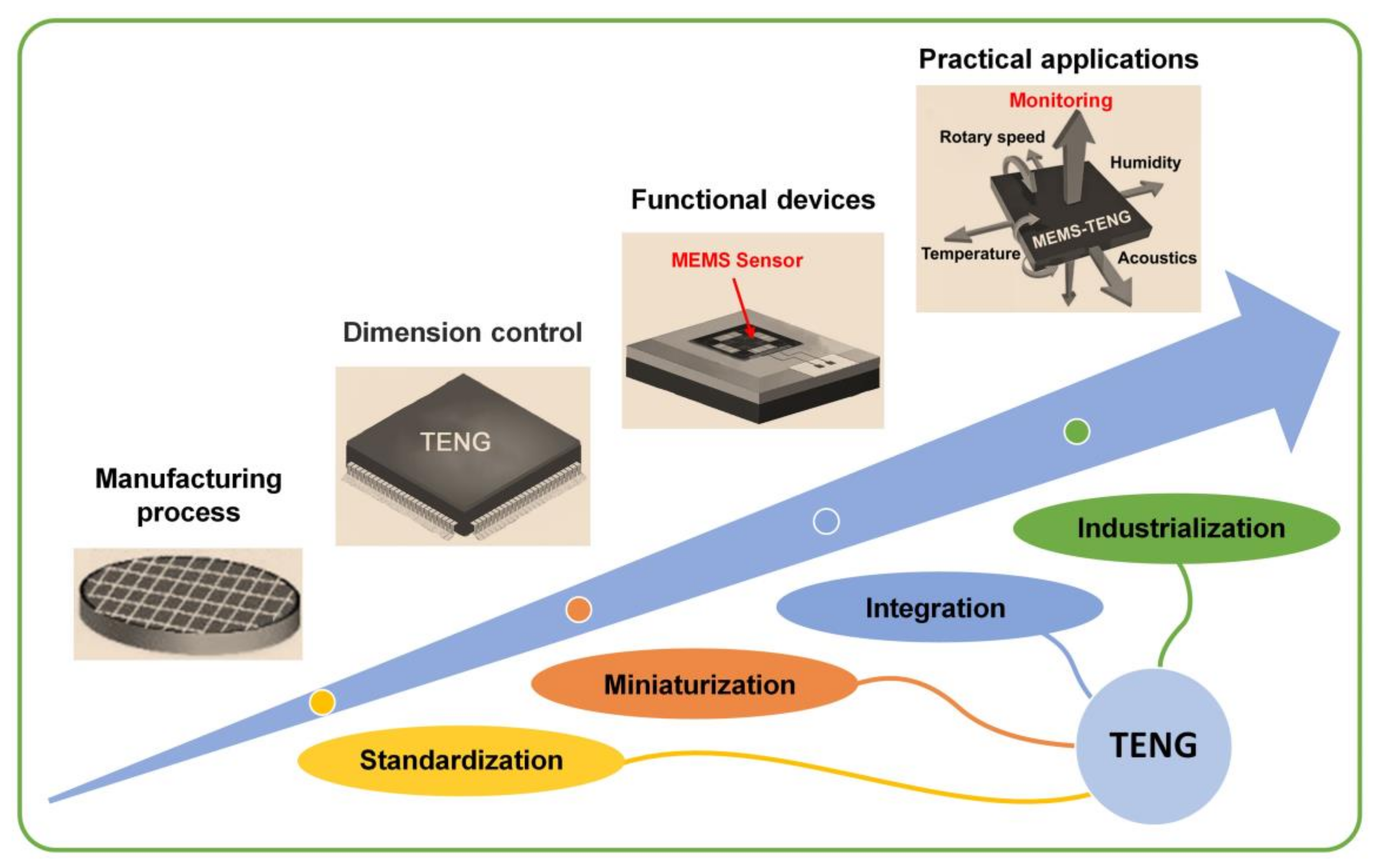
5. Conclusions and Perspectives

This review systematically summarizes the advanced micro-nano manufacturing technologies for TENGs, including the film preparation for triboelectric layers, surface processing for micro-nano structures and MEMS fabrication for TENG devices. First, CVD, PVD, ECD, electrospinning and screen printing can be used to prepare triboelectric layers, in which PVD, CVD and ECD can deposit films on different shapes and patterned substrates and can precisely control the thickness of the films. The triboelectric layers with surface micro-nano structures can be prepared by ECD and electrospinning without further processing. The surface micro-nano structures of the films can be controlled by adjusting the experimental parameters. Screen printing can produce a triboelectric layer on a large scale. Secondly, the micro-nano structures of the triboelectric layers are fabricated by soft lithography, laser ablation, ICP and nanoimprint. In the surface processing of the triboelectric layer, various micro-nano structures can be obtained by photolithography, etching and replication. Laser ablation and ICP can directly treat the surface of the triboelectric layer to create micro-nano structures, which can be adjusted by experimental parameters. In addition, nanoimprint can create a specific pattern on the surface of the triboelectric layer by designing the structure of the nanostamp. These micro-nano manufacturing technologies can further improve the output performance of TENGs. Finally, MEMS fabrication incorporates various technologies such as the photolithography, PVD, CVD, ECD and ICP, to fabricate MEMS-TENGs, which can effectively control the structures of the TENGs at micro-nano scales, for example, the μTUD cavity depth. These technologies facilitate the miniaturization, integration and standardized manufacturing of TENGs, thereby promoting the application of TENGs in microelectronics (Figure 13).
Although the advanced micro-nano manufacturing technologies for TENGs have made great progress, the selection of materials and the fabrication of micro-nano structures are facing significant challenges in the TENG manufacturing process. The following are the challenges of the advanced micro-nano manufacturing technologies for TENGs, as well as the prospects for future work.
(i) Precise control of the thickness of the triboelectric layer is of great significance for the manufacturing of ultra-thin TENGs and MEMS-TENGs. However, PVD, CVD and ECD are greatly limited in the choice of triboelectric polymers, especially those polymer materials with excellent performance, such as PDMS, nylon and PVDF. These polymers require spin coating, electrospinning, screen printing and other methods to prepare the triboelectric layers. Although electrospinning can directly prepare triboelectric layers with surface micro-nano structures, the efficiency is low. Moreover, screen printing can produce triboelectric layers on a large scale, but it is not conducive to controlling the thickness of the triboelectric layers. Thus, the fabrication of triboelectric polymer films throughPVD, CVD and ECD needs further exploration. For instance, PI film can be prepared via CVD.
(ii) In terms of the fabrication of surface micro-nano structures, soft lithography and nanoimprint need to ensure that the mold does not interact with the triboelectric material in the process of fabricating surface micro-nano structures to avoid damage to the micro-nano structures on the surface of the triboelectric layer during the demolding process. Meanwhile, the mold is easy to contaminate and has a short lifetime. These shortcomings limit some triboelectric materials from fabricating micro-nano structures by these two methods. Coating the mold with a specific material to eliminate the interaction between the mold and the triboelectric material or to develop a suitable mold is a feasible solution. Furthermore, triboelectric materials directly used in photolithography need to be further explored. Laser ablation can directly create micro-nano structures on the surface of polymers or even metal triboelectric layers, but this technology is not conducive to large-scale manufacturing. ICP can also produce micro-nano structures on the surface of the triboelectric layer, but further design of the mask is needed to produce the desired pattern. Therefore, further exploration to reduce mold contamination and prolong service life is a solution for efficient and large-scale fabrication of surface micro-nano structures.
(iii) Although the silicon-based MEMS fabrication technology is very mature, AC-TENGs with silicon as the triboelectric layer does not have obvious advantages in terms of output performance. Therefore, exploring non-silicon materials to fabricate the TENGs using MEMS fabrication technology would be beneficial for enhancing the output performance of MEMS-TENGs. Non-silicon materials include metals, oxides, polymers, carbon-based materials and composites, which make the MEMS fabrication technology have more choices for triboelectric materials. However, the compatibility between triboelectric materials and MEMS fabrication technology is a noteworthy issue when designing MEMS-TENGs. With the development of DC-TENGs, triboelectric materials, such as metals, polymers, silicon, gallium nitride, etc., can be used to fabricate MEMS-DC-TENGs through MEMS fabrication technology. Furthermore, designing MEMS-TENGs with broadband frequency characteristics is an important factor in broadening its applications. In the application of MEMS-TENGs, power management also needs further research.
In conclusion, although there are still some challenges for advanced micro-nano manufacturing technologies of TENGs, it would be further improved with the development of multi-disciplines such as materials science, microelectronics, physics and chemistry. Advanced micro-nano manufacturing technologies are highly expected to realize the standardized manufacturing of TENGs.

Author Contributions

Conceptualization, C.Z. and X.H.; writing—original draft preparation, X.H. and Y.Q.; writing—review and editing, T.B., X.L., G.L., B.F., J.Z. and C.Z.; visualization, X.H., Y.Q., T.B., X.L., B.F. and J.Z.; supervision, C.Z.; project administration, C.Z.; All authors have read and agreed to the published version of the manuscript.

Funding

This work was supported by the National Natural Science Foundation of China (No. 51922023, 61874011) and Fundamental Research Funds for the Central Universities (E1EG6804).

Conflicts of Interest

The authors declare no conflict of interest.

References

  1. Wang, Z.L. Entropy theory of distributed energy for internet of things. Nano Energy 2019, 58, 669–672. [Google Scholar] [CrossRef]
  2. Kim, W.-G.; Kim, D.-W.; Tcho, I.-W.; Kim, J.-K.; Kim, M.-S.; Choi, Y.-K. Triboelectric Nanogenerator: Structure, Mechanism, and Applications. ACS Nano 2021, 15, 258–287. [Google Scholar] [CrossRef] [PubMed]
  3. Wang, Z.L.; Chen, J.; Lin, L. Progress in triboelectric nanogenerators as a new energy technology and self-powered sensors. Energy Environ. Sci. 2015, 8, 2250–2282. [Google Scholar] [CrossRef]
  4. Luo, J.; Wang, Z.L. Recent progress of triboelectric nanogenerators: From fundamental theory to practical applications. EcoMat 2020, 2, e12059. [Google Scholar] [CrossRef]
  5. Fan, F.-R.; Tian, Z.-Q.; Wang, Z.L. Flexible triboelectric generator. Nano Energy 2012, 1, 328–334. [Google Scholar] [CrossRef]
  6. Liang, X.; Jiang, T.; Liu, G.; Feng, Y.; Zhang, C.; Wang, Z.L. Spherical triboelectric nanogenerator integrated with power management module for harvesting multidirectional water wave energy. Energy Environ. Sci. 2019, 13, 277–285. [Google Scholar] [CrossRef]
  7. Chen, H.; Lu, Q.; Cao, X.; Wang, N.; Wang, Z.L. Natural polymers based triboelectric nanogenerator for harvesting biomechanical energy and monitoring human motion. Nano Res. 2021, 15, 2505–2511. [Google Scholar] [CrossRef]
  8. Zhao, H.; Xiao, X.; Xu, P.; Zhao, T.; Song, L.; Pan, X.; Mi, J.; Xu, M.; Wang, Z.L. Dual-Tube Helmholtz Resonator-Based Triboelectric Nanogenerator for Highly Efficient Harvesting of Acoustic Energy. Adv. Energy Mater. 2019, 9, 1902824. [Google Scholar] [CrossRef]
  9. Feng, Y.; Zhang, L.; Zheng, Y.; Wang, D.; Zhou, F.; Liu, W. Leaves based triboelectric nanogenerator (TENG) and TENG tree for wind energy harvesting. Nano Energy 2019, 55, 260–268. [Google Scholar] [CrossRef]
  10. Zhang, Q.; Jiang, C.; Li, X.; Dai, S.; Ying, Y.; Ping, J. Highly Efficient Raindrop Energy-Based Triboelectric Nanogenerator for Self-Powered Intelligent Greenhouse. ACS Nano 2021, 15, 12314–12323. [Google Scholar] [CrossRef]
  11. Zi, Y.; Guo, H.; Wen, Z.; Yeh, M.-H.; Hu, C.; Wang, Z.L. Harvesting Low-Frequency (<5 Hz) Irregular Mechanical Energy: A Possible Killer Application of Triboelectric Nanogenerator. ACS Nano 2016, 10, 4797–4805. [Google Scholar] [CrossRef]
  12. Xu, J.; Zou, Y.; Nashalian, A.; Chen, J. Leverage Surface Chemistry for High-Performance Triboelectric Nanogenerators. Front. Chem. 2020, 8, 577327. [Google Scholar] [CrossRef]
  13. Wang, Y.; Liu, X.; Wang, Y.; Wang, H.; Wang, H.; Zhang, S.L.; Zhao, T.; Xu, M.; Wang, Z.L. Flexible seaweed-like triboelectric nanogenerator as a wave energy harvester powering marine internet of things. ACS Nano 2021, 15, 15700–15709. [Google Scholar] [CrossRef]
  14. Fu, X.; Xu, S.; Gao, Y.; Zhang, X.; Liu, G.; Zhou, H.; Lv, Y.; Zhang, C.; Wang, Z.L. Breeze-Wind-Energy-Powered Autonomous Wireless Anemometer Based on Rolling Contact-Electrification. ACS Energy Lett. 2021, 6, 2343–2350. [Google Scholar] [CrossRef]
  15. Xu, C.; Fu, X.; Li, C.; Liu, G.; Gao, Y.; Qi, Y.; Bu, T.; Chen, Y.; Wang, Z.L.; Zhang, C. Raindrop energy-powered autonomous wireless hyetometer based on liquid–solid contact electrification. Microsystems Nanoeng. 2022, 8, 30. [Google Scholar] [CrossRef] [PubMed]
  16. Li, Y.; Zheng, W.; Zhang, H.; Wang, H.; Cai, H.; Zhang, Y.; Yang, Z. Electron transfer mechanism of graphene/Cu heterostructure for improving the stability of triboelectric nanogenerators. Nano Energy 2020, 70, 104540. [Google Scholar] [CrossRef]
  17. Fan, B.; Liu, G.; Fu, X.; Wang, Z.; Zhang, Z.; Zhang, C. Composite film with hollow hierarchical silica/perfluoropolyether filler and surface etching for performance enhanced triboelectric nanogenerators. Chem. Eng. J. 2022, 446, 137263. [Google Scholar] [CrossRef]
  18. Varghese, H.; Chandran, A. A facile mechanical energy harvester based on spring assisted triboelectric nanogenerators. Sustain. Energy Fuels 2021, 5, 5287–5294. [Google Scholar] [CrossRef]
  19. Liu, D.; Liu, J.; Yang, M.; Cui, N.; Wang, H.; Gu, L.; Wang, L.; Qin, Y. Performance enhanced triboelectric nanogenerator by taking advantage of water in humid environments. Nano Energy 2021, 88, 106303. [Google Scholar] [CrossRef]
  20. Kim, S.; Gupta, M.K.; Lee, K.Y.; Sohn, A.; Kim, T.Y.; Shin, K.-S.; Kim, D.; Kim, S.K.; Lee, K.H.; Shin, H.-J.; et al. Transparent flexible graphene triboelectric nanogenerators. Adv. Mater. 2014, 26, 3918–3925. [Google Scholar] [CrossRef] [PubMed]
  21. Zhang, M.; Xia, L.; Dang, S.; Shi, L.; Cao, A.; Du, C. Self-powered flexible pressure sensors based on nanopatterned polymer films. Sens. Rev. 2020, 40, 629–635. [Google Scholar] [CrossRef]
  22. Chen, C.; Wen, Z.; Shi, J.; Jian, X.; Li, P.; Yeow, J.T.W.; Sun, X. Micro triboelectric ultrasonic device for acoustic energy transfer and signal communication. Nat. Commun. 2020, 11, 1–9. [Google Scholar] [CrossRef] [PubMed]
  23. Abegunde, O.O.; Akinlabi, E.T.; Oladijo, O.P.; Akinlabi, S.; Ude, A.U. Overview of thin film deposition techniques. AIMS Mater. Sci. 2019, 6, 174–199. [Google Scholar] [CrossRef]
  24. Fan, X.; Chen, J.; Yang, J.; Bai, P.; Li, Z.; Wang, Z.L. Ultrathin, Rollable, Paper-Based Triboelectric Nanogenerator for Acoustic Energy Harvesting and Self-Powered Sound Recording. ACS Nano 2015, 9, 4236–4243. [Google Scholar] [CrossRef]
  25. Yang, W.; Chen, J.; Jing, Q.; Yang, J.; Wen, X.; Su, Y.; Zhu, G.; Bai, P.; Wang, Z.L. 3D Stack Integrated Triboelectric Nanogenerator for Harvesting Vibration Energy. Adv. Funct. Mater. 2014, 24, 4090–4096. [Google Scholar] [CrossRef]
  26. Su, Y.; Wen, X.; Zhu, G.; Yang, J.; Chen, J.; Bai, P.; Wu, Z.; Jiang, Y.; Wang, Z.L. Hybrid triboelectric nanogenerator for harvesting water wave energy and as a self-powered distress signal emitter. Nano Energy 2014, 9, 186–195. [Google Scholar] [CrossRef] [Green Version]
  27. Lee, K.Y.; Yoon, H.-J.; Jiang, T.; Wen, X.; Seung, W.; Kim, S.-W.; Wang, Z.L. Fully packaged self-powered triboelectric pressure sensor using hemispheres-array. Adv. Energy Mater. 2016, 6, 1502566. [Google Scholar] [CrossRef]
  28. Zhang, W.; Diao, D.; Sun, K.; Fan, X.; Wang, P. Study on friction-electrification coupling in sliding-mode triboelectric nanogenerator. Nano Energy 2018, 48, 456–463. [Google Scholar] [CrossRef]
  29. Parajuli, P.; Sharma, B.; Behlow, H.; Rao, A.M. Fullerene-Enhanced Triboelectric Nanogenerators. Adv. Mater. Technol. 2020, 5, 2000295. [Google Scholar] [CrossRef]
  30. Xu, C.; Liu, Y.; Liu, Y.; Zheng, Y.; Feng, Y.; Wang, B.; Kong, X.; Zhang, X.; Wang, D. New inorganic coating-based triboelectric nanogenerators with anti-wear and self-healing properties for efficient wave energy harvesting. Appl. Mater. Today 2020, 20, 100645. [Google Scholar] [CrossRef]
  31. Jones, A.C.; Hitchman, M.L. Overview of chemical vapour deposition. In Chemical Vapour Deposition: Precursors, Processes and Applications; Royal Society of Chemistry: London, UK, 2009; Chapter 1; pp. 1–36. [Google Scholar] [CrossRef] [Green Version]
  32. Carlsson, J.-O.; Martin, M.P. Handbook of deposition technologies for films and coatings (Third Edition). Sci. Appl. Technol. 2010, 314–363. [Google Scholar] [CrossRef]
  33. Chandrashekar, B.N.; Deng, B.; Smitha, A.S.; Chen, Y.; Tan, C.; Zhang, H.; Peng, H.; Liu, Z. Roll-to-Roll Green Transfer of CVD Graphene onto Plastic for a Transparent and Flexible Triboelectric Nanogenerator. Adv. Mater. 2015, 27, 5210–5216. [Google Scholar] [CrossRef]
  34. Shankaregowda, S.A.; Nanjegowda, C.B.; Cheng, X.-L.; Shi, M.-Y.; Liu, Z.-F.; Zhang, H.-X. A flexible and transparent graphene-based triboelectric nanogenerator. IEEE Trans Nanotechnol. 2016, 15, 435–441. [Google Scholar] [CrossRef]
  35. Khan, S.A.; Zhang, H.L.; Xie, Y.; Gao, M.; Shah, M.A.; Qadir, A.; Lin, Y. Flexible Triboelectric Nanogenerator Based on Carbon Nanotubes for Self-Powered Weighing. Adv. Eng. Mater. 2016, 19, 1600710. [Google Scholar] [CrossRef]
  36. Kim, M.; Kim, S.H.; Park, M.U.; Lee, C.; Kim, M.; Yi, Y.; Yoo, K.-H. MoS2 triboelectric nanogenerators based on depletion layers. Nano Energy 2019, 65, 104079. [Google Scholar] [CrossRef]
  37. Liu, Z.; Zhao, Z.; Zeng, X.; Fu, X.; Hu, Y. Ultrathin, flexible and transparent graphene-based triboelectric nanogenerators for attachable curvature monitoring. J. Phys. D Appl. Phys. 2019, 52, 314002. [Google Scholar] [CrossRef]
  38. Chen, P.-J.; Rodger, D.C.; Meng, E.; Hwnmayun, M.S.; Tail, Y.-C. Implantable unpowered parylene MEMS intraocular pressure sensor. In Proceedings of the 206 International Conference on Microtechnologies in Medicine and Biology, Okinawa, Japan, 9–12 May 2006; pp. 256–259. [Google Scholar] [CrossRef] [Green Version]
  39. Li, P.-Y.; Givrad, T.K.; Holschneider, D.P.; Maarek, J.-M.I.; Meng, E. A Parylene MEMS Electrothermal Valve. J. Microelectromech. Syst. 2009, 18, 1184–1197. [Google Scholar] [CrossRef] [Green Version]
  40. Kim, J.Y.-H.; Liu, Y.; Scianmarello, N.; Tai, Y.C. Piezoelectric parylene-C MEMS microphone. In Proceedings of the 2013 Transducers & Eurosensors XXVII: The 17th International Conference on Solid-State Sensors, Actuators and Microsystems (TRANSDUCERS & EUROSENSORS XXVII), Barcelona, Spain, 16–20 October 2013; pp. 39–42. [Google Scholar] [CrossRef]
  41. Kim, B.J.; Gutierrez, C.A.; Meng, E. Parylene-Based Electrochemical-MEMS Force Sensor for Studies of Intracortical Probe Insertion Mechanics. J. Microelectromech. Syst. 2015, 24, 1534–1544. [Google Scholar] [CrossRef]
  42. Wu, C.-H.; Kang, D.; Chen, P.-H.; Tai, Y.-C. MEMS thermal flow sensors. Sensors Actuators A Phys. 2016, 241, 135–144. [Google Scholar] [CrossRef]
  43. Ortigoza-Diaz, J.; Scholten, K.; Larson, C.; Cobo, A.; Hudson, T.; Yoo, J.; Baldwin, A.; Hirschberg, A.W.; Meng, E. Techniques and Considerations in the Microfabrication of Parylene C Microelectromechanical Systems. Micromachines 2018, 9, 422. [Google Scholar] [CrossRef] [PubMed] [Green Version]
  44. Mariello, M.; Scarpa, E.; Algieri, L.; Guido, F.; Mastronardi, V.M.; Qualtieri, A.; De Vittorio, M. Novel Flexible Triboelectric Nanogenerator based on Metallized Porous PDMS and Parylene C. Energies 2020, 13, 1625. [Google Scholar] [CrossRef] [Green Version]
  45. Wang, Q.; Xue, Q.; Chen, T.; Li, J.; Liu, Y.; Shan, X.; Liu, F.; Jia, J. Recent advances in electrochemical sensors for antibiotics and their applications. Chin. Chem. Lett. 2020, 32, 609–619. [Google Scholar] [CrossRef]
  46. Ko, Y.H.; Nagaraju, G.; Lee, S.H.; Yu, J.S. PDMS-based Triboelectric and Transparent Nanogenerators with ZnO Nanorod Arrays. ACS Appl. Mater. Interfaces 2014, 6, 6631–6637. [Google Scholar] [CrossRef] [PubMed]
  47. Zhang, H.; Zhang, P.; Deng, L.; Zhang, W.; Liu, B.; Ren, D.; Yang, Z. Three-Dimensional Polypyrrole Nanoarrays for Wearable Triboelectric Nanogenerators. ACS Appl. Nano Mater. 2022, 5, 11219–11228. [Google Scholar] [CrossRef]
  48. Meng, Y.; Zhang, L.; Xu, G.; Wang, H. Direct-current generators based on conductive polymers for self-powered flexible devices. Sci. Rep. 2021, 11, 1–10. [Google Scholar] [CrossRef]
  49. Mariappan, V.K.; Krishnamoorthy, K.; Pazhamalai, P.; Natarajan, S.; Sahoo, S.; Nardekar, S.S.; Kim, S.-J. Antimonene dendritic nanostructures: Dual-functional material for high-performance energy storage and harvesting devices. Nano Energy 2020, 77, 105248. [Google Scholar] [CrossRef]
  50. Yang, G.; Yang, H.; Wang, M.; Sun, Y.; Wang, M. Application of Nanofiber Material Based on Electrospinning Technology in Sports Rehabilitation of Basketball Player’s Wrist Joint. J. Nanomater. 2022, 2022, 1–9. [Google Scholar] [CrossRef]
  51. Xue, J.; Wu, T.; Dai, Y.; Xia, Y. Electrospinning and Electrospun Nanofibers: Methods, Materials, and Applications. Chem. Rev. 2019, 119, 5298–5415. [Google Scholar] [CrossRef]
  52. Lu, T.; Cui, J.; Qu, Q.; Wang, Y.; Zhang, J.; Xiong, R.; Ma, W.; Huang, C. Multistructured Electrospun Nanofibers for Air Filtration: A Review. ACS Appl. Mater. Interfaces 2021, 13, 23293–23313. [Google Scholar] [CrossRef]
  53. Huang, T.; Wang, C.; Yu, H.; Wang, H.; Zhang, Q.; Zhu, M. Human walking-driven wearable all-fiber triboelectric nanogenerator containing electrospun polyvinylidene fluoride piezoelectric nanofibers. Nano Energy 2014, 14, 226–235. [Google Scholar] [CrossRef]
  54. Zhao, S.; Wang, J.; Du, X.; Wang, J.; Cao, R.; Yin, Y.; Zhang, X.; Yuan, Z.; Xing, Y.; Pui, D.Y.H.; et al. All-Nanofiber-Based Ultralight Stretchable Triboelectric Nanogenerator for Self-Powered Wearable Electronics. ACS Appl. Energy Mater. 2018, 1, 2326–2332. [Google Scholar] [CrossRef]
  55. Ye, Q.; Wu, Y.; Qi, Y.; Shi, L.; Huang, S.; Zhang, L.; Li, M.; Li, W.; Zeng, X.; Wo, H.; et al. Effects of liquid metal particles on performance of triboelectric nanogenerator with electrospun polyacrylonitrile fiber films. Nano Energy 2019, 61, 381–388. [Google Scholar] [CrossRef]
  56. Li, Y.; Xiong, J.; Lv, J.; Chen, J.; Gao, D.; Zhang, X.; Lee, P.S. Mechanically interlocked stretchable nanofibers for multifunctional wearable triboelectric nanogenerator. Nano Energy 2020, 78, 105358. [Google Scholar] [CrossRef]
  57. Shi, L.; Jin, H.; Dong, S.; Huang, S.; Kuang, H.; Xu, H.; Chen, J.; Xuan, W.; Zhang, S.; Li, S.; et al. High-performance triboelectric nanogenerator based on electrospun PVDF-graphene nanosheet composite nanofibers for energy harvesting. Nano Energy 2020, 80, 105599. [Google Scholar] [CrossRef]
  58. Sun, N.; Wang, G.-G.; Zhao, H.-X.; Cai, Y.-W.; Li, J.-Z.; Li, G.-Z.; Zhang, X.-N.; Wang, B.-L.; Han, J.-C.; Wang, Y.; et al. Waterproof, breathable and washable triboelectric nanogenerator based on electrospun nanofiber films for wearable electronics. Nano Energy 2021, 90, 106639. [Google Scholar] [CrossRef]
  59. Gu, G.Q.; Han, C.B.; Lu, C.X.; He, C.; Jiang, T.; Gao, Z.L.; Li, C.J.; Wang, Z.L. Triboelectric Nanogenerator Enhanced Nanofiber Air Filters for Efficient Particulate Matter Removal. ACS Nano 2017, 11, 6211–6217. [Google Scholar] [CrossRef] [PubMed]
  60. Xiong, J.; Luo, H.; Gao, D.; Zhou, X.; Cui, P.; Thangavel, G.; Parida, K.; Lee, P.S. Self-restoring, waterproof, tunable microstructural shape memory triboelectric nanogenerator for self-powered water temperature sensor. Nano Energy 2019, 61, 584–593. [Google Scholar] [CrossRef]
  61. Jang, S.; Kim, H.; Kim, Y.; Kang, B.J.; Oh, J.H. Honeycomb-like nanofiber based triboelectric nanogenerator using self-assembled electrospun poly(vinylidene fluoride-co-trifluoroethylene) nanofibers. Appl. Phys. Lett. 2016, 108, 143901. [Google Scholar] [CrossRef]
  62. Huang, J.; Hao, Y.; Zhao, M.; Li, W.; Huang, F.; Wei, Q. All-Fiber-Structured Triboelectric Nanogenerator via One-Pot Electrospinning for Self-Powered Wearable Sensors. ACS Appl. Mater. Interfaces 2021, 13, 24774–24784. [Google Scholar] [CrossRef] [PubMed]
  63. Hao, Y.; Huang, J.; Liao, S.; Chen, D.; Wei, Q. All-electrospun performance-enhanced triboelectric nanogenerator based on the charge-storage process. J. Mater. Sci. 2022, 57, 5334–5345. [Google Scholar] [CrossRef]
  64. Huang, T.; Lu, M.; Yu, H.; Zhang, Q.; Wang, H.; Zhu, M. Enhanced Power Output of a Triboelectric Nanogenerator Composed of Electrospun Nanofiber Mats Doped with Graphene Oxide. Sci. Rep. 2015, 5, srep13942. [Google Scholar] [CrossRef] [Green Version]
  65. Huang, T.; Yu, H.; Wang, H.; Zhang, Q.; Zhu, M. Hydrophobic SiO2 Electret Enhances the Performance of Poly(vinylidene fluoride) Nanofiber-Based Triboelectric Nanogenerator. J. Phys. Chem. C 2016, 120, 26600–26608. [Google Scholar] [CrossRef]
  66. Ozen, A.; Ozel, F.; Kınas, Z.; Karabiber, A.; Polat, S. Spring assisted triboelectric nanogenerator based on sepiolite doped polyacrylonitrile nanofibers. Sustain. Energy Technol. Assessments 2021, 47, 101492. [Google Scholar] [CrossRef]
  67. Jiang, C.; Wu, C.; Li, X.; Yao, Y.; Lan, L.; Zhao, F.; Ye, Z.; Ying, Y.; Ping, J. All-electrospun flexible triboelectric nanogenerator based on metallic MXene nanosheets. Nano Energy 2019, 59, 268–276. [Google Scholar] [CrossRef]
  68. Chu, Z.; Peng, J.; Jin, W. Advanced nanomaterial inks for screen-printed chemical sensors. Sens. Actuators B Chem. 2017, 243, 919–926. [Google Scholar] [CrossRef]
  69. Gong, X.; Huang, K.; Wu, Y.-H.; Zhang, X.-S. Recent progress on screen-printed flexible sensors for human health monitoring. Sensors Actuators A Phys. 2022, 345, 113821. [Google Scholar] [CrossRef]
  70. Zhang, Y.; Zhu, Y.; Zheng, S.; Zhang, L.; Shi, X.; He, J.; Chou, X.; Wu, Z.-S. Ink formulation, scalable applications and challenging perspectives of screen printing for emerging printed microelectronics. J. Energy Chem. 2021, 63, 498–513. [Google Scholar] [CrossRef]
  71. Cao, R.; Wang, J.; Zhao, S.; Yang, W.; Yuan, Z.; Yin, Y.; Du, X.; Li, N.-W.; Zhang, X.; Li, X.; et al. Self-powered nanofiber-based screen-print triboelectric sensors for respiratory monitoring. Nano Res. 2018, 11, 3771–3779. [Google Scholar] [CrossRef]
  72. Sagar, H.P.; Meti, S.; Bhat, U.K.; Gupta, D. Triboelectric effect based self-powered compact vibration sensor for predictive maintenance of industrial machineries. Meas. Sci. Technol. 2021, 32, 095119. [Google Scholar] [CrossRef]
  73. Meti, S.; Sagar, H.P.; Rahman, M.R.; Bhat, K.U. Assessment of triboelectricity in colossal-surface-area-lanthanum oxide nanocrystals synthesized via low-temperature hydrothermal process. J. Mater. Sci. Mater. Electron. 2021, 32, 20351–20361. [Google Scholar] [CrossRef]
  74. Paosangthong, W.; Wagih, M.; Torah, R.; Beeby, S. Textile-based triboelectric nanogenerator with alternating positive and negative freestanding grating structure. Nano Energy 2019, 66, 104148. [Google Scholar] [CrossRef]
  75. Liu, H.; Xu, Y.; Xiao, Y.; Zhang, S.; Qu, C.; Lv, L.; Chen, H.; Song, G. Highly Adaptive Liquid–Solid Triboelectric Nanogenerator-Assisted Self-Powered Water Wave Motion Sensor. ACS Appl. Electron. Mater. 2022, 4, 3870–3879. [Google Scholar] [CrossRef]
  76. Prutvi, S.H.; Korrapati, M.; Gupta, D. Self-powering vibration sensor based on a cantilever system with a single-electrode mode triboelectric nanogenerator. Meas. Sci. Technol. 2022, 33, 075115. [Google Scholar] [CrossRef]
  77. Yang, H.J.; Lee, J.-W.; Seo, S.H.; Jeong, B.; Lee, B.; Do, W.J.; Kim, J.H.; Cho, J.Y.; Jo, A.; Jeong, H.J.; et al. Fully stretchable self-charging power unit with micro-supercapacitor and triboelectric nanogenerator based on oxidized single-walled carbon nanotube/polymer electrodes. Nano Energy 2021, 86, 106083. [Google Scholar] [CrossRef]
  78. Scharnweber, T.; Truckenmüller, R.; Schneider, A.M.; Welle, A.; Reinhardt, M.; Giselbrecht, S. Rapid prototyping of microstructures in polydimethylsiloxane (PDMS) by direct UV-lithography. Lab Chip 2011, 11, 1368–1371. [Google Scholar] [CrossRef]
  79. Xue, C.-Y.; Zhang, W.; Choo, W.H.S.; Yang, K.-L. Simplest Method for Creating Micropatterned Nanostructures on PDMS with UV Light. Langmuir 2011, 27, 13410–13414. [Google Scholar] [CrossRef] [PubMed]
  80. Yang, W.; Wang, X.; Li, H.; Wu, J.; Hu, Y.; Li, Z.; Liu, H. Fundamental research on the effective contact area of micro-/nano-textured surface in triboelectric nanogenerator. Nano Energy 2019, 57, 41–47. [Google Scholar] [CrossRef]
  81. Fan, F.-R.; Lin, L.; Zhu, G.; Wu, W.; Zhang, R.; Wang, Z.L. Transparent Triboelectric Nanogenerators and Self-Powered Pressure Sensors Based on Micropatterned Plastic Films. Nano Lett. 2012, 12, 3109–3114. [Google Scholar] [CrossRef] [Green Version]
  82. Zhang, L.; Su, C.; Cheng, L.; Cui, N.; Gu, L.; Qin, Y.; Yang, R.; Zhou, F. Enhancing the Performance of Textile Triboelectric Nanogenerators with Oblique Microrod Arrays for Wearable Energy Harvesting. ACS Appl. Mater. Interfaces 2019, 11, 26824–26829. [Google Scholar] [CrossRef]
  83. Dhakar, L.; Tay, F.E.H.; Lee, C. Development of a Broadband Triboelectric Energy Harvester With SU-8 Micropillars. J. Microelectromech. Syst. 2014, 24, 91–99. [Google Scholar] [CrossRef]
  84. Hong, S.; Lee, H.; Yeo, J.; Ko, S.H. Digital selective laser methods for nanomaterials: From synthesis to processing. Nano Today 2016, 11, 547–564. [Google Scholar] [CrossRef]
  85. Palneedi, H.; Park, J.H.; Maurya, D.; Peddigari, M.; Hwang, G.-T.; Annapureddy, V.; Kim, J.-W.; Choi, J.-J.; Hahn, B.-D.; Priya, S.; et al. Laser irradiation of metal oxide films and nanostructures: Applications and advances. Adv. Mater. 2018, 30, 1705148. [Google Scholar] [CrossRef]
  86. Hu, H.; Li, Q.; Li, L.; Teng, X.; Feng, Z.; Zhang, Y.; Wu, M.; Qiu, J. Laser Irradiation of Electrode Materials for Energy Storage and Conversion. Matter 2020, 3, 95–126. [Google Scholar] [CrossRef]
  87. Zhao, L.; Liu, Z.; Chen, D.; Liu, F.; Yang, Z.; Li, X.; Yu, H.; Liu, H.; Zhou, W. Laser Synthesis and Microfabrication of Micro/Nanostructured Materials Toward Energy Conversion and Storage. Nano-Micro Lett. 2021, 13, 1–48. [Google Scholar] [CrossRef]
  88. Xiao, X.; Lü, C.; Wang, G.; Xu, Y.; Wang, J.; Yang, H. Flexible triboelectric nanogenerator from micro-nano structured polydimethylsiloxane. Chem. Res. Chin. Univ. 2015, 31, 434–438. [Google Scholar] [CrossRef]
  89. Kim, D.; Tcho, I.-W.; Jin, I.K.; Park, S.-J.; Jeon, S.-B.; Kim, W.-G.; Cho, H.-S.; Lee, H.-S.; Jeoung, S.C.; Choi, Y.-K. Direct-laser-patterned friction layer for the output enhancement of a triboelectric nanogenerator. Nano Energy 2017, 35, 379–386. [Google Scholar] [CrossRef]
  90. Muthu, M.; Pandey, R.; Wang, X.; Chandrasekhar, A.; Palani, I.; Singh, V. Enhancement of triboelectric nanogenerator output performance by laser 3D-Surface pattern method for energy harvesting application. Nano Energy 2020, 78, 105205. [Google Scholar] [CrossRef]
  91. Cho, H.; Jo, S.; Kim, I.; Kim, D. Film-Sponge-Coupled Triboelectric Nanogenerator with Enhanced Contact Area Based on Direct Ultraviolet Laser Ablation. ACS Appl. Mater. Interfaces 2021, 13, 48281–48291. [Google Scholar] [CrossRef]
  92. Wang, S.; Xie, G.; Tai, H.; Su, Y.; Yang, B.; Zhang, Q.; Du, X.; Jiang, Y. Ultrasensitive flexible self-powered ammonia sensor based on triboelectric nanogenerator at room temperature. Nano Energy 2018, 51, 231–240. [Google Scholar] [CrossRef]
  93. Phan, H.; Hoa, P.; Tam, H.; Thang, P. Q-switched pulsed laser direct writing of aluminum surface micro/nanostructure for triboelectric performance enhancement. J. Sci. Adv. Mater. Devices 2020, 6, 84–91. [Google Scholar] [CrossRef]
  94. Huang, J.; Fu, X.; Liu, G.; Xu, S.; Li, X.; Zhang, C.; Jiang, L. Micro/nano-structures-enhanced triboelectric nanogenerators by femtosecond laser direct writing. Nano Energy 2019, 62, 638–644. [Google Scholar] [CrossRef]
  95. Phan, H.; Hoa, P.; Tam, H.; Thang, P.; Duc, N. Multi-directional triboelectric nanogenerator based on industrial Q-switched pulsed laser etched Aluminum film. Extreme Mech. Lett. 2020, 40, 100886. [Google Scholar] [CrossRef]
  96. Chung, C.; Ke, K. High contact surface area enhanced Al/PDMS triboelectric nanogenerator using novel overlapped microneedle arrays and its application to lighting and self-powered devices. Appl. Surf. Sci. 2020, 508, 145310. [Google Scholar] [CrossRef]
  97. Pradel, K.C.; Fukata, N. Systematic optimization of triboelectric nanogenerator performance through surface micropatterning. Nano Energy 2021, 83, 105856. [Google Scholar] [CrossRef]
  98. Zhang, H.; Cui, X.; Cao, S.; Zhang, Q.; Sang, S.; Zhang, W. Human Body as a Power Source for Biomechanical Energy Scavenging Based on Electrode-Free Triboelectric Nanogenerators. Energy Technol. 2018, 6, 2053–2057. [Google Scholar] [CrossRef]
  99. Chen, G.; Xu, L.; Zhang, P.; Chen, B.; Wang, G.; Ji, J.; Pu, X.; Wang, Z.L. Seawater Degradable Triboelectric Nanogenerators for Blue Energy. Adv. Mater. Technol. 2020, 5, 2000455. [Google Scholar] [CrossRef]
  100. Li, C.; Wang, Z.; Shu, S.; Tang, W. A Self-Powered Vector Angle/Displacement Sensor Based on Triboelectric Nanogenerator. Micromachines 2021, 12, 231. [Google Scholar] [CrossRef]
  101. Shin, Y.; Cho, S.; Han, S.; Jung, G.Y. Omni-directional wind-driven triboelectric nanogenerator with cross-shaped dielectric film. Nano Converg. 2021, 8, 25. [Google Scholar] [CrossRef]
  102. Prada, T.; Harnchana, V.; Lakhonchai, A.; Chingsungnoen, A.; Poolcharuansin, P.; Chanlek, N.; Klamchuen, A.; Thongbai, P.; Amornkitbamrung, V. Enhancement of output power density in a modified polytetrafluoroethylene surface using a sequential O2/Ar plasma etching for triboelectric nanogenerator applications. Nano Res. 2022, 15, 272–279. [Google Scholar] [CrossRef]
  103. Cheng, G.-G.; Jiang, S.-Y.; Li, K.; Zhang, Z.-Q.; Wang, Y.; Yuan, N.-Y.; Ding, J.-N.; Zhang, W. Effect of argon plasma treatment on the output performance of triboelectric nanogenerator. Appl. Surf. Sci. 2017, 412, 350–356. [Google Scholar] [CrossRef]
  104. Wang, M.; Li, W.; You, C.; Wang, Q.; Zeng, X.; Chen, M. Triboelectric nanogenerator based on 317L stainless steel and ethyl cellulose for biomedical applications. RSC Adv. 2017, 7, 6772–6779. [Google Scholar] [CrossRef] [Green Version]
  105. Jeon, S.-B.; Kim, S.; Park, S.-J.; Seol, M.-L.; Kim, D.; Chang, Y.K.; Choi, Y.-K. Self-powered electro-coagulation system driven by a wind energy harvesting triboelectric nanogenerator for decentralized water treatment. Nano Energy 2016, 28, 288–295. [Google Scholar] [CrossRef]
  106. Chen, S.W.; Cao, X.; Wang, N.; Ma, L.; Zhu, H.R.; Willander, M.; Jie, Y.; Wang, Z.L. An Ultrathin Flexible Single-Electrode Triboelectric-Nanogenerator for Mechanical Energy Harvesting and Instantaneous Force Sensing. Adv. Energy Mater. 2016, 7, 1601255. [Google Scholar] [CrossRef]
  107. Wang, S.; He, M.; Weng, B.; Gan, L.; Zhao, Y.; Li, N.; Xie, Y. Stretchable and Wearable Triboelectric Nanogenerator Based on Kinesio Tape for Self-Powered Human Motion Sensing. Nanomaterials 2018, 8, 657. [Google Scholar] [CrossRef] [PubMed] [Green Version]
  108. Jiang, Y.; Dong, K.; Li, X.; An, J.; Wu, D.; Peng, X.; Yi, J.; Ning, C.; Cheng, R.; Yu, P.; et al. Stretchable, washable, and ultrathin triboelectric nanogenerators as skin-like highly sensitive self-powered haptic sensors. Adv. Funct. Mater. 2020, 31, 2005584. [Google Scholar] [CrossRef]
  109. Lin, L.; Xie, Y.; Niu, S.; Wang, S.; Yang, P.-K.; Wang, Z.L. Robust Triboelectric Nanogenerator Based on Rolling Electrification and Electrostatic Induction at an Instantaneous Energy Conversion Efficiency of ∼55%. ACS Nano 2015, 9, 922–930. [Google Scholar] [CrossRef]
  110. Cheng, X.; Meng, B.; Chen, X.; Han, M.; Chen, H.; Su, Z.; Shi, M.; Zhang, H. Single-Step Fluorocarbon Plasma Treatment-Induced Wrinkle Structure for High-Performance Triboelectric Nanogenerator. Small 2015, 12, 229–236. [Google Scholar] [CrossRef]
  111. Chou, S.Y.; Krauss, P.R.; Renstrom, P.J. Imprint of sub-25 nm vias and trenches in polymers. Appl. Phys. Lett. 1995, 67, 3114–3116. [Google Scholar] [CrossRef] [Green Version]
  112. Guo, L.J. Recent progress in nanoimprint technology and its applications. J. Phys. D Appl. Phys. 2004, 37, R123–R141. [Google Scholar] [CrossRef]
  113. Guo, L.J. Nanoimprint Lithography: Methods and Material Requirements. Adv. Mater. 2007, 19, 495–513. [Google Scholar] [CrossRef] [Green Version]
  114. Yoo, D.; Lee, S.; Lee, J.-W.; Lee, K.; Go, E.Y.; Hwang, W.; Song, I.; Cho, S.B.; Kim, D.W.; Choi, D.; et al. Reliable DC voltage generation based on the enhanced performance triboelectric nanogenerator fabricated by nanoimprinting-poling process and an optimized high efficiency integrated circuit. Nano Energy 2019, 69, 104388. [Google Scholar] [CrossRef]
  115. Zhang, M.; Xia, L.; Dang, S.; Shi, L.; Cao, A.; Deng, Q.; Du, C. A flexible single-electrode-based triboelectric nanogenerator based on double-sided nanostructures. AIP Adv. 2019, 9, 075221. [Google Scholar] [CrossRef] [Green Version]
  116. Choi, D.; Yoo, D.; Kim, D.S. One-Step Fabrication of Transparent and Flexible Nanotopographical-Triboelectric Nanogenerators via Thermal Nanoimprinting of Thermoplastic Fluoropolymers. Adv. Mater. 2015, 27, 7386–7394. [Google Scholar] [CrossRef]
  117. Mahmud, M.P.; Lee, J.; Kim, G.; Lim, H.; Choi, K.-B. Improving the surface charge density of a contact-separation-based triboelectric nanogenerator by modifying the surface morphology. Microelectron. Eng. 2016, 159, 102–107. [Google Scholar] [CrossRef]
  118. Dudem, B.; Kim, D.H.; Mule, A.R.; Yu, J.S. Enhanced Performance of Microarchitectured PTFE-Based Triboelectric Nanogenerator via Simple Thermal Imprinting Lithography for Self-Powered Electronics. ACS Appl. Mater. Interfaces 2018, 10, 24181–24192. [Google Scholar] [CrossRef]
  119. Kim, J.; Kim, J.; Kim, J.; Ahn, J.; Jeong, J.; Park, I.; Kim, D.; Oh, I. Collectively Exhaustive Hybrid Triboelectric Nanogenerator Based on Flow-Induced Impacting-Sliding Cylinder for Ocean Energy Harvesting. Adv. Energy Mater. 2021, 12, 2103076. [Google Scholar] [CrossRef]
  120. La, M.; Choi, J.H.; Choi, J.-Y.; Hwang, T.Y.; Kang, J.; Choi, D. Development of the Triboelectric Nanogenerator Using a Metal-to-Metal Imprinting Process for Improved Electrical Output. Micromachines 2018, 9, 551. [Google Scholar] [CrossRef]
  121. Mishra, M.K.; Dubey, V.; Mishra, P.M.; Khan, I. MEMS Technology: A Review. J. Eng. Res. Rep. 2019, 4, 1–24. [Google Scholar] [CrossRef]
  122. Coppola, G.; Iodice, M.; Finizio, A.; De Nicola, S.M.; Pierattini, G.; Ferraro, P., Jr.; Magro, C.; Spoto, G. Digital holography microscope as tool for microelectromechanical systems characterization and design. J. Micro/Nanolithography MEMS MOEMS 2005, 4, 013012. [Google Scholar] [CrossRef]
  123. Tilli, M.; Paulasto-Krockel, M.; Petzold, M.; Theuss, H.; Motooka, T.; Lindroos, V. Handbook of Silicon Based MEMS Materials and Technologies; Elsevier: Amsterdam, The Netherlands, 2020; p. xxi. [Google Scholar]
  124. Ali, W.R.; Prasad, M. Piezoelectric MEMS based acoustic sensors: A review. Sensors Actuators A Phys. 2019, 301, 111756. [Google Scholar] [CrossRef]
  125. Prasad, M.; Sahula, V.; Khanna, V.K. Design and Fabrication of Si-Diaphragm, ZnO Piezoelectric Film-Based MEMS Acoustic Sensor Using SOI Wafers. IEEE Trans. Semicond. Manuf. 2013, 26, 233–241. [Google Scholar] [CrossRef]
  126. Ali, W.R.; Prasad, M. Fabrication of microchannel and diaphragm for a MEMS acoustic sensor using wet etching technique. Microelectron. Eng. 2021, 253, 111670. [Google Scholar] [CrossRef]
  127. Zou, H.; Zhang, Y.; Guo, L.; Wang, P.; He, X.; Dai, G.; Zheng, H.; Chen, C.; Wang, A.C.; Xu, C.; et al. Quantifying the triboelectric series. Nat. Commun. 2019, 10, 1–9. [Google Scholar] [CrossRef] [PubMed] [Green Version]
  128. Hamid, H.M.A.; Celik-Butler, Z. Design and Optimization of a MEMS Triboelectric Energy Harvester for Nano-sensor Applications. In Proceedings of the 2019 IEEE Sensors Applications Symposium (SAS), Sophia Antipolis, France, 11–13 March 2019; pp. 1–6. [Google Scholar] [CrossRef]
  129. Hamid, H.M.A.; Çelik-Butler, Z. A novel MEMS triboelectric energy harvester and sensor with a high vibrational operating frequency and wide bandwidth fabricated using UV-LIGA technique. Sensors Actuators A Phys. 2020, 313, 112175. [Google Scholar] [CrossRef]
  130. Alzgool, M.; Mousavi, M.; Davaji, B.; Towfighian, S. Micro-triboelectric generator for zero-power shock detection. Nano Energy 2022, 103, 107758. [Google Scholar] [CrossRef]
Figure 1. Advanced micro-nano manufacturing technologies for TENGs. Image of the triboelectric layer [20]. Copyright permission from Wiley-VCH. Representative image of the surface micro-nano structures [21]. Copyright permission from Emerald Publishing Limited. Representative diagram of the TENG device [22]. Copyright permission from Nature Publishing Group.
Nanoenergyadv 02 00017 g001
Figure 2. Triboelectric layers prepared by PVD. (a) Paper-based TENG with Cu was deposited on a small hole array substrate as a triboelectric layer for harvesting acoustic energy [24]. Copyright permission from ACS. (b) Al was deposited onto pinned fingers by PVD and used as a triboelectric layer for 3D-TENG [25]. Copyright permission from Wiley-VCH. (c) Cu was deposited onto the wavy-shaped Kapton film as a triboelectric layer by electron beam evaporation [26]. Copyright permission from Elsevier. (d) Structure of the H-TENG based on Cu deposition on a hemispherical PDMS array film as a positive triboelectric layer [27]. Copyright permission from Wiley-VCH. (e) Structure diagram of the TENG on the motorized pushing tester and the VOC of four different TENGs with C60 deposited on PET/ITO as a triboelectric layer [29]. Copyright permission from Wiley-VCH.
Nanoenergyadv 02 00017 g002
Figure 3. Triboelectric layers prepared by CVD. (a) Fabrication process of the roll-to-roll production of large-area graphene on copper by CVD and the roll-to-roll “green” transfer of graphene onto EVA/PET film [33]. Copyright permission from Wiley-VCH. (b) Schematic diagram of carbon nanotubes prepared by floating catalyst CVD [35]. Copyright permission from Wiley-VCH. (c) Schematics of different TENGs (TENG I-MV, TENG II-MV and TENG III-MV correspond to ITO, Au and PPy as the triboelectric layers, respectively), the VOC of different TENGs based on MoS2/PS/ITO/PET as the bottom layers, and energy band diagrams for different contact. Energy bandgap (Eg), work function (WF), conductance-band minimum (CBM), valence-band maximum (VBM), ionization energy (IE) and electron affinity (EA) [36]. Copyright permission from Elsevier.
Nanoenergyadv 02 00017 g003
Figure 4. Triboelectric layers prepared by ECD. (a) Vertically-grown ZnO NRAs prepared by ECD as a triboelectric layer [46]. Copyright permission from ACS. (b) The process of constructing PPy-PVDF TENG, and morphology of carbon paper and PPy NAs with different deposition times [47]. Copyright permission from ACS. (c) The fabrication process of the DC-TENGs, and the output voltages of PPy, PEDOT and PANI as triboelectric layers, respectively [48]. Copyright permission from Nature Publishing Group.
Nanoenergyadv 02 00017 g004
Figure 5. Triboelectric layers prepared by electrospinning. (a) Fabrication process of PVDF/G hybrid films and the influence of different G NS contents on the output performance through spin coating (left) and electrospinning (right) [57]. Copyright permission from Elsevier. (b) Schematic diagram of the preparation process of PA66/MWCNTs and PVDF nanofiber films, and the relationship between the output performance of NF-TENG and the thickness of PA66/MWCNTs film [58]. Copyright permission from Elsevier. (c) SEM images of different SMPU films prepared by electrospinning and the comparison of the output performance of the different SMPU films [60]. Copyright permission from Elsevier. (d) Schematic illustration of the fabrication process of PVA/MXene and silk nanofiber films [67]. Copyright permission from Elsevier.
Nanoenergyadv 02 00017 g005
Figure 6. Triboelectric layers prepared by screen printing. (a) Schematic diagram of interdigitated electrode manufacturing steps based on screen printing and the theoretical calculation model of the average ISC, and the output performance of different types of TENGs [74]. Copyright permission from Elsevier. (b) Fabrication procedure of the FS-SCPU with a stretchable TENG and an MSC by screen printing [77]. Copyright permission from Elsevier.
Nanoenergyadv 02 00017 g006
Figure 7. Surface micro-nano structures fabricated by soft lithography. (a) The preparation process of PDMS with pyramid textured surface, and the theoretical model of the different states of the vertical-contact mode TENG [80]. Copyright permission from Elsevier. (b) SEM images of the patterned PDMS films and the output performance of different TENGs [81]. Copyright permission from ACS. (c) Schematic representation of WTNG used on the cloth near the elbow, and the fabrication steps of the PDMS microrod arrays [82]. Copyright permission from ACS.
Nanoenergyadv 02 00017 g007
Figure 8. Surface micro-nano structures fabricated by laser ablation. (a) Fabrication process of LI-PDMS through ultrafast laser irradiation, and characterization of PDMS at two laser power levels [89]. Copyright permission from Elsevier. (b) Schematic diagram of the preparation process of the different patterned PET films, and FESEM images and the output performance of the pristine and different patterned PET films [90]. Copyright permission from Elsevier. (c) Schematic illustration of the preparation process and working principle of the micro-nano-structured TENG, as well as the morphological characterization of the triboelectric layers [94]. Copyright permission from Elsevier.
Nanoenergyadv 02 00017 g008
Figure 9. Surface micro-nano structures fabricated by ICP. (a) Surface morphologies of PDMS films treated with 60 (i–iii), 90 (iv–vi) and 120 W (vii–ix) for 5, 10 and 15 min, and the effect of different experimental parameters on the output performance of the TENGs [103]. Copyright permission from Elsevier. (b) The influence of different ICP etching powers on the morphology, VOC, ISC and dynamic friction factor of EC [104]. Copyright permission from RSC. (c) FE-SEM images, Ra, T, XPS spectra and C/F ratio of untreated PE film and PE films with different ICP etching processes [10]. Copyright permission from ACS. (d) Structure of the rolling TENG and comparison of surface morphology between rolling friction and sliding friction after 1000 cycles [109]. Copyright permission from ACS.
Nanoenergyadv 02 00017 g009
Figure 10. Surface micro-nano structures fabricated by nanoimprinting. (a) Fabrication process of the NP-TENG based on nanoimprinting [114]. Copyright permission from Elsevier. (b) SEM images of the porous Al2O3 template (left) and PDMS nanopillar arrays (right) [115]. Copyright permission from AIP. (c) Schematics of the fabrication process of the nano-PATERN based on thermal nanoimprint and the experimental results of energy harvesting via solid–solid and solid–water contact of TENGs [116]. Copyright permission from Wiley-VCH. (d) The VOC, ISC and charge density of the TENGs based on various PTFE polymers prepared at different imprint pressures [118]. Copyright permission from ACS. (e) Results of finite element simulations and parameter optimization of line nanopatterned PFPE films [119]. Copyright permission from Wiley-VCH.
Nanoenergyadv 02 00017 g010
Figure 11. Fabrication, structure and application of the μTUD. (a) Fabrication process and dimension structures of the μTUD. (b) Structure diagram and working principle of the μTUD. (c) Schematic diagram of the experimental setup, the input signal to the US transducer and the received signal of the μTUD [22]. Copyright permission from Nature Publishing Group.
Nanoenergyadv 02 00017 g011
Figure 12. MEMS fabrication for vibration sensors. (a) SEM image of MEMS-TENG, the input acceleration and the output voltage of MEMS-TENG and phase-corrected output voltage vs. acceleration plot [129]. Copyright permission from Elsevier. (b) Fabrication process of MEMS-TENG. (c) Structure illustration and images of MEMS-TENG [130]. Copyright permission from Elsevier.
Nanoenergyadv 02 00017 g012
Figure 13. Prospects of advanced micro-nano manufacturing technologies for TENGs.
Nanoenergyadv 02 00017 g013
Table 1. Summary of advanced micro-nano manufacturing technologies for TENGs.
TENGsTechnologiesMaterialsFilm Thickness/Micro-Nano Structures/TENG SizeOutput PerformanceRef.
3D-TENGPVDAl100 nmVOC = 303 V, ISC = 1140 μA, 104.6 W/m2[25]
GSEC-based TENGPVDGSEC100 nm, 25 mm × 25 mmVOC = 13.5 V, JSC = 0.35 μA/cm2, 6.3 W/m2 [28]
C60-based TENGPVDC60200 nmVOC = 1600 V, ISC = 100 µA, 38 W/m2 [29]
Graphene-based TENGCVDGraphene30 mm × 40 mmVOC = 22 V, ISC = 0.9 µA[33]
CS-TENGCVDParylene2 µm, 20 mm × 20 mmVOC = 3 V[37]
S-TENGCVDParylene C1 µm, 20 mm × 20 mmVOC = 1.6 V, ISC = 0.15 µA, 0.00224 W/m2[44]
ZnO-based TENGECDZnO360 nm, 20 mm × 20 mmVOC = 5.34 V, ISC = 0.1814 µA[46]
PPy-PVDF TENGECDPPy20 mm × 20 mmVOC = 20.2 V, ISC = 1.3 μA, 0.0124 W/m2[47]
Sb-TENGECDAntimonene20 nmVOC = 54 V, ISC = 0.87 μA, 0.0685 W/m2[49]
PVDF/G-PA6 TENGElectrospinningPVDF/Graphene50 µm, 20 mm × 20 mmVOC = 1511 V, JSC = 18.9 μA/cm2, 130.2 W/m2 [57]
NF-TENGElectrospinningPA66/MWCNTs49 µm, 20 mm × 20 mmVOC = 142 V, ISC = 15.5 µA, 1.30 W/m2[58]
MSNFs mat-TENGElectrospinningSMPU40 μmVOC = 320 V, JSC = 4 μA/cm2[60]
La2O3-TENGScreen printingLa2O310 µm, 25 mm × 25 mmVOC = 120 V, ISC = 23.7 μA, 7.125 W/m2[73]
pnG-TENGScreen printingAg VOC = 136 V, ISC = 2.68 μA, 0.0388 W/m2[74]
S-TENGScreen printingZnO7 µmVOC = 25 V, ISC = 10 µA, 1.38 W/m2[76]
Pyramid-TENGSoft lithographyPDMSPyramid, 45 mm × 12 mm × 460 μmVOC = 18 V, ISC = 0.7 μA[81]
WTNGSoft lithographyPDMSOblique microrodVOC = 1014.2 V, JSC =3.24 μA/cm2, 2.117 W/m2[82]
TEHSoft lithographyAuMicropillar0.0023 W/m2[83]
Line-patterned TENGLaser ablationPETLineVOC = 36 V, ISC = 0.46 μA, 0.008 W/m2 [90]
Cu-PDMS TENGLaser ablationCu, PDMSMicro/nano-cone, micro-bowlVOC = 22.04 V, 0.21 W/m2 [94]
SA-TENGLaser ablationAlGroove, 50 mm × 50 mmVOC = 66 V, ISC = 5.1 µA, 350 µW[95]
PTFE-based TENGICPPTFENanowireVOC = 110.3 V, ISC = 8.8 μA, 9.9 W/m2[102]
PDMS-based TENGICPPDMSMicro-pillar, 10 mm × 10 mmVOC = 72 V, ISC = 8.3 μA[103]
EC-based TENGICPECMicro-patterns, 20 mm × 30 mmVOC = 245 V, ISC = 50 μA[104]
S-TENGNanoimprintPDMSNanopillar arraysVOC = 160 V, ISC = 3 μA, 0.4238 W/m2[115]
PDMS-PMMA TENGNanoimprintPDMS, PMMAHexagonal, 40 mm × 40 mmVOC = 451.75 V, JSC = 237.28 μA/m2, 0.10719 W/m2[117]
PTFE-based TENGNanoimprintPTFEMicrogroove, 50 mm × 50 mmVOC = 625 V, ISC = 50.5 μA, 252 W/m2[118]
µTUDMEMS fabricationSi, SiO2 VOC = 0.0168 V, 0.297 μW[22]
MEMS-TENGMEMS fabricationAl, PTFE5 mm × 3 mm × 8.5 µmVOC = 26.9 V, ISC = 0.56 µA, 0.0131 W/m2[128]
MEMS-TENGMEMS fabricationAl, PTFE5 mm × 3 mm × 15.1 µm0.0398 W/m2[129]
MEMS-TENGMEMS fabricationAl, PI1.5 mm × 1.5 mm × 1.1 µmVOC = 0.4 V[130]
Publisher’s Note: MDPI stays neutral with regard to jurisdictional claims in published maps and institutional affiliations.

