Article

Thickness-Dependent Sign Change of the Magnetoresistance in VTe2 Thin Films

MESA+ Institute for Nanotechnology, University of Twente, 7500 AE Enschede, The Netherlands
*
Author to whom correspondence should be addressed.
Current position at Peter Grünberg Institute (PGI-9), Forschungszentrum Juelich, 52425 Juelich, Germany.
Solids 2022, 3(3), 500-507; https://doi.org/10.3390/solids3030033
Submission received: 10 August 2022 / Revised: 22 August 2022 / Accepted: 30 August 2022 / Published: 2 September 2022
(This article belongs to the Special Issue Solids in Europe)

Abstract

:
Transition metal dichalcogenides of type VX2 (X = S, Se, Te) have recently attracted great interest as it has been predicted that they host ferromagnetism at room temperature. Whether ferromagnetism is indeed present is an open experimental question. An in-depth study of the structural and magnetoelectric properties of VTe2 thin films is presented in this work. The VTe2 thin films were grown through molecular beam epitaxy, which allows for precise control of thicknesses, ranging from several nanometers down to monolayers. The low-temperature magnetoelectric transport studies reveal no sign of intrinsic ferromagnetism. However, a transition from positive to negative magnetoresistance is present upon decreasing film thickness.

1. Introduction

We are living in the information age where the development of information storage technologies is progressively becoming faster and more indispensable. The continuous reduction of the size of electronic devices with an increasing density of circuits is associated with a rise in energy dissipation due to leakage currents and parasitic capacitance. These negative effects considerably limit the progress in the development of electronic devices [1].
The field of spintronics could present a solution to these limiting effects since it is based on the spin of the electron instead of its charge. It has the promise of faster switching speeds, less total energy consumption, and a higher density of circuit elements. The absence of a net charge current would potentially avoid problems arising from capacitances or Joule heating [2,3]. Recent studies propose that the next generation of spintronic devices can be based on room-temperature ferromagnetic semiconductors [2,4]. However, due to the conflicting requirements of the electronic structure, semiconductor materials with ferromagnetic properties and a high Curie temperature are not common.
Transition metal dichalcogenides (TMDs) comprise unexplored 2D materials that are currently receiving much attention, due to their novel properties and promising applications including photo-electricity [5], ferromagnetism [6,7,8], quantum Hall effect [9], and superconductivity [10]. However, most TMD family members are intrinsically non-magnetic and a magnetic order can only be introduced by applying strain, doping, hydrogenation, or creating vacancies. It has recently been predicted, based on DFT calculations and/or the Monte Carlo method, that monolayers of type VX2 (X = S, Se, or Te) are intrinsically ferromagnetic at room temperature [11,12,13,14].
Indications for ferromagnetism at room temperature have been observed in vanadium ditelluride (VTe2) nanoplates on SiO2/Si substrates grown by chemical vapor deposition [15]. However, Wong et al. [16] attribute the ferromagnetic signatures to either a substrate contribution or possibly from extrinsic perturbations due to the used technique of vibrating sample magnetometry. In addition, some works report the absence of ferromagnetic order in monolayers of VTe2 through angle-resolved photoemission spectroscopy (ARPES) [17] and X-ray magnetic circular dichroism measurements [18]. A closely related compound, VSe2, evoked a similar debate, i.e., room temperature ferromagnetism has been recently reported in monolayers [6,19], while ARPES measurements have revealed a nonmagnetic electronic structure [20]. The contradictory results in VX2 compounds, but also the origin of its ferromagnetism in general, are still under discussion. Meanwhile, the Kondo effect [21] and ultrahigh conductivity [22] were observed in single-crystalline 1T-VTe2 nanosheets. Moreover, recent predictions announce strong intrinsic ferromagnetism and semiconducting properties in a new phase, called monolayer puckered pentagonal VTe2 [23].
With this work, we intend to clarify the ferromagnetic behavior of VTe2 through direct studies of its magnetic properties by magnetoelectric transport measurements. Our results did not show any indication of ferromagnetism. However, it was found that, as the thickness is reduced, VTe2 exhibits different magnetoresistance behavior when compared to bulk samples. A crossover was observed from positive to negative magnetoresistance upon reducing the film thickness.

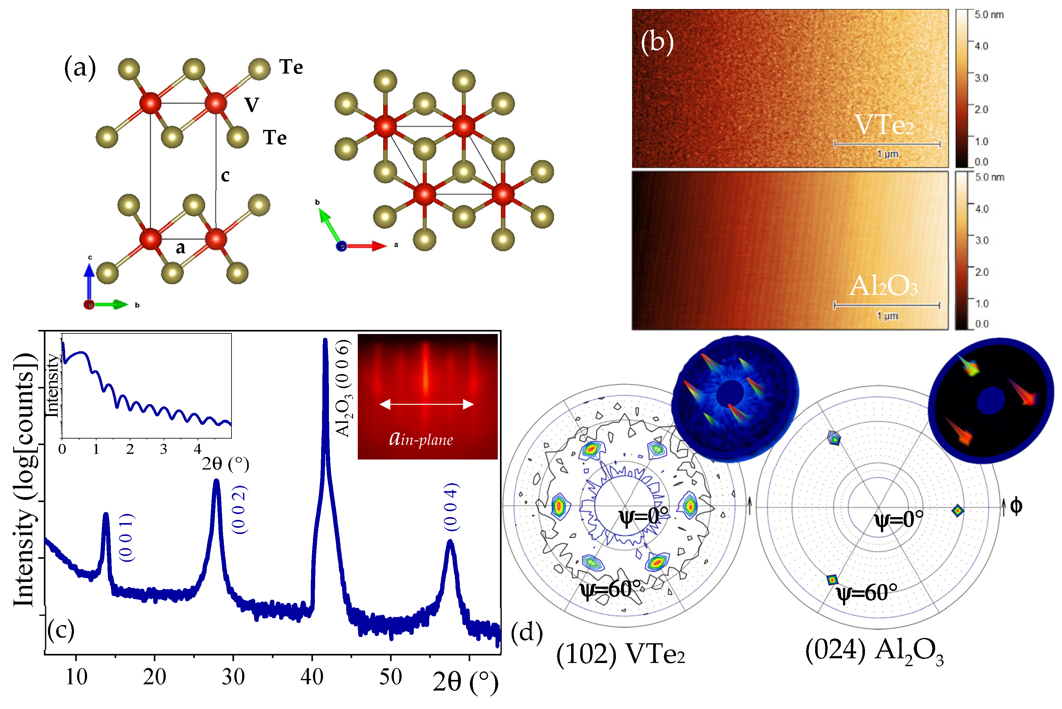
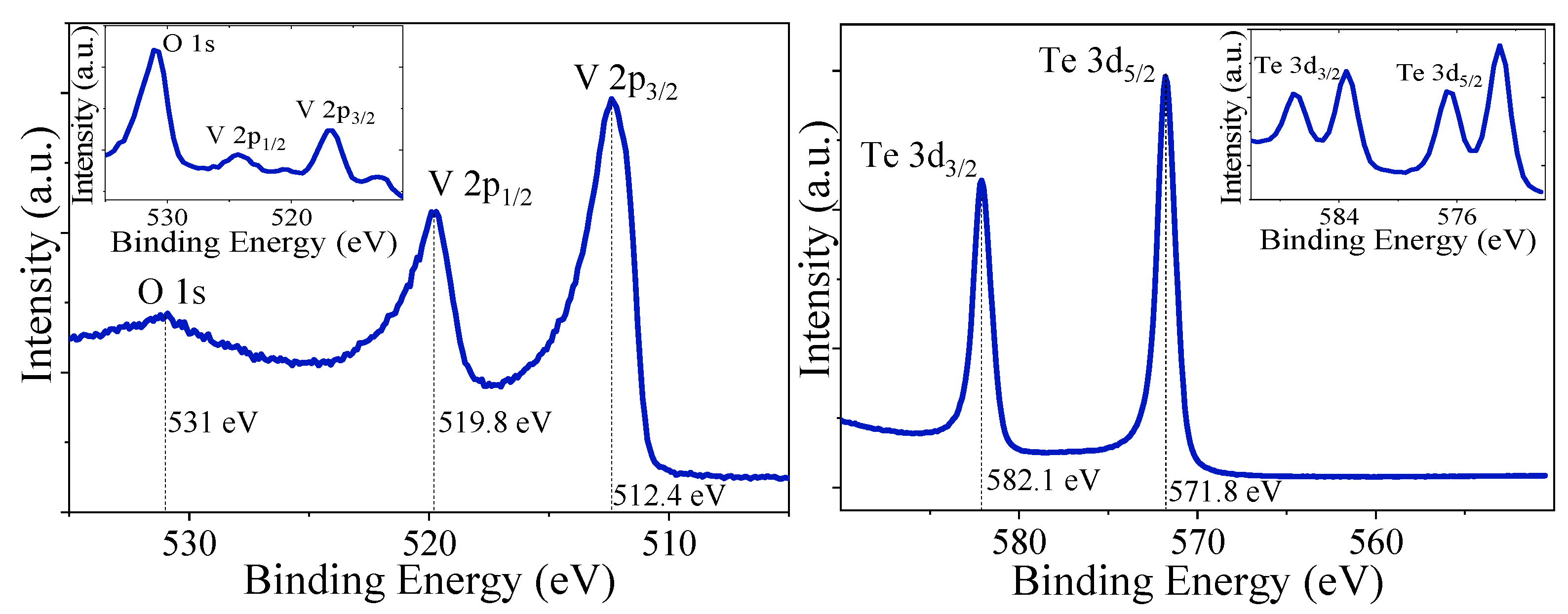
2. Materials and Methods

The VTe2 thin films were grown in an ultrahigh vacuum Octoplus 300 MBE System from Dr. Eberl MBE Komponenten in Te-rich conditions at 0.07 nm/min. V (99.99 %) and Te (99.9999%) were evaporated from a custom high-temperature effusion cell and standard Knudsen cell, respectively. Al2O3 (001) is an appropriate substrate for van der Waals epitaxy of TMD materials due to its atomically smooth surface without dangling bonds with a hexagonal lattice symmetry. Moreover, Al2O3 is an insulating substrate suitable for electrical measurements. Prior to the deposition, the substrate was thermally treated in air for 90 min at 1050 °C to obtain atomically flat terraces. Subsequently, the substrate was degassed in situ for 60 min at 500 °C in the presence of Te vapor. The result is an appropriate substrate for van der Waals epitaxy. Finally, the substrate temperature was decreased to 225 °C, at which the growth process was performed during the rotation of the sample. The base pressure during the growth was 1 × 10⁻¹⁰ mbar. The sample thickness ranges between a monolayer to a few layers. All the samples were in situ capped with 15 nm of Te (deposited at room temperature) to prevent possible oxidation.
X-ray diffraction (XRD) and X-ray reflectometry (XRR) measurements were collected using a Bruker D8 Dimension system in the Bragg–Brentano configuration. Texture analysis was performed by making pole diagrams using a Panalytical system positioning the detector at a fixed 2θ Bragg’s angle corresponding to a specific crystallographic plane. The diffracted beam intensity was mapped as the sample was rotated 360° around the azimuthal axis (φ) and tilted from 20° to 80° around the tilt axis (ψ). X-ray photoelectron spectroscopy (XPS) spectra were measured using an Omicron nanotechnology surface analysis system, equipped with a monochromatic aluminum source. The surface morphology was examined through atomic force microscopy (AFM) by means of a Bruker Dimension Icon system. AFM measurements were carried out in tapping mode to analyze the 3D surface topography. Low-temperature (4.5 K) transport measurements were carried out using an Oxford 4He cryostat equipped with a 7T superconducting magnet, connected to a lock-in amplifier measurement set up to send/measure the AC current/voltage. Hall bar devices (410 × 820 mm) were fabricated by optical lithography. For this, OiR 907-17 photoresist was spin-coated over the surface of the sample at 4000 rpm for 60 s and baked for 1 min at 100 °C. After UV exposure, the sample was developed in AZ-351 for 1 min. Argon ion milling was used to structure the film. A second step of lithography was made to define the Au contacts using RF sputter deposition.

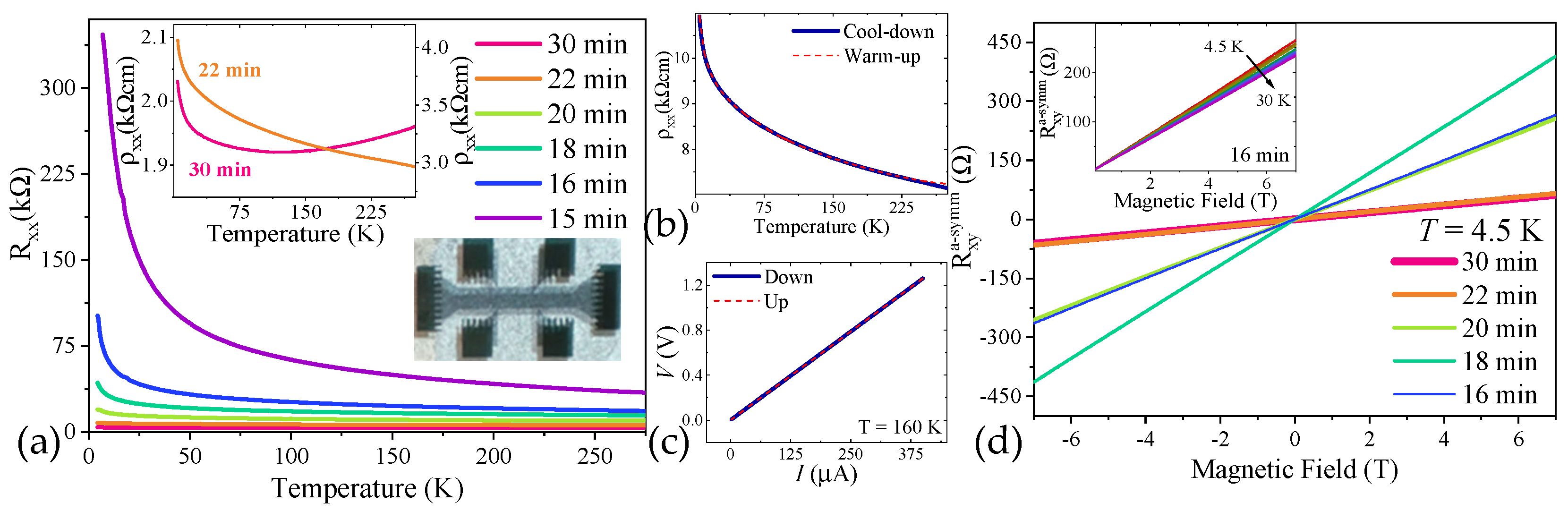
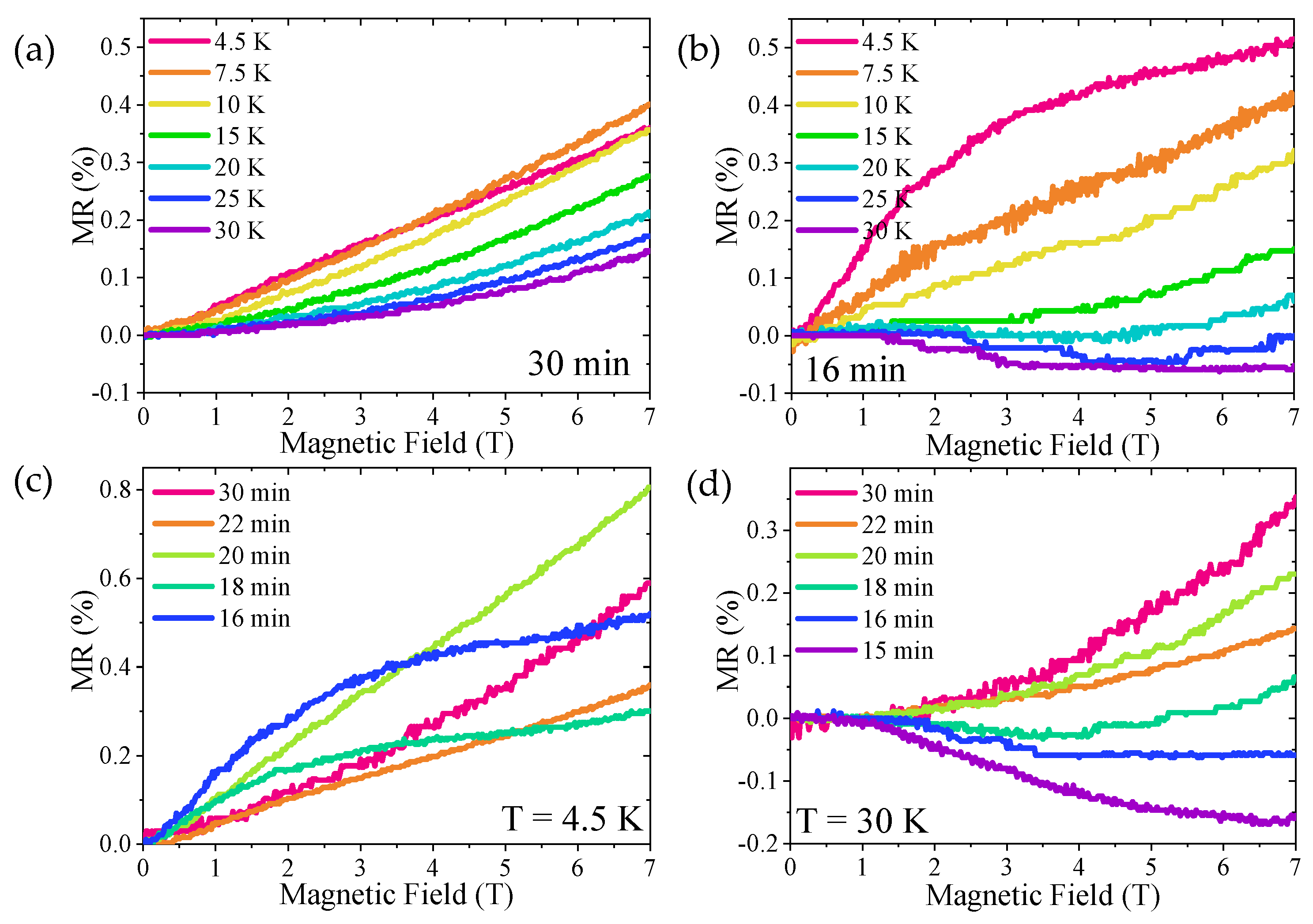
3. Results and Discussion

Bulk VTe2 presents a monoclinic distorted 1T’ phase below 207 °C [24,25] but recently it has been shown that an undistorted hexagonal 1T structure appears upon a reduction of the thickness [18]. Lattice distortions related to thickness, temperature, and electrical field have led to quantum phases such as charge density waves (CDWs) phases [26,27]. The 1T structure is composed of one layer of hexagonally arranged vanadium atoms sandwiched between two layers of tellurium atoms in an octahedral configuration, stacked together by weak van der Waals forces (Figure 1a). In a trigonal layered structure, 1T-VTe2 crystallizes in the space group P-3m1 with hexagonal lattice parameters of a = b = 3.64 Å and c = 6.51 Å [24,28,29].
The surface morphology was studied by AFM in Figure 1b. The 5 nm 1T-VTe2 sample has a smooth surface with a roughness of 170 pm. The terrace termination is similar to the Al2O3 substrate surface, which indicates an epitaxial growth. Figure 1c shows a typical XRD pattern corresponding to 15 nm 1T-VTe2 deposited on Al2O3 (001). The obtained material was identified as hexagonal VTe2 according to Powder Diffraction File 98-060-3582 and other reports [22,26]. The presence of only the (00l) family peaks indicate that the obtained films have the c-axis of the crystallites oriented perpendicular to the substrate surface. The thickness obtained by XRR was 15.7 nm (left inset in Figure 1c). Using Bragg’s law, the estimated c-axis lattice constant was calculated to be 6.58 Å, which is in good agreement with the expected value for 1T-VTe2. The in-plane lattice constant extracted from the streak spacing obtained by the reflection high-energy diffraction (RHEED) patterns was 3.7 Å, also consistent with 1T-VTe2 (right inset in Figure 1c). The obtained lattice parameter discards the presence of the 1T’ structure or phases related to the CDWs transitions.
The in-plane orientation and the epitaxial relation with the substrate were studied through texture analysis. Figure 1d shows the pole diagram taken at 2θ = 39.6° corresponding to the (102) crystalline plane of VTe2. The well-defined peaks around ψ = 46° correspond with the angle between the (001) and (102) crystalline planes of VTe2. The presence of the six distinct peaks is in agreement with the six-fold symmetry of the 1T-VTe2 hexagonal structure and is an indication of the in-plane orientation of the crystals. The pole diagram corresponding to the (024) crystalline plane of Al2O3 was also measured. The obtained peaks are at the same ϕ angle as the VTe2 peaks, which means that the VTe2 films are growing according to a textured epitaxial growth mode, i.e., both the c- and a-axis are oriented with respect to the substrate axes [30].
In situ high-resolution XPS spectra for V-2p and Te-3d of 5 nm 1T-VTe2 thin films are given in Figure 2. Both spectra are composed of one chemical state, without metallic or oxidized bonding. The binding energies of the distinct V-2p and Te-3d doublet peaks indicate that the VTe2 film consists of the 1T-VTe2 phase [24,25]. The stoichiometry of the grown film was calculated by fitting the XPS peaks, for which we performed a Shirley background subtraction from the data. As a result, we found a V:Te ratio of 1:2.09, consistent with VTe2. Ex situ measurements showed high levels of oxidation, which means that for an ex situ study of thin samples (<5 nm) a capping layer is required (see double peaks in the insets in Figure 2).
Low-temperature magnetoelectric transport measurements were performed on thin VTe2 films (less than 2 nm thick) using a Hall bar configuration (right inset in Figure 3a) in an out-of-plane magnetic field direction. Considering a non-linear growth rate during the initial stage of the growth and a capping with 10 nm of Te to avoid oxidation, an absolute estimate of the thickness was not made. Therefore, we quote the growth time when we compare different samples. In addition, considering previous reports on the use of Te as a capping layer in other material systems [31,32], where a slight change in the nominal value of the resistance while keeping the same magnetoelectric behavior was observed, we could safely neglect the effect of the Te capping layer on our measurements.
The temperature-dependent resistivity of samples with different thicknesses is shown in Figure 3a. For the thicker 1T-VTe2 sample (30 min), the resistivity shows a small decrease with decreasing temperature, suggesting a metallic behavior, typical of bulk VTe2 (left inset in Figure 3a) [21] with a slight increase of the resistance below 105 K. Upon decreasing the growth time (<30 min), we observed semiconducting behavior in the entire temperature range, i.e., an increase in resistivity while decreasing the temperature. The thinnest samples show the largest increase in resistivity reaching resistances in the order of MOhms at 7 K, leaving the film nearly insulating and no longer possible to be measured with our lock-in configuration. These results are in agreement with previous reports that attribute the strong thickness-dependent metal to insulator transition to two different patterns of CDW phases in VTe2 films [27,29]. However, no sudden step in resistance, characteristic of CDW phase transitions driven by temperature and/or electrical field (DC current), was observed during the cool-down and warm-up of the samples (Figure 3b,c).
No magnetic field hysteresis loop was observed, independently of the film thicknesses and temperature, which indicates that no intrinsic long-range ferromagnetic order occurs (Figure 3d). The absence of hysteresis loops was confirmed for in-plane oriented applied magnetic fields. Therefore, we can conclude that no anomalous Hall effect was observed in any of the VTe2 samples. These results are in line with the results from previous studies performed using ARPES [17] and X-ray magnetic circular dichroism measurements [18]. Extracting the Hall resistance, the sheet carrier concentration (n2D) and the carrier mobility (μ) were calculated. Upon decreasing the thickness, n2D decreased from 7.02 × 10¹³ to 1.89 × 1013 cm−2 while μ ranged from 43.8 to 1.9 cm2/Vs. For a temperature range of 4.5 to 30 K (inset in Figure 3d), the electrical conduction is dominated by p-type charge carriers, consistent with the hole-like bands determined by ARPES [33] and the Hall measurements in VTe2 single crystals [34].
Figure 4 reveals the magnetoresistance as a function of perpendicular magnetic field (MR = (ρxx(B)−ρxx(0))/ρxx(0) × 100%) for a thick (a) and thin (b) VTe2 sample at various temperatures and VTe2 samples of different thicknesses at 4.5 K (c) and 30 K (d). For thicker samples (Figure 4a), a positive and quadratic field dependence MR is observed independent of temperature, which is in agreement with the classical theory of ordinary MR. However, for thinner samples at low temperature (4.5 K), the MR is linear with a steep slope at low magnetic fields and a shallow slope above approximately 3 T (Figure 4b). Moreover, contrary to the thicker sample, the MR undergoes a gradual transition from positive to negative increasing the temperature. The influence of the VTe2 film thickness on the electronic properties of the material is clearer in Figure 4c,d. At 4.5 K, a positive MR is obtained for all the samples while at 30 K a transition from positive to negative MR appears by decreasing the film thickness. Negative MR has been reported in VTe2 nanoplates of approximately 87 nm deposited by CVD [21] or single crystals [34]. This behavior is attributed to the Kondo effect, which is related to the presence of localized magnetic moments even when there is no sign of intrinsic long-range ferromagnetism. This effect is characterized by negative MR at temperatures below the so-called Kondo temperature, and in our films, there is a transition from positive to negative MR with increasing temperature. Therefore, we must rule out this effect as the origin of the negative MR observed in our thin films.

4. Conclusions

High-quality 1T phase VTe2 thin films have been grown by MBE. Our experimental findings show no signs of intrinsic long-range ferromagnetic order and clearly demonstrate that our VTe2 films exhibit non-trivial temperature-dependent magneto-transport properties. The MR behavior of VTe2 films can be tuned by varying the thickness and temperature. This provides important insights to design sign-adjustable magneto-electronic devices. Further studies of the resistivity at low temperatures and under different magnetic fields and angle-dependent MR studies are still needed to understand the origin of the MR behavior of VTe2.

Author Contributions

Conceptualization, O.C. and A.B.; methodology, O.C., L.M. and D.H.W.; validation, O.C., L.M. and D.H.W.; investigation, O.C., L.M. and D.H.W.; writing—original draft preparation, O.C.; writing—review and editing, O.C., L.M., D.H.W. and A.B.; visualization, O.C., L.M. and D.H.W.; supervision, O.C. and A.B.; funding acquisition, A.B. All authors have read and agreed to the published version of the manuscript.

Funding

This research was funded by the Netherlands Organization for Scientific Research (NWO) through a VICI grant. The funders had no role in the design of the study; in the collection, analyses, or interpretation of data; in the writing of the manuscript; or in the decision to publish the results.

Data Availability Statement

Not applicable.

Acknowledgments

The authors thank F.J.G. Roesthuis for all technical support.

Conflicts of Interest

The authors declare no conflict of interest. The funders had no role in the design of the study; in the collection, analyses, or interpretation of data; in the writing of the manuscript; or in the decision to publish the results.

References

  1. Pop, E.; Sinha, S.; Goodson, K. Heat Generation and Transport in Nanometer-Scale Transistors. Proc. IEEE 2006, 94, 1587–1601. [Google Scholar] [CrossRef]
  2. Fuh, H.-R.; Chang, C.-R.; Wang, Y.-K.; Evans, R.; Chantrell, R.; Jeng, H.-T. Newtype single-layer magnetic semiconductor in transition-metal dichalcogenides VX2 (X = S, Se and Te). Sci. Rep. 2016, 6, 32625. [Google Scholar] [CrossRef] [PubMed]
  3. Montoya, E.; Heinrich, B.; Girt, E. Quantum well state induced oscillation of pure spin currents in Fe/Au/Pd (001) systems. Phys. Rev. Lett. 2014, 113, 136601. [Google Scholar] [CrossRef] [PubMed]
  4. Wolf, S.A.; Awschalom, D.D.; Buhrman, R.A.; Daughton, J.M.; von Molnár, V.S.; Roukes, M.L.; Chtchelkanova, A.Y.; Treger, D.M. Spintronics: A spin-based electronics vision for the future. Science 2001, 294, 1488–1495. [Google Scholar] [CrossRef]
  5. Mak, K.F.; Lee, C.; Hone, J.; Shan, J.; Heinz, T.F. Atomically thin MoS2: A new direct-gap semiconductor. Phys. Rev. Lett. 2010, 105, 136805. [Google Scholar] [CrossRef]
  6. Bonilla, M.; Kolekar, S.; Ma, Y.; Diaz, H.C.; Kalappattil, V.; Das, R.; Eggers, T.; Gutierrez, H.R.; Phan, M.-H.; Batzill, M. Strong room-temperature ferromagnetism in VSe2 monolayers on van der Waals substrates. Nat. Nanotechnol. 2018, 13, 289–293. [Google Scholar] [CrossRef]
  7. Shabbir, B.; Nadeem, M.; Dai, Z.; Fuhrer, M.S.; Xue, Q.-K.; Wang, X.; Bao, Q. Long range intrinsic ferromagnetism in two dimensional materials and dissipationless future technologies. Appl. Phys. Rev. 2018, 5, 041105. [Google Scholar] [CrossRef]
  8. Sagar, R.U.R.; Shabbir, B.; Hasnain, S.M.; Mahmood, N.; Zeb, M.H.; Shivananju, B.; Ahmed, T.; Qasim, I.; Malik, M.I.; Khan, Q.; et al. Large magnetotransport properties in mixed-dimensional van der Waals heterostructures of graphene foam. Carbon 2020, 159, 648–655. [Google Scholar] [CrossRef]
  9. Chen, P.; Pai, W.W.; Chan, Y.-H.; Sun, W.-L.; Xu, C.-Z.; Lin, D.-S.; Chou, M.-Y.; Fedorov, A.; Chiang, T.-C. Large quantum-spin-Hall gap in single-layer 1T′ WSe2. Nat. Commun. 2018, 9, 2003. [Google Scholar] [CrossRef]
  10. Xi, X.; Wang, Z.; Zhao, W.; Park, J.-H.; Law, K.T.; Berger, H.; Forró, L.; Shan, J.; Mak, K.F. Ising pairing in superconducting NbSe2 atomic layers. Nat. Phys. 2015, 12, 139–143. [Google Scholar] [CrossRef] [Green Version]
  11. Musle, V.; Kumar, A.; Choudhary, S. Temperature dependent spin transport investigations in single layer VTe2. J. Alloy. Compd. 2018, 770, 345–349. [Google Scholar] [CrossRef]
  12. Vatansever, E.; Sarikurt, S.; Evans, R.F.L. Hysteresis features of the transition-metal dichalcogenides VX2(X = S, Se, and Te). Mater. Res. Express 2018, 5, 046108. [Google Scholar] [CrossRef]
  13. Pan, H. Electronic and Magnetic Properties of Vanadium Dichalcogenides Monolayers Tuned by Hydrogenation. J. Phys. Chem. C 2014, 118, 13248–13253. [Google Scholar] [CrossRef]
  14. Begunovich, L.V.; Kuklin, A.V.; Visotin, M.A.; Kuzubov, A.A.; Tomilin, F.N.; Tarasov, A.S.; Mikhalev, Y.G.; Avramov, P.V. Triple VTe2/graphene/VTe2 heterostructures as perspective magnetic tunnel junctions. Appl. Surf. Sci. 2020, 510, 145315. [Google Scholar] [CrossRef]
  15. Li, J.; Zhao, B.; Chen, P.; Wu, R.; Li, B.; Xia, Q.; Guo, G.; Luo, J.; Zang, K.; Zhang, Z.; et al. Synthesis of Ultrathin Metallic MTe2 (M = V, Nb, Ta) Single-Crystalline Nanoplates. Adv. Mater. 2018, 30, e1801043. [Google Scholar] [CrossRef]
  16. Wong, P.K.; Zhang, W.; Zhou, J.; Bussolotti, F.; Yin, X.; Zhang, L.; N’Diaye, A.T.; Morton, S.A.; Chen, W.; Goh, J.; et al. Metallic 1T Phase, 3d1 Electronic Configuration and Charge Density Wave Order in Molecular Beam Epitaxy Grown Monolayer Vanadium Ditelluride. ACS Nano 2019, 13, 12. [Google Scholar] [CrossRef]
  17. Wang, Y.; Ren, J.; Li, J.; Wang, Y.; Peng, H.; Yu, P.; Duan, W.; Zhou, S. Evidence of charge density wave with anisotropic gap in a monolayer VTe2 film. Phys. Rev. B 2019, 100, 241404. [Google Scholar] [CrossRef]
  18. Coelho, P.M.; Lasek, K.; Nguyen Cong, K.; Li, J.; Niu, W.; Liu, W.; Oleynik, I.I.; Batzill, M. Monolayer Modification of VTe2 and Its Charge Density Wave. J. Phys. Chem. Lett. 2019, 10, 4987–4993. [Google Scholar] [CrossRef]
  19. Liu, Z.-L.; Wu, X.; Shao, Y.; Qi, J.; Cao, Y.; Huang, L.; Liu, C.; Wang, J.-O.; Zheng, Q.; Zhu, Z.-L.; et al. Epitaxially grown monolayer VSe 2: An air-stable magnetic two-dimensional material with low work function at edges. Sci. Bull. 2018, 63, 419–425. [Google Scholar] [CrossRef]
  20. Feng, J.; Biswas, D.; Rajan, A.; Watson, M.D.; Mazzola, F.; Clark, O.J.; Underwood, K.; Marković, I.; McLaren, M.; Hunter, A.; et al. Electronic Structure and Enhanced Charge-Density Wave Order of Monolayer VSe2. Nano Lett. 2018, 18, 4493–4499. [Google Scholar] [CrossRef] [PubMed]
  21. Liu, H.; Xue, Y.; Shi, J.-A.; Guzman, R.A.; Zhang, P.; Zhou, Z.; He, Y.; Bian, C.; Wu, L.; Ma, R.; et al. Observation of the Kondo Effect in Multilayer Single-Crystalline VTe2 Nanoplates. Nano Lett. 2019, 19, 8572–8580. [Google Scholar] [CrossRef]
  22. Shi, J.; Huan, Y.; Zhao, X.; Yang, P.; Hong, M.; Xie, C.; Pennycook, S.; Zhang, Y. Two-Dimensional Metallic Vanadium Ditelluride as a High-Performance Electrode Material. ACS Nano 2021, 15, 1858–1868. [Google Scholar] [CrossRef]
  23. Li, X.; Zhu, Z.; Yang, Q.; Cao, Z.; Wang, Y.; Meng, S.; Sun, J.; Gao, H. Monolayer puckered pentagonal VTe2: An emergent two-dimensional ferromagnetic semiconductor with multiferroic coupling. Nano Res. 2021, 15, 1486–1491. [Google Scholar] [CrossRef]
  24. Hossain, M.; Iqbal, M.A.; Wu, J.; Xie, L. Chemical vapor deposition and temperature-dependent Raman characterization of two-dimensional vanadium ditelluride. RSC Adv. 2021, 11, 2624–2629. [Google Scholar] [CrossRef]
  25. Lasek, K.; Coelho, P.M.; Zberecki, K.; Xin, Y.; Kolekar, S.K.; Li, J.; Batzill, M. Molecular Beam Epitaxy of Transition Metal (Ti-, V-, and Cr-) Tellurides: From Monolayer Ditellurides to Multilayer Self-Intercalation Compounds. ACS Nano 2020, 14, 8473–8484. [Google Scholar] [CrossRef]
  26. Won, D.; Kiem, D.H.; Cho, H.; Kim, D.; Kim, Y.; Jeong, M.Y.; Seo, C.; Kim, J.; Park, J.; Han, M.J.; et al. Polymorphic Spin, Charge, and Lattice Waves in Vanadium Ditelluride. Adv. Mater. 2020, 32, e1906578. [Google Scholar] [CrossRef]
  27. Dai, T.; Kang, S.; Ma, X.; Dang, S.; Li, H.; Ruan, Z.; Zhou, W.; Hu, P.; Li, S.; Wu, S. Multiple Transitions of Charge Density Wave Order in Epitaxial Few-Layered 1T′-VTe2 Films. J. Phys. Chem. C 2019, 123, 18711–18716. [Google Scholar] [CrossRef]
  28. Liu, M.; Wu, C.; Liu, Z.; Wang, Z.; Yao, D.-X.; Zhong, D. Multimorphism and gap opening of charge-density-wave phases in monolayer VTe2. Nano Res. 2020, 13, 1733–1738. [Google Scholar] [CrossRef]
  29. Ma, X.; Dai, T.; Dang, S.; Kang, S.; Chen, X.; Zhou, W.; Wang, G.; Li, H.; Hu, P.; He, Z.; et al. Charge Density Wave Phase Transitions in Large-Scale Few-Layer 1T-VTe2 Grown by Molecular Beam Epitaxy. ACS Appl. Mater. Interfaces 2019, 11, 10729–10735. [Google Scholar] [CrossRef]
  30. Fewster, P.F. X-ray Scattering from Semiconductors. X-ray Scatt. Semicond. 2003. [Google Scholar] [CrossRef]
  31. Ngabonziza, P.; Stehno, M.P.; Myoren, H.; Neumann, V.A.; Koster, G.; Brinkman, A. Gate-Tunable Transport Properties of In Situ Capped Bi2 Te3 Topological Insulator Thin Films. Adv. Electron. Mater. 2016, 2, 1600157. [Google Scholar] [CrossRef]
  32. Hoefer, K.; Becker, C.; Wirth, S.; Tjeng, L.H. Protective capping of topological surface states of intrinsically insulating Bi2Te3. AIP Adv. 2015, 5, 097139. [Google Scholar] [CrossRef]
  33. Sugawara, K.; Nakata, Y.; Fujii, K.; Nakayama, K.; Souma, S.; Takahashi, T.; Sato, T. Monolayer VTe2: Incommensurate Fermi surface nesting and suppression of charge density waves. Phys. Rev. B 2019, 99, 241404. [Google Scholar] [CrossRef]
  34. Ding, X.; Xing, J.; Li, G.; Balicas, L.; Gofryk, K.; Wen, H.-H. Crossover from Kondo to Fermi-liquid behavior induced by high magnetic field in 1T−VTe2 single crystals. Phys. Rev. B 2021, 103, 125115. [Google Scholar] [CrossRef]
Figure 1. (a) Schematic side- and top-view of the crystal structure of 1T-VTe2. (b) AFM image of 5 nm 1T-VTe2 thin film (top) and Al2O3 (001) substrates (bottom). Both show a smooth terrace termination. (c) XRD pattern of a VTe2 thin film deposited on an Al2O3 (001) substrates. Miller indices of the corresponding planes are indicated. Insets: XRR reveals oscillations that correspond to a thickness of 15.7 nm and RHEED with streaks corresponding to a = 3.66 Å. (d) Pole diagram measured at 2θ = 39.6° and 2θ = 52.6° corresponding to the (102) and (024) crystalline plane of VTe2 and Al2O3, respectively.
Solids 03 00033 g001
Figure 2. In situ high-resolution XPS spectra of a 5 nm VTe2 thin films deposited on Al2O3 substrates showing solely V-2p and Te-3d doublet peaks, respectively, indicating homogeneous phases of 1T-VTe2. Insets: ex situ measurements showing the presence of oxidized states.
Solids 03 00033 g002
Figure 3. (a) Temperature-dependent resistivity of samples with different thicknesses. Left inset: behavior of the samples grown during 30 and 22 min. Right inset: optical image of a typical Hall bar used for magneto-electric transport measurements with a length and width of 820 μm and 410 μm, respectively. (b) Temperature-dependent resistivity during the cool-down and warm-up. (c) An exemplary I-V measurement taken at 160 K. (d) Hall resistance as function of perpendicular applied magnetic field. Inset: temperature-dependent Hall measurements corresponding to the VTe2 sample grown during 16 min.
Solids 03 00033 g003
Figure 4. Magnetoresistance at different temperatures of a thick (a) and a thin (b) VTe2 film. A transition from positive to negative MR is observed for the thin sample above 15 K. Magnetoresistance for different VTe2 film thicknesses at 4.5 K (c) and 30 K (d).
Solids 03 00033 g004
Publisher’s Note: MDPI stays neutral with regard to jurisdictional claims in published maps and institutional affiliations.

