Proceeding Paper

Impact of Hole Transport Layers in Inorganic Lead-Free B-γ-CsSnI3 Perovskite Solar Cells: A Numerical Analysis †

1
Department of Electrical, Electronic and Communication Engineering, Pabna University of Science and Technology, Pabna 6600, Bangladesh
2
Laboratoire de Rayonnement et Plasmas et Physique des Surfaces (LRPPS), Université Kasdi Merbah, Ouargla 30000, Algeria
*
Authors to whom correspondence should be addressed.
Presented at the 1st International Electronic Conference on Processes: Processes System Innovation, 17–31 May 2022; Available online: https://sciforum.net/event/ECP2022.
Eng. Proc. 2022, 19(1), 41; https://doi.org/10.3390/ECP2022-12611
Published: 17 May 2022

Abstract

:
Tin-based halide perovskite compounds have attracted enormous interest as effective replacements for the conventional lead halide perovskite solar cells (PCSs). However, achieving high efficiency for tin-based perovskite solar cells is still challenging. Herein, we introduced copper sulfide (CuS) as a hole transport material (HTM) in lead free tin-based B-γ-CsSnI3 PSCs to enhance the photovoltaic (PV) performances. The lead free tin-based CsSnI3 perovskite solar cell structure consisting of CuS/CsSnI3/TiO2/ITO was modeled and the output characteristics were investigated by using the one dimensional solar cell capacitance simulator (SCAPS-1D). The CuS hole transport layer (HTL) with proper band arrangement may notably minimize the recombination of the charge carrier at the back side of the perovskite absorber. Density functional theory (DFT)-extracted physical parameters including the band gap and absorption spectrum of CuS were used in the SCAPS-1D program to analyze the characteristics of the proposed PV device. The PV performance parameters of the proposed device were numerically evaluated by varying the absorber thickness and doping concentration. In this work, the variation of the functional temperature on the cell outputs was also studied. Furthermore, different HTMs were employed to investigate the PV characteristics of the proposed CsSnI3 PSC. The power conversion efficiency (PCE) of ~29% was achieved with open circuit voltage (Voc) of 0.99 V, a fill factor of ~87%, and short circuit current density (Jsc) of 33.5 mA/cm2 for the optimized device. This work addressed guidelines and introduced a convenient approach to design and fabricate highly efficient, inexpensive, and stable lead free tin-based perovskite solar cells.

1. Introduction

PSCs have attracted great attention as promising PV technologies due to their admirable properties associated with excellent PCE and low fabrication cost. This new class of PV technology has recently received enormous interest owing to the emerging conversion efficiency of ~25% [1,2]. However, the rapid growth and commercialization of PSCs are impeded because of toxicity present in most commonly developed lead-based perovskite solar cells [3]. In this context, various attempts have been made in pursuit of suitable alternative for the lead-based perovskites [4,5,6]. Among different perovskite materials, the inorganic cesium tin triiodide (CsSnI3) may be considered as one of the potential candidates [7]. CsSnI3 exhibits suitable optoelectronic properties including an ideal energy gap of ~1.3 eV, absorption coefficient (104 cm−1), high charge-carrier mobilities (above 500 cm2 V−1 s−1) and low exciton binding energy (~18 meV) [7,8]. In the previous work, an efficiency of 0.9% was reported with the architecture of indium tin oxide/CsSnI3/Au/Ti in 2012 [9]. An earlier work evaluated a maximum power conversion efficiency (PCE) of 5.03% for CsSnI3 PVQD-based solar cells [10]. Recently, an enhanced efficiency of 6.08% was measured experimentally by using mixed electron transport layer with a CsSnI3 absorber [11]. Another recent work shows the highest experimental conversion efficiency of 7.50% for the configuration of a CsSnI3 absorber with poly (3-hexylthiophene) as HTL [12]. Very recently, a numerical work on the TiO2/CsSnI3/Spiro-OMeTAD PSC evaluated a power conversion efficiency of 20.2% with Voc of 0.97 V [13]. However, these efficiencies are still lower than the other available lead-based PSCs. For a PSC to operate efficiently, the HTL material is a pivotal factor. Insertion of HTL can speed up the hole extraction along with the minimization of carrier recombination by blocking the electron flow [14]. In this work, for the first time, we introduced copper sulfide (CuS) as a hole transport material with the CsSnI3 absorber with TiO2 as a electron transport layer (ETL). CuS is a p-type semiconducting material which was previously utilized as HTL with other inorganic solar cells [15]. The suitable semiconducting properties of CuS attained from DFT-extraction in the present work [16,17,18] provide proper band alignment with CsSnI3 to reduce the carrier recombination and enhance the PV performance of the cell.
This work represents the simulation and performance analysis of the PSC with the novel architecture of CuS/CsSnI3/TiO2/ITO by utilizing the SCAPS-1D program. To achieve the optimized performance, the output parameters were evaluated by varying the thickness, doping concentration, and bulk defect density of the absorber.

2. Methods and Materials

This present work performed first principle DFT utilizing Cambridge Serial Total Energy Package (CASTEP) open-source package [19] on CuS HTL to evaluate the optical and electrical properties and designed a novel heterojunction lead-free CsSnI3 PSC with an arrangement of CuS/CsSnI3/TiO2/ITO. The designed PSC was investigated numerically using the SCAPS-1D with Poisson’s and continuity equation to evaluate one and two-dimension semiconductor cells [20]. In the present study, CuS and TiO2 were utilized as an HTL at the back of the absorber and ETL, respectively. Indium tin oxide (ITO), as a transparent conducing oxide (TCO), was used in this numerical investigation. Aluminum (Al) with a work function of 4.06 eV [21] and Nickel (Ni) with a work function of 5.15 eV [21] were used as metallic electrodes at the front contact and back contact, respectively. Table 1 illustrates the electrical and optical parameters used in this numerical investigation to evaluate the output characteristics of the proposed device. The parameters of all the layers agreed well with some previous experimental and theoretical works [22,23,24,25,26,27,28,29,30].

3. Result and Discussion

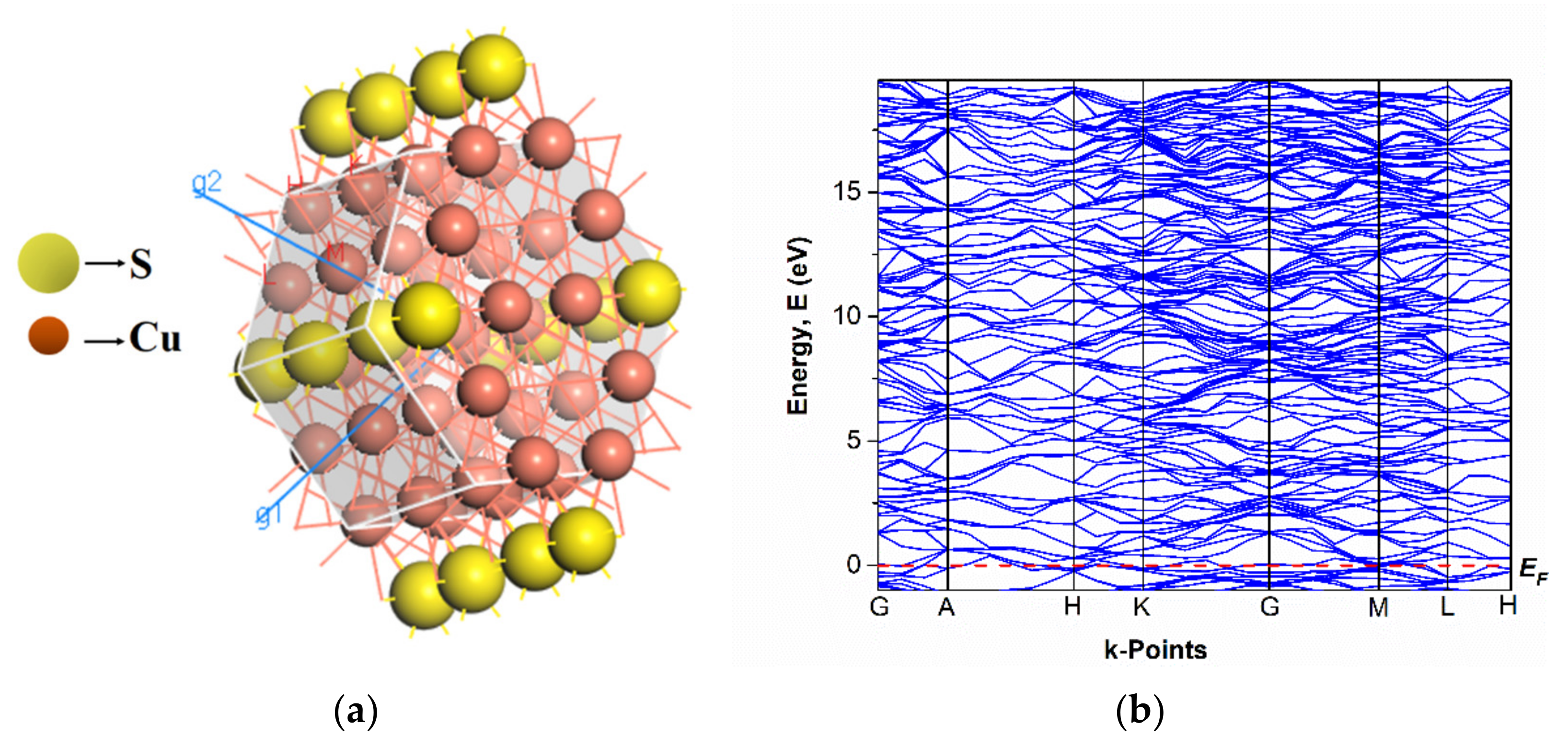
3.1. Structural Properties and Band Structure of CuS

In this study, the CASTEP toolkit package [19] was used for geometry optimization, elastic constants, band structure, density of states, and optical properties computation. The cut-off kinetic-energy of the plane wave was 400 eV with grid parameters (a × b × c) of 10 × 10 × 2 with an actual spacing 0.014296 × 0.014296 × 0.014327 1/Å. The lowest deviation of 27.1% was calculated using the initial cell volume and final optimized cell volume at a cutoff energy of 400 eV. The generalized gradient approximation (GGA) for the exchange correlation energy was taken, instead of local density approximation (LDA), due to its excellent band structure calculation. The lattice parameters of CuS are a = b = 3.797 Å, c = 16.441 Å, α = β = 90°, γ = 120° [31]. The geometry optimized crystal structure of the unit cell is depicted in Figure 1a. Figure 1b shows the band structure for the optimized CuS structure which is in good agreement with the density of state. The band structure calculation also shows the band-gap of ~1.6 eV. The band-gap analysis of CuS via DFT calculations with an hexagonal structure is almost in concurrence with the band-gap of the hole transport layer (CuS ~ 1.5 eV).

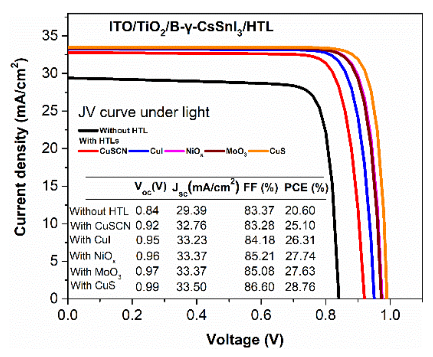
3.2. Impact of HTLs on Device Performances

To perceive the characteristics of the designed CsSnI3 PSC, numerous HTLs were investigated in this study and the resulting current density–voltage (J-V) characteristics are revealed in Figure 2. This work introduced several HTLs including CuSCN, CuI, CuS, NiOx, and MoO3 at the back of the CsSnI3 perovskite absorber to improve the proposed device performances by minimizing the losses of charge carrier recombination at the back of the absorber. It is noticed from Figure 2 that lead-free tin-based CsSnI3 PSC performances such as open-circuit voltage (Voc), short circuit current density (Jsc), power conversion efficiency (PCE), and fill factor (FF) improved after inserting the defined HTLs. By inserting HTLs, a strong built-in electric field is created at the back of the absorber, thus resulting in the improvement of Voc of the proposed device. Consequently, Jsc was also enhanced as the conduction of the charge carrier from absorber to back metal contact and the collection of charge carrier by the electrode eased. Additionally, introducing HTLs at the back of the absorber may reduce the recombination losses at the back interface and increase the performances of the device. Furthermore, it is important to select the proper HTL among the defined HTLs. A lower negative valance band offset (VBO) is needed to accumulate the holes from the absorber and create the proper band alignment, thus increasing the cell efficiency. Among the different HTLs, CuS has lower VBO than others and gives higher cell outputs which are also illustrated in Figure 2 (inset). Therefore, CuS as HTL was introduced in lead-free CsSnI3 PSC.

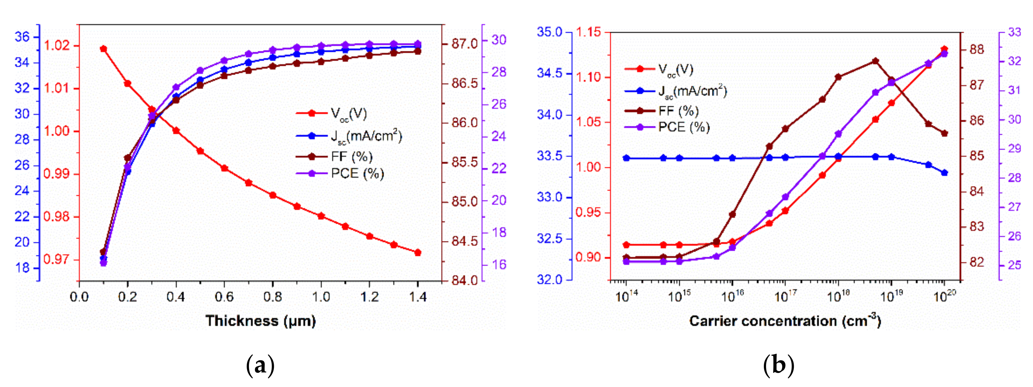
3.3. Effect of Absorber Thickness on Cell Performances

The photon energy was absorbed by the absorber layer. In order to realize the device characteristics, the thickness of the CsSnI3 perovskite absorber layer was shifted from 0.1 µm to 1.4 µm, as presented in Figure 3a. Thicknesses of 0.1 µm, 0.05 µm, and 0.05 µm for CuS HTL, TiO2 ETL, and ITO, respectively, were fixed during the analysis of absorber layer thickness. It was revealed that Voc decreased with an increased absorber layer thickness till 1.2 µm and then it almost became saturated. The degradation of Voc with absorber thickness can be described as the increment of series resistance and recombination rate. On the contrary, Jsc linearly increased up to the absorber thickness of 0.4 µm as the improved generated charge carriers and a comparatively small increment of Jsc were observed beyond the thickness of 0.5 µm. The absorption of light is significantly lower when the thickness of the absorber layer is lower; therefore, a thicker absorber is needed to absorb sufficient light for enhancing the current density and efficiency. The variation of the fill factor (FF) did not changed notably throughout the entire thickness of the absorber. In addition, the PCE improved up to the absorber thickness of 0.6 µm. Beyond 0.6-µm-thick, a less significant enhancement of the PCE was observed. Therefore, absorber thickness was optimized to be 0.6 µm. At the thickness of 0.6 µm, PCE was recorded to be 28.76%, including Voc of 0.99 V, Jsc of 33.5 mA/cm2, and an FF of 86.6% in the present study.

3.4. Effect of Carrier Concentration on Cell Performances

To perceive the output characteristics of the proposed device in accordance with the carrier concentration of the absorber, the range from 1014 cm−3 to 1020 cm−3 of carrier concentration of the absorber was examined. Figure 3b represents the variation of carrier concentration of the absorber. During the investigation of the doping density of the absorber, a doping density of 1019 cm−3, 1018 cm−3, and 1021 cm−3 for CuS HTL, TiO2 ETL, and ITO, respectively, were fixed. It is noticed from Figure 3b that the device output parameters such as Voc, FF, and PCE increased after boosting the doping density of the absorber. An improvement in the carrier concentration in the absorber layer may create enough charge carriers, thereby enhancing the PV performances of the perovskite solar device. The value of PCE > 28.76% and Voc > 0.99 V were measured when the doping density was larger than 5 × 1017 cm−3. Conversely, Jsc declined after boosting the absorber carrier concentration alongside the increment of augur recombination and resistivity of the absorber. At a doping density of 5 × 1017 cm−3, Jsc of 33.5 mA/cm2 was estimated. This work optimized the doping density of 5 × 1017 cm−3 considering the overall performances and this optimized value is consistent with the previous experimental works [27].

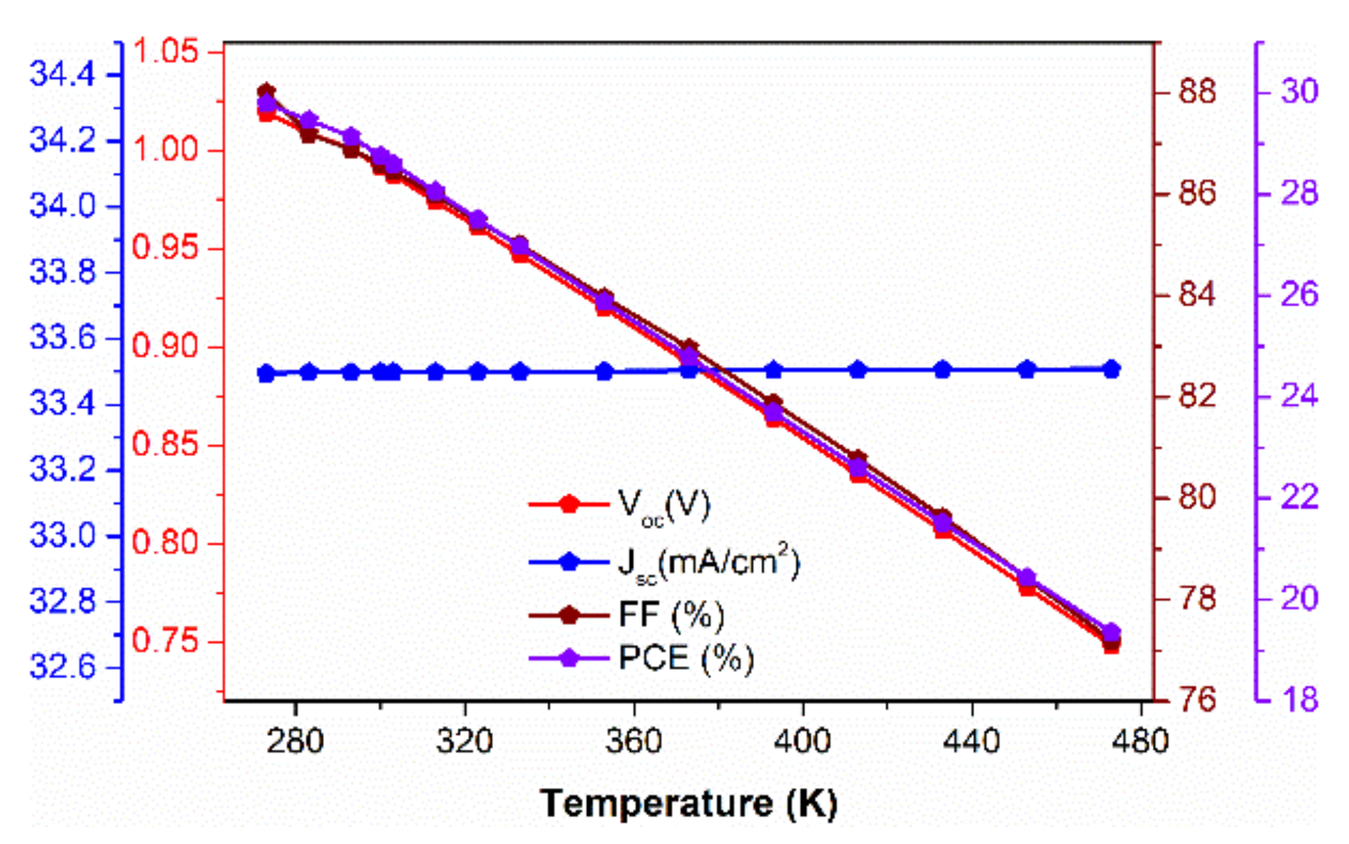
3.5. Effect of Temperature on Cell Performances

The characteristics and output parameters of solar cells are immensely dependent on temperature. The reduction in the energy bandgap of the material allows for the spare absorption of the photons of small energy which leads to an increase in the short-circuit current. On the other hand, reduction in the bandgap results in diminishing the open-circuit voltage [32,33]. In the interest of realizing the stability of PSCs, the influence of temperature on device performances was shifted from 283 K to 483 K as depicted in Figure 4. As is noticeable from the figure, the device output parameters including Voc, PCE, and FF declined with an increased conducting temperature. Voc of 1.02 V, PCE of 29.79%, and FF of 88.01% were determined at temperature of 273 K and these values reduced to 0.75 V, 77.2%, and 19.36% for Voc, PCE, and FF, respectively, at a temperature of 473 K. The value of Jsc was rarely increased with temperature at almost a constant owing to the reverse-saturation current density ameliorates with temperature [33].

4. Conclusions

This work designed lead-free tin- based B-γ-CsSnI3 PSC with the arrangement of CuS/CsSnI3/TiO2/ITO where the CuS was utilized as HTL, and TiO2 as ETL. Initially, some optical and electrical properties were analyzed for CuS HTL using the first principle density functional theory. After that, the characteristics of the proposed device structure were assessed numerically by using the SCAPS-1D. The PV performances were evaluated by varying the thickness and carrier concentration of the absorber layer. Herein, numerous HTLs were realized to adopt the worthy HTL for B-γ-CsSnI3 PSC. The best power conversion efficiency (PCE) of 28.76% containing Voc of 0.99 V, Jsc of 33.5 mA/cm2, and FF of 86.6% was attained with the optimized thicknesses of 0.1 µm, 0.6 µm, 0.05 µm, and 0.05 µm for the CuS HTL, absorber, TiO2 ETL, and ITO, respectively. After providing the overall examination on B-γ-CsSnI3 PSCs, this work recommend that CuS be utilized as a prominent HTL at the back of the absorber to design and fabricate earth-abundant and cost-effective B-γ-CsSnI3 PSC.

Author Contributions

Conceptualization, A.H.; methodology, A.H.; software, A.H.; validation, A.H.; formal analysis, A.H., M.B., S.R. and S.R.A.A.; investigation, A.H.; resources, A.H., S.R. and S.R.A.A.; data curation, A.H.; writing—original draft preparation, A.H. and S.R.; writing—review and editing, M.B. and S.R.A.A.; visualization, A.H., M.B., S.R. and S.R.A.A.; supervision, S.R.A.A. All authors have read and agreed to the published version of the manuscript.

Funding

This research received no external funding.

Institutional Review Board Statement

Not applicable.

Informed Consent Statement

Not applicable.

Data Availability Statement

The data that support the findings of this study are available on request from the corresponding author.

Acknowledgments

The authors also wish to thank Marc Burgelman and his companions, University of Gent, Belgium for providing the SCAPS simulation package.

Conflicts of Interest

The authors declare no conflict of interest.

References

  1. Kim, J.Y.; Lee, J.-W.; Jung, H.S.; Shin, H.; Park, N.-G. High-Efficiency Perovskite Solar Cells. Chem. Rev. 2020, 15, 7867–7918. [Google Scholar] [CrossRef] [PubMed]
  2. Kim, G.-H.; Kim, D.S. Development of perovskite solar cells with >25% conversion efficiency. Joule 2021, 5, 1033–1035. [Google Scholar] [CrossRef]
  3. Su, P.; Liu, Y.; Zhang, J.; Chen, C.; Yang, B.; Zhang, C.; Zhao, X. Pb-Based Perovskite Solar Cells and the Underlying Pollution behind Clean Energy: Dynamic Leaching of Toxic Substances from Discarded Perovskite Solar Cells. J. Phys. Chem. Lett. 2020, 11, 2812–2817. [Google Scholar] [CrossRef] [PubMed]
  4. Schileo, G.; Grancini, G. Lead or no lead? Availability, toxicity, sustainability and environmental impact of lead-free perovskite solar cells. J. Mater. Chem. C 2020, 9, 67–76. [Google Scholar] [CrossRef]
  5. Kanno, S.; Imamura, Y.; Hada, M. Alternative materials for perovskite solar cells from materials informatics. Phys. Rev. Mater. 2019, 3, 075403. [Google Scholar] [CrossRef]
  6. Giustino, F.; Snaith, H.J. Toward Lead-Free Perovskite Solar Cells. ACS Energy Lett. 2016, 1, 1233–1240. [Google Scholar] [CrossRef] [Green Version]
  7. Wang, N.; Zhou, Y.; Ju, M.-G.; Garces, H.F.; Ding, T.; Pang, S.; Zeng, X.C.; Padture, N.P.; Sun, X.W. Heterojunction-Depleted Lead-Free Perovskite Solar Cells with Coarse-Grained B-γ-CsSnI3 Thin Films. Adv. Energy Mater. 2016, 6, 1601130. [Google Scholar] [CrossRef]
  8. Chung, I.; Song, J.-H.; Im, J.; Androulakis, J.; Malliakas, C.D.; Li, H.; Freeman, A.J.; Kenney, J.T.; Kanatzidis, M.G. CsSnI3: Semiconductor or Metal? High Electrical Conductivity and Strong Near-Infrared Photoluminescence from a Single Material. High Hole Mobility and Phase-Transitions. J. Am. Chem. Soc. 2012, 134, 8579–8587. [Google Scholar] [CrossRef]
  9. Chen, Z.; Wang, J.J.; Ren, Y.; Yu, C.; Shum, K. Schottky solar cells based on CsSnI3 thin-films. Appl. Phys. Lett. 2012, 101, 093901. [Google Scholar] [CrossRef]
  10. Wang, Y.; Tu, J.; Li, T.; Tao, C.; Deng, X.; Li, Z. Convenient Preparation of CsSnI3 Quantum Dots, Excellent Stability, and the Highest Performance of Lead-Free Inorganic Perovskite Solar Cells So Far. J. Mater. Chem. A 2019, 7, 7683–7690. [Google Scholar] [CrossRef]
  11. Ma, S.; Gu, X.; Kyaw, A.K.; Wang, D.H.; Priya, S.; Ye, T. Fully Inorganic CsSnI3-Based Solar Cells with >6% Efficiency and Enhanced Stability Enabled by Mixed Electron Transport Layer. ACS Appl. Mater. Interfaces 2021, 13, 1345–1352. [Google Scholar] [CrossRef]
  12. Ye, T.; Wang, K.; Hou, Y.; Yang, D.; Smith, N.; Magill, B.; Yoon, J.; Mudiyanselage, R.R.H.H.; Khodaparast, G.A.; Wang, K.; et al. Ambient-Air-Stable Lead-Free CsSnI3 Solar Cells with Greater than 7.5% Efficiency. J. Am. Chem. Soc. 2021, 143, 4319–4328. [Google Scholar] [CrossRef]
  13. Lin, S.; Zhang, B.; Lü, T.-Y.; Zheng, J.-C.; Pan, H.; Chen, H.; Lin, C.; Li, X.; Zhou, J. Inorganic Lead-Free B-γ-CsSnI3 Perovskite Solar Cells Using Diverse Electron-Transporting Materials: A Simulation Study. ACS Omega 2021, 6, 26689–26698. [Google Scholar] [CrossRef]
  14. Głowienka, D.; Zhang, D.; Di Giacomo, F.; Najafi, M.; Veenstra, S.; Szmytkowski, J.; Galagan, Y. Role of Surface Recombination in Perovskite Solar Cells at the Interface of HTL/CH3NH3PbI3. Nano Energy 2019, 67, 104186. [Google Scholar] [CrossRef]
  15. Lei, H.; Fang, G.; Cheng, F.; Ke, W.; Qin, P.; Song, Z.; Zheng, Q.; Fan, X.; Huang, H.; Zhao, X. Enhanced efficiency in organic solar cells via in situ fabricated p-type copper sulfide as the hole transporting layer. Sol. Energy Mater Sol. Cells 2014, 128, 77–84. [Google Scholar] [CrossRef]
  16. Sheardy, A.T.; Arvapalli, D.M.; Wei, J. Novel microwave synthesis of near-metallic copper sulfide nanodiscs with size control: Experimental and DFT studies of charge carrier density. Nanoscale Adv. 2020, 2, 1054–1058. [Google Scholar] [CrossRef] [Green Version]
  17. Santos Cruz, J.; Mayén Hernández, S.A.; Paraguay Delgado, F.; Zelaya Angel, O.; Castanedo Pérez, R.; Torres Delgado, G. Optical and Electrical Properties of Thin Films of CuS Nanodisks Ensembles Annealed in a Vacuum and Their Photocatalytic Activity. Int. J. Photoenergy 2013, 2013, 1–9. [Google Scholar] [CrossRef] [Green Version]
  18. Yang, Y.-P.; Zhang, Z.-W.; Shi, Y.-L.; Feng, S.; Wang, W.-Z. Far-infrared conductivity of CuS nanoparticles measured by terahertz time-domain spectroscopy. Chin. Phys. B 2010, 19, 043302. [Google Scholar]
  19. Clark, S.J.; Segall, M.D.; Pickard, C.J.; Hasnip, P.J.; Probert, M.J.; Refson, K.; Payne, M.C. First principles methods using CASTEP. Z. Krist. 2005, 220, 567–570. [Google Scholar] [CrossRef] [Green Version]
  20. Burgelman, M.; Decock, K.; Niemegeers, A.; Verschraegen, J.; Degrave, S. SCAPS Manual (Version: 3.3.07). Department of Electronics and Information Systems, University of Gent, Belgium. Available online: http://scaps.elis.ugent.be (accessed on 10 March 2022).
  21. Michaelson, H.B. The work function of the elements and its periodicity. J. Appl. Phys. 1977, 48, 4729–4733. [Google Scholar] [CrossRef] [Green Version]
  22. Pitchaiya, S.; Natarajan, M.; Santhanam, A.; Asokan, V.; Yuvapragasam, A.; Madurai Ramakrishnan, V.; EPalanisamy, S.; Sundaram, S.; Velauthapillai, D. A Review on the Classifications of Organic/Inorganic/Carbonaceous Hole Transporting Materials for Perovskite Solar Cell Application. Arab. J. Chem. 2020, 13, 2526–2557. [Google Scholar] [CrossRef]
  23. Kumar, R.R.; Pandey, S.K. Performance evaluation and material parameter perspective of eco-friendly highly efficient CsSnGeI3 perovskite solar cell. Superlattices Microstruct. 2019, 135, 106273. [Google Scholar]
  24. Li, W.; Li, W.; Feng, Y.; Yang, C. Numerical analysis of the back interface for high efficiency wide band gap chalcopyrite solar cells. Sol. Energy 2019, 180, 207–215. [Google Scholar] [CrossRef]
  25. PVEducation. Available online: https://www.pveducation.org/pvcdrom/materials/cus (accessed on 3 May 2022).
  26. Chung, I.; Lee, B.; He, J.; Chang, R.P.H.; Kanatzidis, M.G. All-solid-state dye-sensitized solar cells with high efficiency. Nature 2012, 485, 486–489. [Google Scholar] [CrossRef]
  27. Wu, B.; Zhou, Y.; Xing, G.; Xu, Q.; Garces, H.F.; Solanki, A.; Goh, T.W.; Padture, N.P.; Sum, T.C. Long Minority-Carrier Diffusion Length and Low Surface-Recombination Velocity in Inorganic Lead-Free CsSnI3 Perovskite Crystal for Solar Cells. Adv. Funct. Mater. 2017, 27, 1604818. [Google Scholar] [CrossRef]
  28. Jung, H.S.; Park, N.G. Perovskite solar cells: From materials to devices. Small 2015, 11, 10–25. [Google Scholar] [CrossRef]
  29. Van de Krol, R.; Goossens, A.; Schoonman, J. Mott-Schottky analysis of nanometer-scale thin-film anatase TiO2. J. Electrochem. Soc. 1997, 144, 1723–1727. [Google Scholar] [CrossRef]
  30. Rahman, M.A. Enhancing the photovoltaic performance of Cd-free Cu2ZnSnS4 heterojunction solar cells using SnS HTL and TiO2 ETL. Sol. Energy 2021, 215, 64–76. [Google Scholar] [CrossRef]
  31. Materials Project. Available online: https://materialsproject.org/materials/mp-504/ (accessed on 3 May 2022).
  32. Varshni, Y.P. Temperature dependence of the energy gap in semiconductors. Physica 1967, 34, 149–154. [Google Scholar] [CrossRef]
  33. Singh, P.; Ravindra, N.M. Temperature dependence of solar cell performance-an analysis. Sol. Energy Mater. Sol. Cells 2012, 101, 36–45. [Google Scholar] [CrossRef]
Figure 1. (a) Crystal structure; (b) band structure of CuS.
Engproc 19 00041 g001
Figure 2. J-V characteristics and solar outputs with different HTLs.
Engproc 19 00041 g002
Figure 3. Characteristics of CsSnI3 perovskite solar cell with (a) absorber layer thickness; (b) carrier concentration.
Engproc 19 00041 g003
Figure 4. Influence of temperature on the designed perovskite solar cell.
Engproc 19 00041 g004
Table 1. Parameters used in this study to investigate the device numerically.
ParametersCuSCNCuINiOxMoO3CuSCsSnI3TiO2ITO
Bandgap, Eg (eV)3.63.13.831.551.33.23.5
Electron affinity, χ (eV)1.72.11.462.53.893.84.14.6
Electron/hole mobility (cm2 V−1 s−1)100/25100/43.912/2.825/10012/950/4000.00610/10
Thickness (µm)0.10.10.10.10.10.60.050.05
Carrier concentration (cm−3)1 × 10181 × 10181 × 10181 × 10184.7 × 10185 × 10171 × 10181 × 1021
Reference[22][22][23][24][25][8,26,27][28,29][30]
Publisher’s Note: MDPI stays neutral with regard to jurisdictional claims in published maps and institutional affiliations.

