Review

Review of Si-Based Thin Films and Materials for Thermoelectric Energy Harvesting and Their Integration into Electronic Devices for Energy Management Systems

by
Carlos Roberto Ascencio-Hurtado
1,2,
Roberto C. Ambrosio Lázaro
1,*,
Johan Jair Estrada-López
3,* and
Alfonso Torres Jacome
2
1
Faculty of Electronics, Meritorious Autonomous University of Puebla (BUAP), Puebla 72750, Mexico
2
Electronics Department, National Institute for Astrophysics, Optics, and Electronics (INAOE), Puebla 72840, Mexico
3
Faculty of Mathematics, Autonomous University of Yucatan (UADY), Mérida 97203, Mexico
*
Authors to whom correspondence should be addressed.
Eng 2023, 4(2), 1409-1431; https://doi.org/10.3390/eng4020082
Submission received: 11 March 2023 / Revised: 14 April 2023 / Accepted: 10 May 2023 / Published: 15 May 2023
(This article belongs to the Section Electrical and Electronic Engineering)

Abstract

:
Energy harvesters are autonomous systems capable of capturing, processing, storing, and utilizing small amounts of free energy from the surrounding environment. Such energy harvesters typically involve three fundamental stages: a micro-generator or energy transducer, a voltage booster or power converter, and an energy storage component. In the case of harvesting mechanical vibrations from the environment, piezoelectric materials have been used as a transducer. For instance, PZT (lead zirconate titanate) is a widely used piezoelectric ceramic due to its high electromechanical coupling factor. However, the integration of PZT into silicon poses certain limitations, not only in the harvesting stage but also in embedding a power management electronics circuit. On the other hand, in thermoelectric (TE) energy harvesting, a recent approach involves using abundant, eco-friendly, and low-cost materials that are compatible with CMOS technology, such as silicon-based compound nanostructures for TE thin film devices. Thus, this review aims to present the current advancements in the fabrication and integration of Si-based thin-film devices for TE energy harvesting applications. Moreover, this paper also highlights some recent developments in electronic architectures that aim to enhance the overall efficiency of the complete energy harvesting system.

1. Introduction

The progressive depletion of fossil fuel reserves and the constant increase in energy consumption have created the need for the development of alternative and sustainable energy sources, making it one of today’s greatest challenges. The growth in population density requires the recurrent use of coal, natural gas, and electrochemical batteries, leading to the degradation and accelerated consumption of natural resources [1]. The need for renewable energy sources has become more pronounced in recent years due to their positive impact on the environment. Therefore, scientists and technologists have made concerted efforts to develop sustainable methods for replacing fossil fuels [2,3], including the use of large-scale renewable energy technologies such as solar, wind, acoustic, hydro, tidal, electromagnetic, geothermal, kinetic, and thermal. Among them, the generation of electric power from waste heat available in industrial, urban, rural, and even space environments has emerged as an important contender in clean and green energy processing [4]. Nowadays, there is a revitalized interest in energy harvesting, a process in which sources such as mechanical loads, vibrations, light, and temperature gradients are captured and converted to obtain small amounts of power (nW to mW) [5]. Large-scale energy conversion and energy harvesting have the same objective. However, the difference between these branches lies in the levels of power to be converted and, consequently, the scale of the applied materials and devices. Energy harvesting is focused on the energy sources present in the background of the environment. This has given rise to the different methods of energy harvesting, among which the following are briefly mentioned: thermoelectric, photovoltaic, piezoelectric, and electromagnetic.
Thermoelectric: The harvesting of thermal energy can be achieved by means of thermoelectric generators (TEGs), which utilize the TE effect to generate a voltage at the cold end of the device through the junction of two materials that are exposed to different temperature conditions. The typical performance of a TEG is on the order of 100–300 μ V/K per junction, and it can harvest mWs of energy from various sources, including industrial machinery, equipment, and even the human body [6]. TEGs are usually coupled to a heat sink to enhance the temperature gradient.
Photovoltaic: Electric power can be generated by converting light energy (from indoor or outdoor environments) using semiconductors through the photovoltaic effect.
Piezoelectric: A small voltage is generated by piezoelectric materials when they are subject to mechanical stress or deformation. Therefore, energy can be collected from diverse sources, such as machine vibrations or the heel of a foot when walking.
Electromagnetic: Scattered energy from radio waves can be collected by diverse types of antennas.
In particular, energy harvesting based on the thermoelectric (TE) effect has gained attention for application in environments where wasted heat is available at small energy levels, e.g., temperature gradients produced by portable electronic devices and sensors. Therefore, TE generators can be used to harvest energy from the heat generated by electronic devices and produce electric power in the nW–mW range [4,7,8]. As an example, a TEG can produce electricity from the heat dissipation occurring in transistors, which is generated by the leakage current that grows exponentially with temperature [9]. However, even with the most recent research advances, TE applications are still limited to niche applications where the reliability requirement is more relevant than the conversion efficiency. Therefore, several theoretical and experimental works have been carried out applying CMOS compatibility for large-scale fabrication and coupling with silicon-based thermoelectric materials [10].
This review article provides an overview of the recent advances in the fabrication and device integration of Si-based thin-film materials for the next-generation of TE energy harvesting applications. Section 2 presents a general and brief introduction to the background of thermoelectric effects, the structure and advantages of thermoelectric generators (TEGs), and the characteristics of silicon-based materials that make them potential candidates for application in TEG devices. Then, in Section 3, the progress, challenges, and strategies used for efficiency improvement of Si-based materials are described. Section 4 presents the state-of-the-art of Si-based materials in a thin film form and TEG devices using these materials. Finally, in Section 5, an overview and a prospective related with the recent advances is included.

2. Thermoelectric Energy Harvesting

Temperature gradients and heat flow are common in both natural and man-made contexts, and they have the potential to be harvested, i.e., to generate electrical energy by converting wasted thermal energy to useful electrical energy. Thus, TE energy harvesting has the long-term goal of providing the energy needed to dispense the use of batteries. In particular, the ability to generate electricity from body heat or environmental heat to power medical implants, remote wireless networks, or other devices is very attractive. However, the power that can be extracted (or harvested) is usually low because of the material’s low thermal energy to electrical energy conversion efficiency. Nevertheless, TE energy harvesting has proven to be a feasible technology for systems with very low power consumption (e.g., remote wireless sensors) and promises to be established as requirements for such applications decrease [11].

2.1. Seebeck Effect

In 1821, Seebeck demonstrated that a voltage is produced at the cold junction of two materials when one of the two ends is heated. Later, in 1850, Lord Kelvin associated an entropy related to the electric current to determine the Seebeck coefficient and also assigned an entropy linked with reversible heat flow (discovered by Peltier) to define the Peltier effect. It is worth mentioning that quantum mechanics was required for the theoretical understanding of thermoelectrics. Then, the modern theory of thermoelectricity, based on the ”figure of merit” Z T concept, was first introduced by A.F. Ioffe in 1949 [12]. The efficiency of the TE device is intrinsically related to the material properties. To be precise, three vital prerequisites must be met: (1) low thermal conductivity ( κ ) to preserve heat at the junction of the TE pair made up of N- and P-type materials, as shown in Figure 1; (2) high electrical conductivity ( σ ) to minimize Joule heating; and (3) a high Seebeck coefficient (S) to create a considerable potential difference [13,14].
In metals and semiconductors, the TE effects arise from the movement of charge carriers because they move freely as gas molecules while transporting heat [14]. When a temperature difference is applied to a TE material, mobile charge carriers are generated at the hot end and migrate toward the cold end. This leads to the accumulation of charge carriers, resulting in a net charge (negative for electrons, e and positive for holes, h + ) at the cold end and the production of a voltage. The Seebeck effect is a consequence of the balance between the electrochemical potential for diffusion and electrostatic repulsion. The intrinsic property of a material, known as the TE power or Seebeck coefficient (S), governs the relationship between the potential difference ( Δ V ) and the temperature difference ( Δ T ). The magnitude of the induced voltage is proportional to the temperature difference, and S can be expressed as a ratio using Equation (1) [4,7,8]
S = Δ V Δ T
The units for S are V/K (volts per Kelvin). Notice that S for semiconductors is typically a few hundred microvolts per Kelvin [6,13].

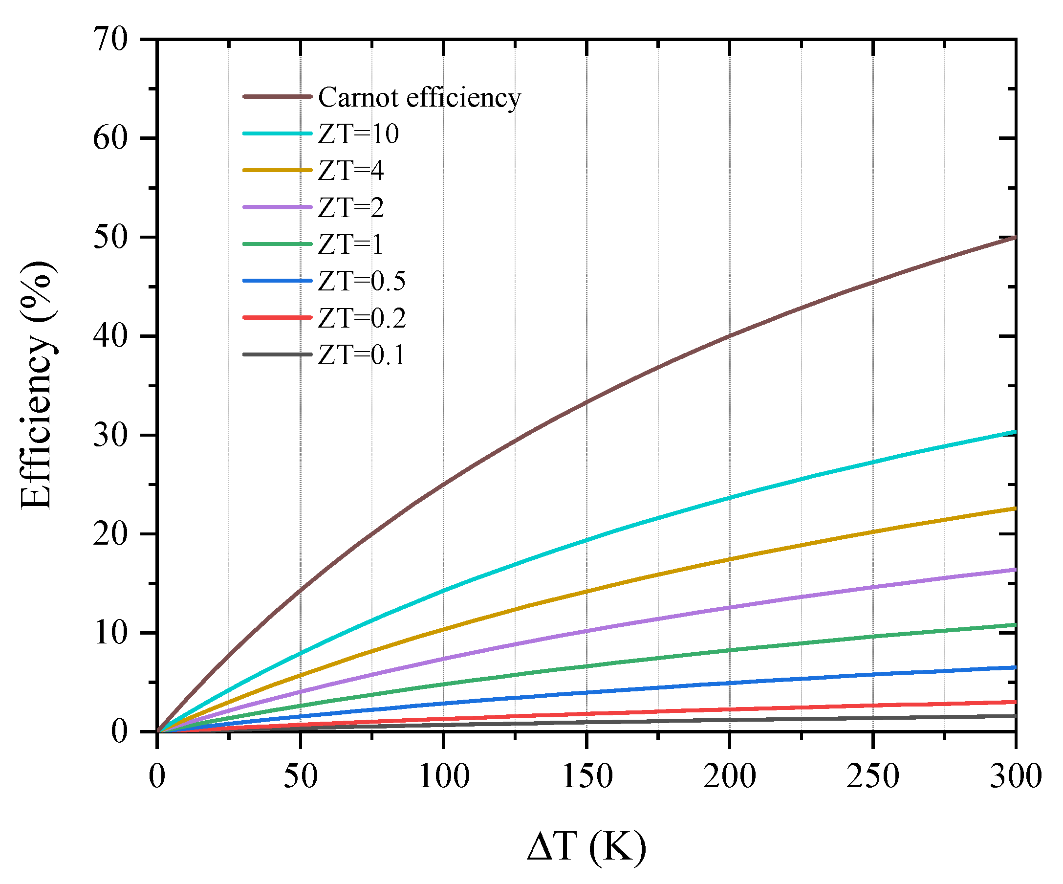
2.2. Thermoelectric Efficiency

Depending on the application, a TE device can perform three functions. If heat is provided, the device can generate electrical power, or, if electrical power is supplied, the device performs cooling or heating. Notice that a thermoelectric generator (TEG) is a heat engine and obeys the laws of thermodynamics [4]. Unfortunately, TEGs are not being used everywhere because of their low conversion efficiency ( η ) for power generation, defined by Equation (2) [4,14,15] as:
η = T H T C T H · 1 + Z T ¯ 1 1 + Z T ¯ + T C T H
where, Z T is the figure of merit (FOM) with average temperatures ( T ¯ ) of the hot side ( T H ) and cold side ( T C ), respectively. Such equation is valid only for an ideal device that effectively converts the input heat at the contact with negligible losses. On the other hand, for refrigeration and air conditioning, the coefficient of performance ( C O P ) is defined by Equation (3) [4,14,15] as:
C O P = T C T H T C · 1 + Z T ¯ T C T H 1 + Z T ¯ + 1
Both Equations (2) and (3) are Z T dependent, indicating that the efficiency of both power generation and cooling rely on the efficiency of the TE material. Therefore, the efficiency of TE materials is determined using a dimensionless figure of merit ( Z T ), which is related to the Seebeck coefficient (S), electrical conductivity ( σ ), thermal conductivity ( κ ), and temperature (T) at which these parameters are evaluated. Equation (4) defines Z T [7,13,14] as:
Z T = S 2 σ κ · T
For obtaining a high Z T , the material should have a high S, a high σ , and a low κ . It is worth mentioning that the physical meaning of Z T is an ideal energy conversion efficiency between heat and electricity when a temperature difference of 1 K is given. S and σ are mainly controlled by the carrier concentration. As both parameters are interrelated, the figure of merit can be maximized for semiconductors. Thus, adopted approaches for improving the Z T , such as boosting the power factor ( S 2 σ ) [16,17,18,19], reducing the thermal conductivity [20,21,22,23], and even the application of both [24,25,26], are necessary for the development of TE materials [27,28,29]. Figure 2 shows the Z T evolution as a function of temperature for bulk and nanostructured SiGe [7,27].
The most commonly used materials in commercial and industrial TE modules are those based on tellurium, such as bismuth telluride (Bi 2 Te 3 ) and lead telluride (PbTe) [27,30], as well as SiGe alloys [4,7]. Currently, the highest Z T value on record is close to three. Specifically, Zao et al. reported a maximum Z T of 2.8 [31]. The last report demonstrates the possibility of achieving a high Z T to develop efficient conversion for widespread commercial applications. However, bulk TE materials have encountered a bottleneck in practical applications, such as shape and performance limitations [32]. Thus, the efficiency effective for industrial applications is a few percent, as shown in Figure 3. In recent years, advances in bulk materials have slowed down due to the absence of novel approaches, so research efforts have been promoted for nanostructured thin-film TE material development. An example of such materials are p-type Bi 2 Te 3 /Sb 2 Te 3 superlattices (SLs) [33]. Regarding the thin-film TEGs, it is worth considering their structures, fabrication processes, and materials. For instance, thin films offer benefits for their use, such as lightweight, low cost, and deposition on different substrates types (plastics, glass, and silicon). Thus, based on such aspects, the advantages of thin film TEGs based on Si and Si alloy materials are as follows: simple design, high output power, high conversion efficiency, and compatibility with planar IC technology [30,34]. Nevertheless, their disadvantages are low performance due to high parasitic heat flux through the membrane and difficulties in the package allowing a temperature difference in the plane applied to the chip-like device. Despite these latter issues, TE thin film materials offer the possibility of device integration with on-chip signal conditioning circuitry and MEMS device fabrication. Therefore, modern research efforts are focused on the development of thin film materials with a Z T = 2 to obtain an efficiency higher than 10% [35].
Regarding silicon-based materials, optimally doped bulk silicon possesses a high-power factor of 50–60 μ W/K 2 cm at 300 K [4,36,37]. However, Si doping produces a maximum Z T of 0.15–0.2 at 1100 K because of its high thermal conductivity, which varies between 90 and 30 W/m·K for the 300–1200 K range, respectively. This is why the Si efficiency is very low and insufficient for most TE applications [38,39]. Likewise, SiGe alloys present a maximum Z T of 0.5 (p-type) or 0.9 (n-type) at 1000–1100 K [14,28,30], employed in radioisotope thermoelectric generators (RTGs), which operate optimally at higher temperatures. Therefore, the silicon-based materials must have a reduced thermal conductivity at intermediate temperatures to be considered as candidates for TE applications.

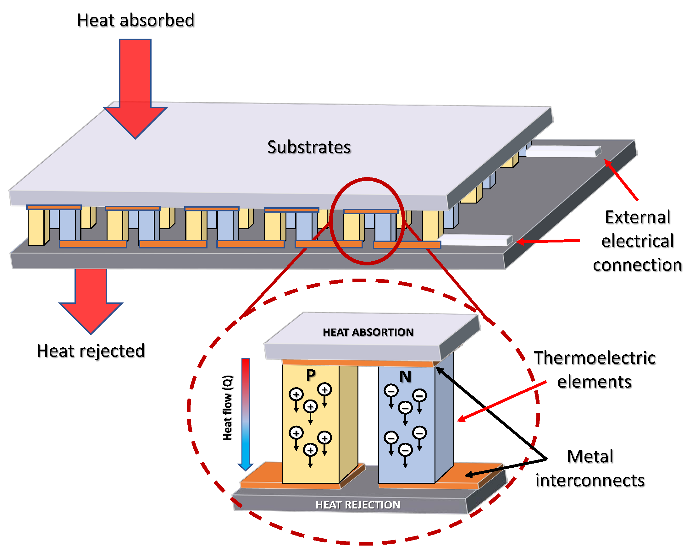
2.3. Thermoelectric Generators (TEGs)

The Seebeck effect is utilized in solid-state devices known as thermoelectric generators (TEGs) to convert thermal energy into electrical energy. A schematic of a TEG device is depicted in Figure 1, where pairs of N-type TE elements (containing free electrons) and P-type TE elements (with free holes) are connected electrically in series and thermally in parallel. A TEG works by utilizing a temperature gradient to transfer heat and power an electrical load through an external circuit. Initially, TEGs were limited to space applications, such as space missions within radioisotope thermoelectric generators (RTGs) to power remote stations because of their low efficiency and high cost [27,40]. However, intensive work has been carried out on the continuous improvement of these devices. Thus, the following advantages [4,27,35] derived from these advances are listed below:
  • Direct energy conversion.
  • No moving parts or working fluids inside the TEG.
  • A long lifetime.
  • No scaling effect.
  • Quiet/silent operation.
  • Adaptable to any workplace.
Therefore, they are ideal for distributed and small power generation, e.g., micro-generation for sensors and microelectronic circuits due to their minimum power levels in which all heat sources are adequate [35]. Furthermore, the field of application extends to emerging technologies, such as thermoelectric energy harvesting, to power low-power systems from ambient temperature differences, which are applied in wireless sensor network (WSN) nodes, the industrial Internet of Things, and wearable electronics [41,42,43]. In recent decades, TEG modules with a size within the range of 1–100 mm 2 and the capacity to deliver 1–1000 μ W of power have been developed through standard micro-fabrication techniques in the microchip industry [30,44]. Features of TEGs, such as tiny dimensions and power generation capabilities, offer the possibility not only to fabricate them with low production costs but also to couple them directly into integrated circuits (ICs) and be able to generate 100–1000 mWh/cm 2 /year (compatible with what power a typical WSN node needs) when placed on hot surfaces. This Makes these TEGs viable options for EH applications [30,45]. In this scenario, TE materials, specifically thin films, are promising candidates due to their capacity of locally converting waste heat into electric energy (regardless of the source of heat) and stability over time [30]. Table 1 shows a classification of the power range that can be harvested by TEGs according to the material’s size and thickness, and the possible field and type of application [46,47,48,49].
According to Table 1, the use of thin film TE materials in TEGs dedicated to heat harvesting and power generation in the nW– μ W range is feasible and useful to meet the energy demands of different applications.

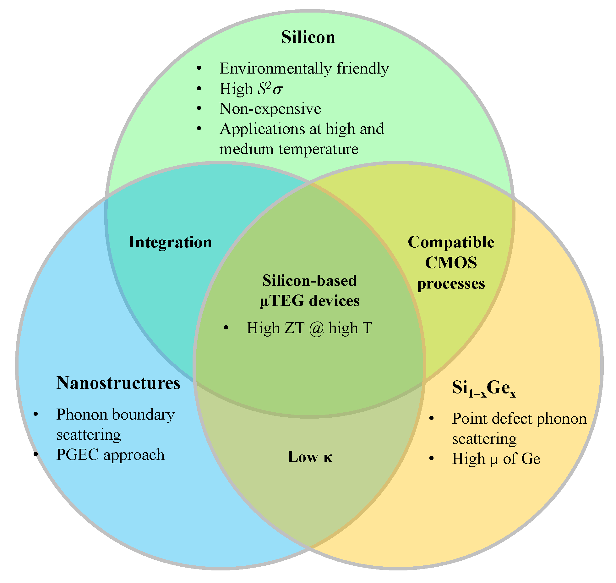
2.4. Silicon-Based Thin Film Materials for TE Power Generation

This review focuses on the study of silicon-based thin film materials for TE power generation. Due to their properties, these materials are excellent candidates for integrated systems applications. It is worth mentioning that Silicon is the second most abundant element in the earth’s crust and, consequently, inexpensive [28,30]. Furthermore, due to its mechanical and chemical properties, and compatibility with CMOS processes [28,30,50], Si has been extensively used not only in the semiconductor industry [51], but also in TE applications [52]. Thus, the well-established knowledge on microfabrication techniques allows Si-based materials an easy integration into TEG and μ TEG devices through conventional CMOS processes [30,53]. Regarding the μ TEG devices, it is important to observe that their compatibility with microfabrication processes is a distinct trait useful for the integration of low-dimensional materials, such as thin films [54,55]. In second place, the main silicon-based TE materials (such as nanostructured silicon and SiGe alloys [28,30,56]) show good prospects for medium to high temperature applications, with a maximum Z T usually ranging from 800 to 1200 K. On the other hand, Si-based materials must have a reduced thermal conductivity and/or optimized power factor for being considered as candidates for TE applications. This means that Si-based materials should implement strategies to reduce their lattice thermal conductivity ( κ l ) through alloying-based approaches and nanostructuration. Meanwhile, for the TE power factor, it is necessary to enhance the electrical conductivity ( σ ) and/or Seebeck coefficient (S).
Finally, a summary of the highlighted features and applied strategies for improving the Z T of silicon-based materials is shown in Figure 4. For instance, silicon technology (including CMOS-MEMS processes) has feasible fabrication methods to produce TEGs at small-scale dimensions (from micro to nanometers) [53]. In conclusion, silicon-based nanostructured materials are promising TEG device candidates for moderate to high temperature applications.

3. ZT Optimization of TE Materials for Power Generation

The research and development of TE materials began by optimizing the compositions, structures, and carrier concentrations, as well as the synthesis processes of many tellurium-based compounds, including BiTe and PbTe, as well as SiGe alloy in the 1950s [57,58,59]. However, Z T had not exceeded unity until the 1990s, when Skutterudites were developed and reached a Z T value of 1.4 for bulk materials [59]. On the other hand, research efforts on organic polymeric materials have been intensified towards the development of portable devices since 1999 [60,61]. However, since the last decade, efforts to improve Z T have used approaches such as nano-structuration (low-dimensional materials in the order of 1–100 nm) applied to bulk materials, as well as the development of thin films with superstructures. The goal is to increase the power factor ( S 2 σ ) or to reduce the thermal conductivity ( κ ) without affecting the electron transport properties [28,30,50,62].

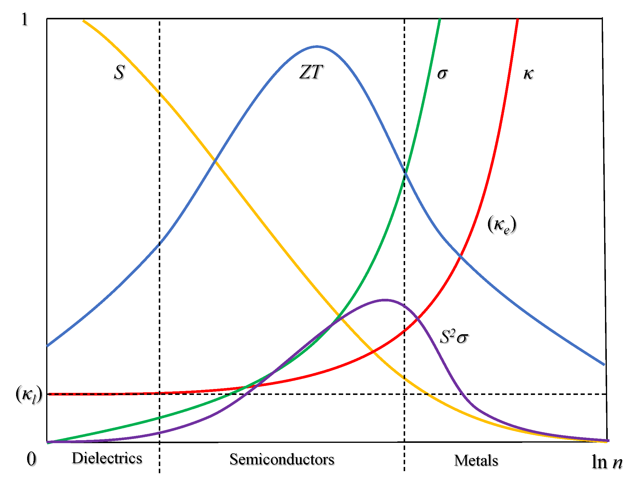
3.1. Challenges in Improving ZT

As mentioned above, TE technology is versatile, has a long service life, and is environmentally friendly since it does not release by-products (waste) into the environment. TE devices are commonly used for cooling or heating (when electrical power is provided), but their use for electrical power generation (when heat is supplied) is still under intensive research. This is due to the low conversion efficiency ( η ) for power generation, defined above in Equation (2), since the conversion factor is less than 1, which is intrinsically dependent on the figure of merit ( Z T ). Furthermore, the electrical and thermal conductivities ( σ and κ , respectively), together with the Seebeck coefficient (S) are considered independent of temperature. Obviously, the higher the Z T , the higher the η . However, improving Z T has been a major challenge since the TE properties (S, σ , and κ ) are interdependent. That is, one cannot be controlled without affecting the other two. Therefore, Z T has not been increased by more than 1.0 until the last few decades. A common way to enhance Z T is changing the carrier concentration (n) to increase the power factor ( S 2 σ ), as shown in Figure 5. An alternative is introducing scattering centers to the material, leading to a reduction in the lattice thermal conductivity ( κ l ).
It is known that S can be defined as the energy difference between the average energy of the carrier mobility, and the Fermi energy [63]. If n increases, both energy levels increase. However, the Fermi energy increases at a faster rate than the average energy, resulting in a net reduction of the Seebeck coefficient, and S 2 σ decreases rapidly. In addition, for most homogeneous materials, n increases σ but reduces S. Therefore, in degenerate metals and semiconductors, S can be expressed as Equation (5) [62,64,65]:
S = 8 π 2 k B 2 3 e h 2 m * T π 3 n 2 3
where m * is the density of effective mass states, e is the electron charge, and k B and h are Boltzmann’s and Planck’s constants, respectively. According to Equation (5), the high value of m * influences the increase of S 2 σ . Most materials that have a high m * generally exhibit a low mobility ( μ ), limiting the power factor by a weighted mobility with the power factor ratio proportional to ( m * ) 3 / 2 μ . It is worth mentioning that there is no optimal effective mass [62,65]. There are conductors with high m * and low μ such as oxides and chalcogenides, as well as semiconductors with low m * and high μ such as SiGe and GaAs [66,67]. In addition, it is known that defects scatter both phonons and electrons. Therefore, there are inherent carrier mobility trade-offs when designing the reduction in the lattice thermal conductivity ( κ l ). Hence, the ratio μ / κ l conditions the Z T enhancement [45], although the increase in such a ratio is usually experimentally obtained by further reduction in κ l , instead of the increase in μ . According to the Wiedemann–Franz law, the electronic contribution to the thermal conductivity is proportional to the material’s electrical conductivity, with a ratio κ e / σ = L T , where L is the Lorentz factor for free electrons. This relationship varies with carrier concentration. Meanwhile, σ depends on the mobility, the carrier concentration, and electronic charge, as σ = μ n e . Moreover, the electronic thermal conductivity ( κ e ) has a dependence given by Equation (6):
κ e = σ L T = μ n e L T
Equation (6) shows that low carrier concentration results in lower electrical conductivity and a reduction in Z T . In conclusion, according to Equations (5) and (6), trying to increase S will increase κ e , contributing to the thermal conductivity, since κ = κ l + κ e . These were the main research challenges in bulk material properties for several decades. However, subsequent efforts were focused on reducing the κ l by phonon engineering applied to bulk and low-dimensional materials, to counteract the increase in κ e [10,62,68,69,70]. The lattice thermal conductivity can be denoted by Equation (7) as:
κ l = 1 3 c v v S λ p h
where c v is the heat capacity, v S is the speed of sound, and λ p h is the mean free path of the phonons. According to the Equation (7), the electronic structure does not determine κ l . Therefore, enhancing Z T can be accomplished as long as κ l is minimized. In addition to decreasing the thermal conductivity, another criterion for achieving ZT∼1 is that the material must achieve minimum values of important parameters such as S∼150 μ V/K. It does not matter whether the material possesses the lowest κ l [6,27,44,64]. The Seebeck coefficient is within the range of 1–10 μ V/K and 10 2 10 3 μ V/K for metals and semiconductors, respectively. Heavily doped semiconductors generally possess good Z T . Therefore, TE materials form a large family that includes semimetals, semiconductors, and ceramics with diverse crystalline forms ranging from single crystals to polycrystals to nanocomposites, and covers different sizes (or shapes) encompassing bulk materials, thin films, nanowires, or agglomerates [26,28,30,62]. In conclusion, it can be stated that the optimization of Z T for TE materials is not as straightforward and simple as Equation (4) and Figure 5 would lead us to think. The interdependence between diverse Z T parameters represents a research challenge, requiring a precise trade-off between material properties [71,72] if a high Z T value is to be achieved. This is because Z T factors are intrinsically and simultaneously dependent on the electronic and the phonon transport processes [73,74,75]. Nonetheless, maximizing TE power and electrical conductivity, while minimizing the thermal conductivity, is crucial to achieve the highest Z T . Regarding this requirement, the best thermoelectric materials have been synthetically defined as a phonon glass electron crystal (PGEC), which suggests that an ideal TE material should be the combination of the thermal conductivity of a glass (or material with disordered structure) and the electronic properties of a crystal [24,66,67,76]. Recent and future research will aim to complement both approaches and thereby achieve materials that possess the best features of disordered and crystalline materials.

3.2. Strategies to Improve ZT

3.2.1. Power Factor Enhancement

Researchers have been searching for new materials with higher Z T to improve the TE power factor. One of the strategies employed is the enhancement of the TE power factor by elevating the Seebeck coefficient (S), as evidenced in previous studies [65,77,78]. For this aim, energy filtering has been utilized whereby nanoscale barriers and nanoinclusions selectively permit the passage of high-energy carriers while restricting low-energy ones [79]. This results in the preferential scattering of low-energy electrons at grain boundaries, leading to an improvement in S since low-energy carriers negatively affect S while high-energy ones contribute more towards S. The energy filter implementation allows an increase in S while keeping σ virtually unchanged [80,81,82]. Conversely, the TE power factor can be enhanced by increasing σ through heavy doping of (∼ 10 19 10 21 cm 3 ), which leads to a reduction in mobility ( μ ) of charge carriers due to the increased ionized impurity scattering [83]. Meanwhile, to balance the trade-off between n and μ , modulation doping can be utilized to discretize the charge carriers of ionized dopants, which reduces ionized impurity scattering for high μ while improving n in TE materials [84].
On the other hand, materials with disordered structures, including amorphous, microcrystalline, and nanocrystalline, have been developed for Si and Si alloys that exhibit attractive properties for TE applications [85]. In the last decade, progress has been observed in improving σ of these disordered atomic structure materials, as shown in Figure 6, aimed at enhancing the TE power factor of Si-based materials. These materials are being explored for their potential as TE materials due to their intrinsic properties, such as low κ and medium/high S. According to the PGEC approach, a material that combines the properties of a crystal (excellent charge transport properties) and an amorphous material (low thermal conductivity) can serve as a highly efficient TE material.

3.2.2. Thermal Conductivity Reduction

Reducing thermal conductivity ( κ ) is critical for enhancing Z T , but it is not a simple optimization process. Nanostructuration has been proposed as a method for significantly reducing κ and improving Z T . According to Equation (4), such a strategy will be successful whether κ decreases, while σ and S are not adversely affected. Notice that κ includes contributions from both electronic ( κ e ) and lattice ( κ l ), with κ e related to σ through the Wiedemann–Franz law given in Equation (6). In SiGe alloys, κ l predominantly contributes to κ rather than κ e [4,62,100], and the reduction in κ l can be achieved by scattering via different types of mesoscale, nano, or atomic defects [101,102,103] or particles [104,105,106,107], provided that their size is smaller than the mean free path (MFP) of heat-carrying phonons in SiGe [108,109,110]. Phonons have a range of wavelengths and contribute differently to the effective heat conduction. Mid-wavelength phonons, with MFPs in the 5–100 nm range, contribute about half of the κ l in Si, while the rest is contributed almost equally by phonon modes in the high (>100 nm) and low (<5 nm) MFP spectrum [111].
Theories and experiments have demonstrated that low-dimensional nanometer-sized structures and bulk materials with nanograins can significantly reduce κ through interface and boundary phonon scattering mechanisms [112,113,114]. Recent advances in one-dimensional nanotubes and nanowires and two-dimensional superstructures, such as Si, SiGe, SiGe/Si, and nanocomposites, have demonstrated an increase in interface phonon scattering, leading to a reduction in κ l [114,115,116]. Figure 7 illustrates that the thickness reduction of Si-based nanostructured materials leads to a decrease in thermal conductivity, resulting in a decrease of up to two orders of magnitude from the κ of crystalline Si (∼100 W/m·K) [4,7,30].
Regarding the disordered structure materials, Nolas and Goldsmid [67] have suggested that amorphous structures may exhibit higher Z T values than crystalline materials whether the MFP of the heat carriers (or vibrons [113]) is shorter than that of the electrons (or holes). This has been demonstrated in several silicon-based semiconductors with amorphous and nanocrystalline structures that possess low κ [21,125,131] and, therefore, may exhibit high Z T values if combined with a large S and high σ [132].
In summary, the reduction in thermal conductivity through effective phonon scattering at the interfaces of superstructures or grain boundaries in nanostructures is the key factor leading to a significant enhancement of Z T in these material systems.

4. Recent Advances in Si-Based Materials for TE Power Generation

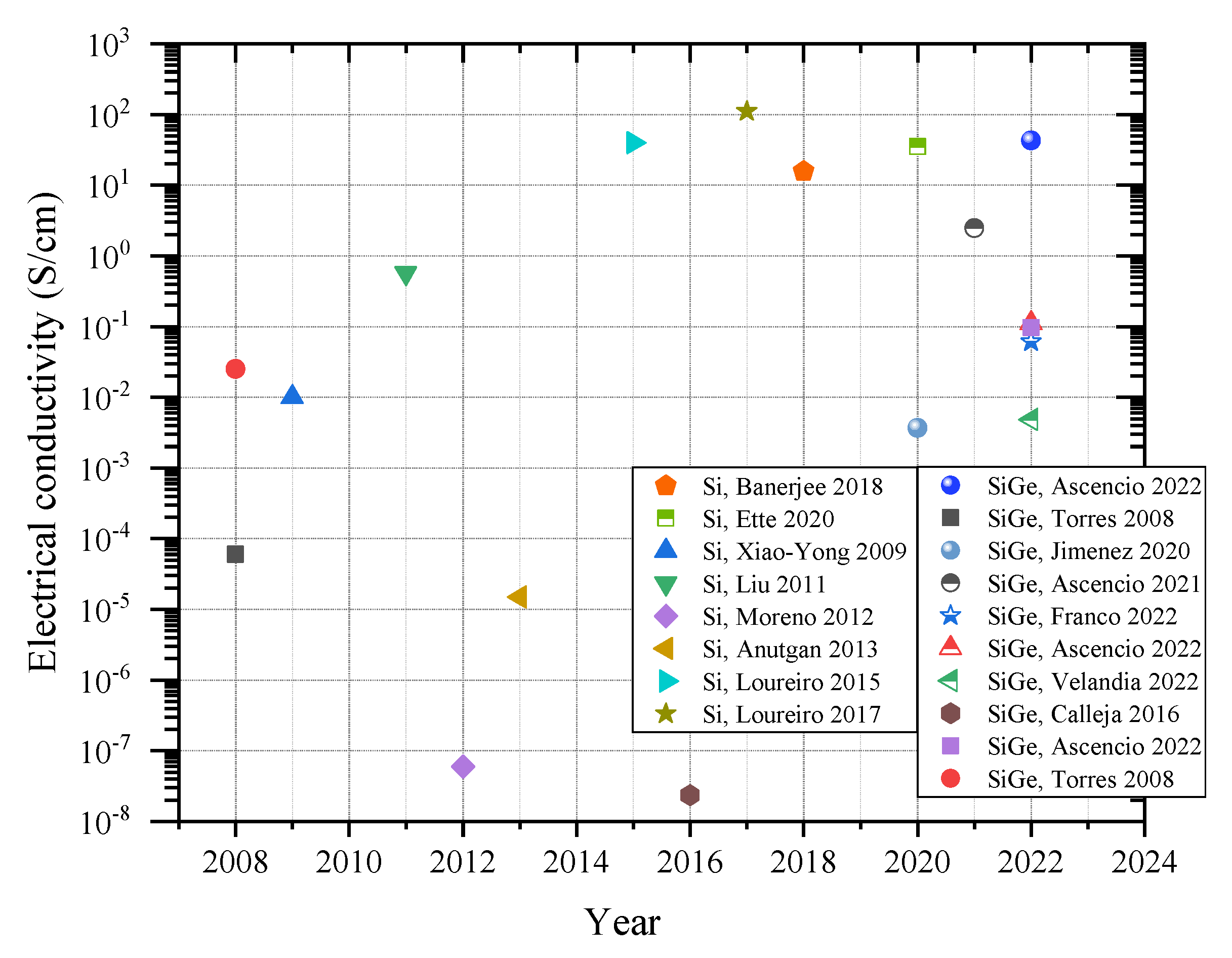
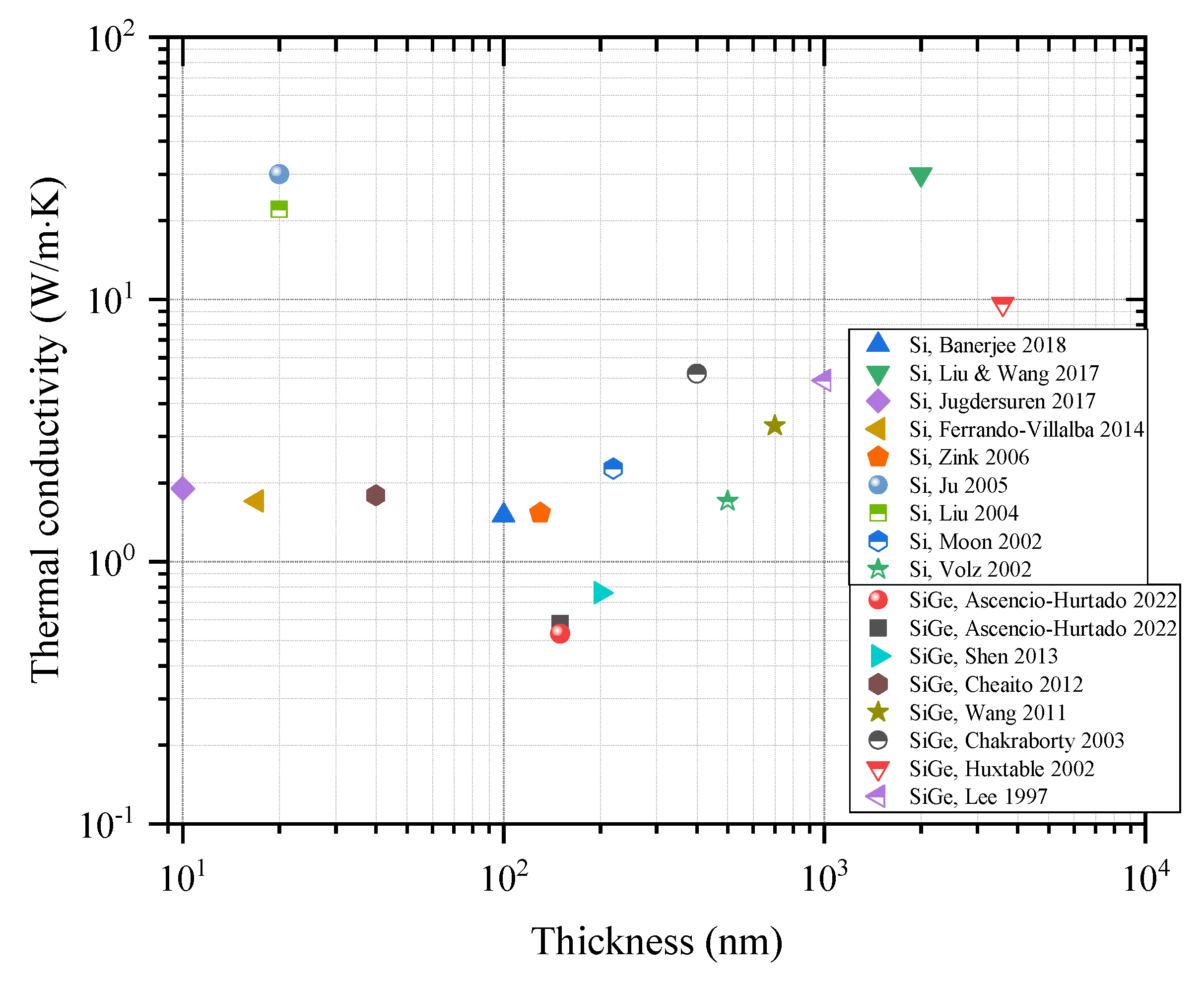
4.1. Deposition Methods for Si-Based Thin Film Materials

The deposition method plays a crucial role in the synthesis and production of nanostructured materials, with their properties being largely determined by the specific deposition conditions employed. The selection of an appropriate deposition technique, therefore, becomes a critical factor in the fabrication of TE materials that exhibit high efficiency, low cost, and reproducibility on a large scale. The current section focuses on elucidating the different deposition methods utilized for the synthesis of Si-based TE materials.
Nanocomposites can be synthesized by combining various nanoparticle preparation and bottom-up assembly techniques, including spark plasma sintering and hot-pressing, which are popular bottom-up methods. Hot-pressing (HP), which is a pressure-assisted sintering process where samples are heated using a direct or alternating current, has become a mature technique for producing TE nanocomposites with elevated Z T values reported in the last decade [4,115]. Additionally, a combination of ball-milling (BM) and HP has been employed to fabricate TE composites such as SiGe alloys [103,104,105]. For instance, the combination of BM and HP has shown remarkable success in improving the TE efficiency of p-type SiGe nanocomposites, with a maximum Z T value of 0.95 recorded at 900–950 °C [133]. In contrast, n-type SiGe nanocomposites achieved a Z T value of 1.3 at 900 °C [134]. In particular, an interesting variant for a large quantity of nanoparticle production is high-energy ball milling (HEBM). Although some grain growth may occur during HP, the grain sizes in the nanocomposites remain in the nanometer range. This approach is appealing from both commercial and research perspectives since it allows for the fast preparation of many TE materials with varying chemical compositions and doping levels, including SiGe alloys with high TE efficiency [106,109]. In the same way, the chemical synthesis and spark plasma sintering (SPS) method is a technique utilized to create certain nanocomposites. This approach starts by synthesizing TE nanoparticles using a chemical process to tune their shape, size distribution, and quality [114,135]. SPS is another pressure-assisted sintering process that employs a pulsed DC to create spark discharges for heating samples under high pressure. In this regard, SiGe alloys have been the primary TE materials in power generation devices that operate within the temperature range of 600–1000 °C [105,107,109]. Despite the positive outcomes obtained, it is worth mentioning that the regulation of impurities during the deposition process is a significant challenge and/or limitation of the BM and HP methods [114,115]. This directly affects the material properties. For instance, impurities (including oxygen and moisture) can significantly impact the material’s electrical conductivity, which results in thermal conductivity and Z T reduction. Therefore, impurities must be removed from the deposition process to ensure the generation of TE materials with the desired properties.
On the other hand, PECVD (plasma-enhanced chemical vapor deposition) is a widely used technique in industries such as microelectronics, photovoltaics, and displays to deposit thin films [95,97,136]. The PECVD process involves plasma generation through an electrical field at a reduced pressure. Plasma is a mixture of electrons, ions, and neutral species. Compared to LP-CVD (500–650 °C) and thermal CVD (800–1200 °C), the advantage of PECVD is the employment of plasma at lower temperatures (T < 300 °C), which results in materials whose properties depend on various deposition conditions such as frequency, pressure, power density, substrate temperature, and gas precursor ratio. Hydrogenated amorphous silicon (a-Si:H) and silicon-germanium (a-SiGe:H) films prepared via PECVD with silane (SiH 4 ), hydrogen (H 2 ), and germane (GeH 4 ), respectively, possess low density-of-state (DOS) films due to hydrogen incorporation in the amorphous lattice [88,89,90,91]. PECVD also allows for material doping via adjustment of precursor gases such as phosphine (PH 3 ) [24,92] and diborane (B 2 H 6 ) [93,99], and LF-PECVD facilitates the production of nanocrystals into the amorphous matrix via high pressure and large hydrogen dilution during the deposition process [95,137,138]. Finally, it is worth mentioning that a fundamental aspect that enables the use of the PECVD technique for thin film deposition is its compatibility with Si-CMOS technology for large scale fabrication and coupling with Si-based TE materials [10,24,136].

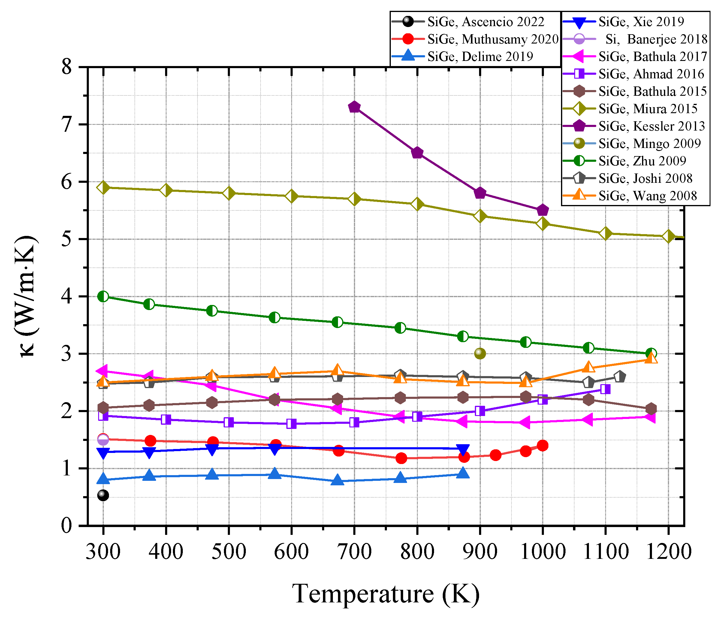
4.2. Evaluation of Thermal Conductivity

This section presents an assessment of the temperature-dependent behavior of thermal conductivity in Si and SiGe thin films, produced by employing the aforementioned approach to optimize their TE properties.
Nanostructuring is an effective method for reducing the thermal conductivity of Si-based thin film materials, as discussed in Section 3.2.2. This study analyzes the nanostructuration method, which involves introducing coherent nanophase boundaries within the TE material to significantly reduce κ without sacrificing S or σ , leading to improved Z T values for SiGe alloys [104,105,107,109,133,139]. In other terms, thermal conductivity reduction is achieved by creating interfaces using nanoinclusions, such as nanoparticles or nano-scale defects, which scatter the phonons over a wide wavelength range. Likewise, SiGe composites scatter short wavelength phonons through point defects caused by alloying [108]. For example, Bathula et al. [107] reported a substantial decrease in κ due to the inclusion of SiC nanoparticles into the SiGe alloy, where phonon scattering is primarily governed by the SiC particles. As a result, the temperature dependence of κ for SiGe is almost constant due to phonon scattering by SiC particles, as shown by the pink curve in Figure 8. Moreover, the lattice mismatch between SiGe alloy and SiC nanoparticles leads to a difference in lattice parameters that affects phonon transmission, resulting in a further reduction in κ .
At elevated temperatures, the thermal conductivity of materials can be influenced by the bipolar effect ( κ b i ), which arises from electron-hole excitation [105]. Conversely, in nanocomposites, the scattering of charge carriers occurs primarily due to acoustic phonons [109]. For instance, the κ of the pink curve [107], orange curve [134], purple curve [104], and red curve [105] in Figure 8 tends to increase for temperatures above 800 K. Such trending is attributed to the κ b i contribution. Nonetheless, there is no significant κ increase that counteracts the action of the phonon scattering caused by nanostructuration.Therefore, it is concluded that the reduction in the contributions of κ l , κ e , and κ b i is observed due to the phonon scattering caused by the coupling of nanostructures in thin film materials. Consequently, κ exhibits limited variability over a temperature range of 300–1200 K.

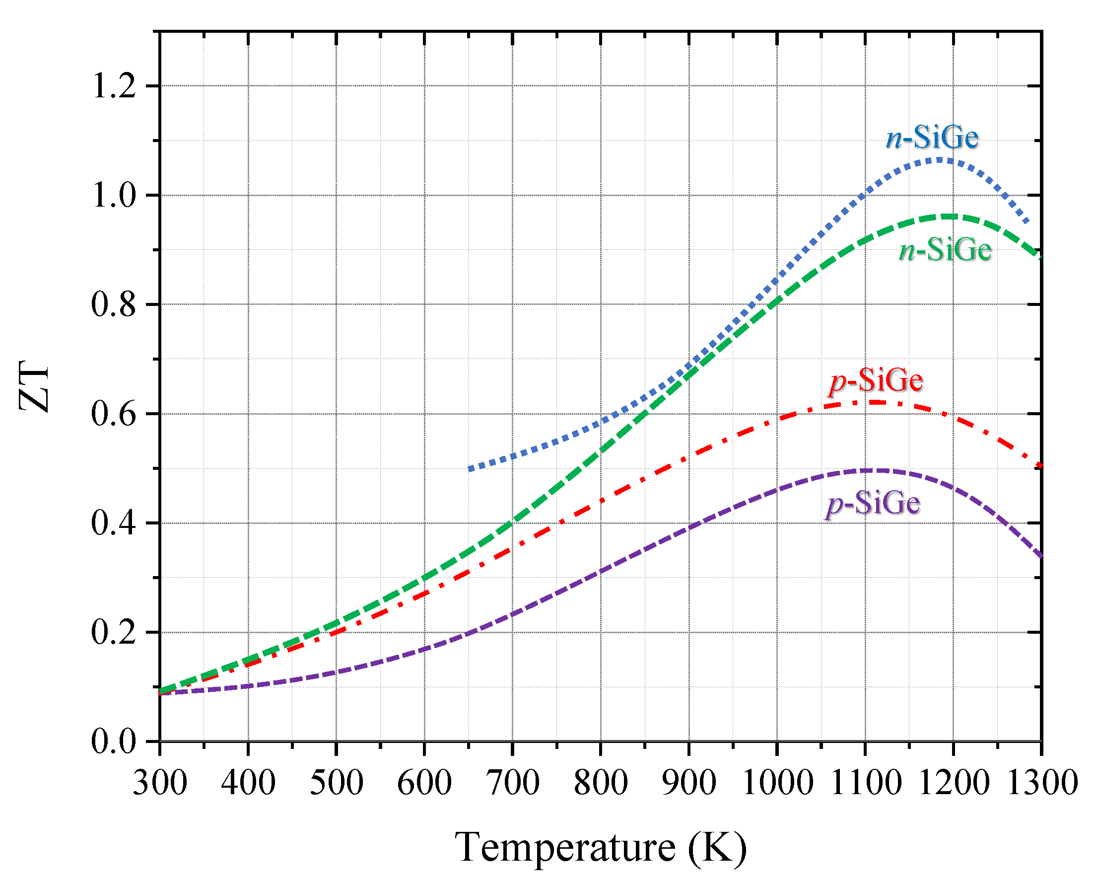
4.3. State-of-the-Art of Si-Based Thin Films Materials
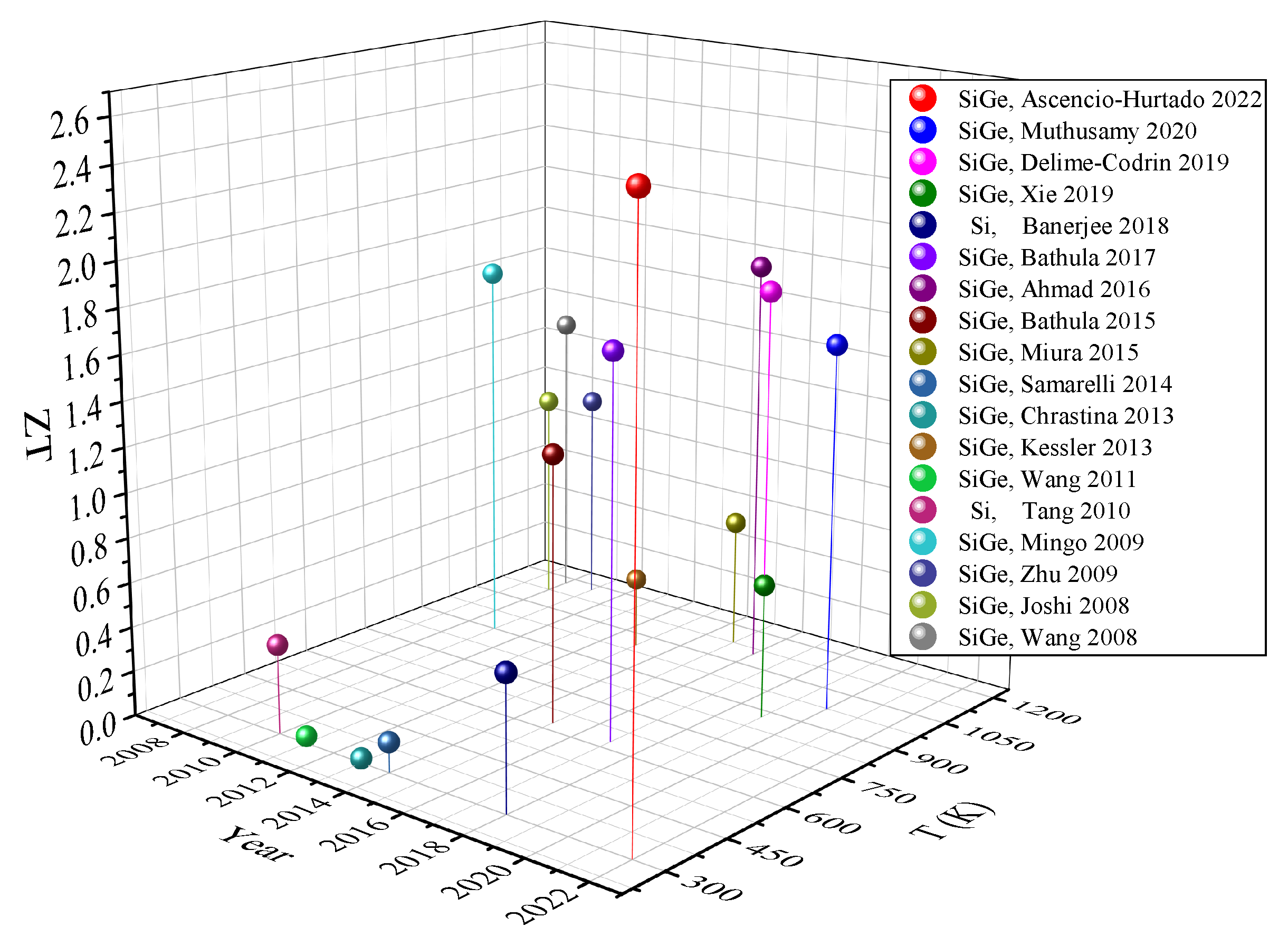
Many research groups have adopted the use of nanostructuring as a strategy to enhance the TE bulk properties of existing materials, such as silicon-based composites or alloys. With advances in characterization and manufacturing techniques, a more sophisticated understanding of materials and their properties has been achieved. Recent work on various nanostructures shows that silicon-based materials hold great potential for the development of TE power generation devices operating at moderate and high temperatures. The compatibility of Si with conventional micro and nano-scale manufacturing technologies creates the attractive possibility of fully integrated TE energy harvesting systems. This is summarized in Figure 4. Thus, some pieces of research that report the improvement of TE efficiency under the nanostructuring approach are described below.
Z. Wang et al. [127] reported the optimization of a polycrystalline silicon germanium (poly-SiGe) material by phosphorus doping for its use in thermal energy harvesting. The poly-SiGe film doping was carried out by the implantation method with phosphorus ions. The calculation of the Z T value at room temperature yielded a value of 0.032, given a κ of 3.3 W/m·K for the material. Chrastina et al. [140] reported on the use of SiGe heterostructures with multiple quantum wells (MQW) stacks grown by low-energy chemical vapor deposition (LE-CVD) to achieve a κ in the range of 10–20 W/m·K and with a Seebeck coefficient of 200 μ V/K. However, this only yielded a Z T of 0.01–0.02. In order to achieve a large FOM, it is necessary to increase S 2 σ while reducing κ to improve Z T . As evidence, Ahmad et al. [104], in their study, employed yttrium silicide (YSi 2 ) metal nanoparticles to enhance the performance of P-type SiGe alloy. The nanoinclusions form coherent interfaces with the SiGe matrix, leading to a reduction in the grain size of SiGe and a strong suppression of κ (∼2.38 W/m·K) without affecting the S 2 σ . The improved performance resulted in a high Z T of 1.81 at 1100 K, while the SiGe-YSi 2 nanocomposites also exhibited an enhancement in mechanical toughness.
On the other hand, disordered structure materials have shown promising advances in the optimization of their TE properties for use as TE materials by exploiting their low κ and high S. Thus, researchers have focused on improving the electrical conductivity ( σ ) by incorporating N-type doping. Banerjee et al. [20] have utilized a low-pressure chemical vapor deposition (LPCVD) technique to deposit a-Si thin films on P-type c-Si substrate at 560 °C, achieving a Z T of 0.64 at 300 K. The authors attribute this success to the inclusion of arsenic ion implantation for N-type doping, followed by low-temperature activation of the dopant through annealing at 525 °C for 20 min. Eventually, Ascencio-Hurtado et al. [24] reported on the discovery of the nc-SiGeH material, which exhibits a high Z T value of 2.61 at room temperature. This was achieved by depositing thin films of phosphorus-doped nc-SiGeH using the LF-PECVD technique, followed by thermal treatment at 500 °C to activate the dopant, promote hydrogen effusion, and reduce structural defects (such as dangling bonds) to improve charge carrier transport. The nc-SiGeH thin films are formed of an amorphous matrix and a crystalline fraction, leading to two competing mechanisms that influence their electrical conductivity. In other terms, the optimization of Z T was accomplished by improving S 2 σ through N-type doping and thermal annealing, while the lowest thermal conductivity was attained by maintaining the amorphous phase of the material. According to Beyer et al. [141], the impact of annealing on the σ and S is substantial under specific conditions. Specifically, the increase in σ can be attributed to the hopping of charge carriers through energy states near to the Fermi level. Concerning the reduction in κ , one plausible explanation is that heat transfer in amorphous materials is predominantly dominated by localized lattice vibrations [125]. These vibrations possess a minimal MFP, generally less than 1 A ˚ , which can be attributed to the structural disorder of amorphous solids as per theoretical and numerical studies on thermal transport [70,142]. Consequently, the nc-SiGeH material features a coexistence of amorphous and crystalline phases, which is essential for achieving optimal characteristics from both phases according to the PGEC approach for waste heat recovery applications. The findings of the research show that the significant rise in Z T for disordered structure materials is mainly due to the improvement in electrical conductivity through doping while keeping the amorphous state of Si and SiGe films to preserve the thermal conductivity and Seebeck coefficient at the desired level.
In conclusion, the successful utilization of thin film materials for TE applications requires a significant reduction in κ , without any compromise on the Seebeck coefficient or electrical conductivity, which leads to a substantial improvement in the Z T . A summary of the Z T results for thin films of silicon-based materials is presented in Figure 9 and Table 2.
From the data collected, it is demonstrated that silicon-based materials are a viable option for energy harvesting applications.
Figure 8. Evaluation of thermal conductivity versus temperature for Si and SiGe thin films [20,24,103,104,105,106,107,108,109,133,134,139,143,144].
Eng 04 00082 g008
Figure 9. Z T for Si and SiGe thin films over the last 15 years [20,21,24,85,103,104,105,106,107,108,109,127,133,134,139,140,143,144].
Eng 04 00082 g009
Table 2. Summary of Z T values for Si and SiGe thin films.
YearMaterialTypeTemperature (K)ZTReference
2022SiGeN3002.61Ascencio-Hurtado et al. [24]
2020SiGeP9731.63Muthusamy et al. [105]
2019SiGeN8731.88Delime-Codrin et al. [106]
2019SiGeN8730.60Xie et al. [143]
2018SiN3000.60Banerjee et al. [20]
2017SiGe6271.70Bathula et al. [107]
2016SiGeP11001.81Ahmad et al. [104]
2015SiGe6271.20Bathula et al. [109]
2015SiGeN11250.58Miura et al. [139]
2014SiGe3000.13Samarelli et al. [85]
2013SiGe3000.02Chrastina et al. [140]
2013SiGeP10000.32Kessler et al. [144]
2011SiGeN3000.03Wang et al. [127]
2010Si3000.40Tang et al. [21]
2009SiGe9001.70Mingo et al. [108]
2009SiGeN11750.95Zhu et al. [103]
2008SiGeP11230.95Joshi et al. [133]
2008SiGeN11731.30Wang et al. [134]

4.4. Thin Film TEG Devices

Over the last two decades, there has been a notable focus on micro thermoelectric generators ( μ TEGs), which have become increasingly popular due to their small size and high output voltage, resulting from the advancements in microelectromechanical systems (MEMS) technology [34]. Compared to bulk TEGs, thin-film or μ TEGs operate at low-temperature differences. These devices can provide a stable electrical power supply to miniature electronic instruments, which is crucial for emerging technologies development such as the Internet of Things (IoT), smart cities, wearable electronics, and wireless sensor networks that rely on waste heat recovery [34]. For instance, the Matrix Powerwatch II, a smartwatch that runs on body heat, includes a step counter, sleep tracker, and calorie counter among its features [145]. On the other hand, it has been observed that film Si-based materials have great potential for use in TEG devices from the progress in Z T enhancement. Moreover, the compatibility of these materials with CMOS processes makes the fabrication of TEG devices at micro- and nanometer dimensions an affordable possibility to address the needs of emerging technologies [28,34]. Thin film TEGs can be categorized into three distinct structural types. The first, Class-A, or a vertical structure, is defined by its out-of-plane design. Meanwhile, Class-B, known as a lateral structure, is distinguished by its planar geometry. Lastly, Class-C, a hybrid structure, is characterized by its combination of vertical heat flow and lateral current flow. The current state-of-the-art in μ TEG devices utilizing thin film materials based on silicon is presented in Table 3. The μ TEG devices compiled herein and based on thin film materials use hybrid, lateral, and vertical architectures. Furthermore, several situations and conclusions are deduced from the compilation made. However, only two are briefly described and discussed below.
First, the number of published articles on μ TEGs is relatively lower than those on macroscopic TEGs. This disparity can be attributed to the challenges in fabricating and integrating conventional TE material nanostructures into devices. Although this may have an impact on processing costs and mass production, μ TEGs can still generate sufficient power in the range of μ W–mW to power low-power electronic devices. Furthermore, μ TEGs offer the possibility of exploring alternative applications beyond energy harvesting for which these devices are the optimal solution. Therefore, technological challenges related to the microelectronic integration of low-dimensional materials, such as thin films, must be addressed to further advance this area of research [28,30,112]. Finally, it is worth mentioning that power density, a commonly used metric for comparing the efficiency of macroscopic commercial modules, may not be suitable for accurately assessing the performance of microdevices in real-world operating environments, particularly when temperature gradients are imposed [30]. Nevertheless, the power density of a device with integrated nanostructures is a useful metric for assessing its electronic efficiency, but only when its thickness is considered. In addition, most of the devices listed in Table 3) use conventional microfabrication techniques, making them promising candidates for wasted heat recovery applications.

5. Overview and Prospective

Over the last 15 years, there has been significant progress in improving the efficiency of TE materials and developing μ TEGs to meet the low-power needs of emerging technologies, such as the IoT. Notice that such devices provide a μ W–mW range of power, which is sufficient to power energy-efficient devices. The primary reason behind this progress has been the Z T enhancement of TE materials due to the incorporation of nanostructures into the material. Among these, Si-based thin film materials have been extensively researched and regarded as potential candidates. In other terms, recent work on both crystalline and disordered-structure Si-based materials has demonstrated that they can be useful in practical μ TEG applications. Conversely, to the best of our knowledge, there are no devices that include silicide nanostructures documented in the literature. In the forthcoming years, it is expected that more research will be carried out on silicon-based TE nanomaterials, focusing on both materials’ characterization and TEG system integration, which is now feasible due to established technologies. Notice that μ TEG devices are capable of providing energy to low-power consumption devices in the μ W–mW power range. Furthermore, the advantages of abundant raw materials and mass production through CMOS processes make Si-based materials competitive for energy harvesting applications. Additionally, the ease with which silicon-based TE nanomaterials can be microfabricated to co-integrate with other small-scale electronics or MEMS devices makes them well suited for such a purpose. This suggests that the exploration of coupling these materials with MEMS-based microdevices and sensors will continue in the near future.
In summary, the present review article provides an overview of the recent progress in the fabrication and device integration of Si-based materials for TE energy harvesting applications. The aim is to present state-of-the-art TE materials through a compilation of work research done on thin-film Si and SiGe materials. Additionally, this work serves as a reference to position the progress, challenges, and possibilities of Si-based thin film device development. While previous reviews have predominantly focused on large-scale power conversion using bulk and Te-based materials, this review emphasizes the extensive research efforts towards the development of innovative and cost-effective thin-film Si-based devices for harnessing wasted energy as heat in the nW–mW range.

Author Contributions

Conceptualization, C.R.A.-H., R.C.A.L., J.J.E.-L. and A.T.J.; investigation, C.R.A.-H., R.C.A.L., J.J.E.-L. and A.T.J.; writing—original draft preparation, C.R.A.-H.; writing—review and editing, C.R.A.-H., R.C.A.L., J.J.E.-L. and A.T.J.; supervision, C.R.A.-H., R.C.A.L., J.J.E.-L. and A.T.J. All authors have read and agreed to the published version of the manuscript.

Funding

This research received no external funding.

Institutional Review Board Statement

Not applicable.

Informed Consent Statement

Not applicable.

Data Availability Statement

Not applicable.

Acknowledgments

C.R.A.-H. expresses his gratitude to the Mexican National Council for Science and Technology (CONACyT) for its support through the program: Estancias Posdoctorales por México 2022.

Conflicts of Interest

The authors declare no conflict of interest.

Abbreviations

The following abbreviations are used in this manuscript:
TEThermoelectric
TEGThermoelectric generator
FOMFigure of merit
EHEnergy harvesting
SiGeSilicon-germanium
PECVDPlasma-enhanced chemical vapor deposition
PGECPhonon-glass electron-crystal
MFPMean free path
CMOSComplementary metal-oxide semiconductor

References

  1. Ali, M.B.; Saidur, R.; Hossain, M.S. A review on emission analysis in cement industries. Renew. Sustain. Energy Rev. 2011, 15, 2252–2261. [Google Scholar] [CrossRef]
  2. Xi, H.; Luo, L.; Fraisse, G. Development and applications of solar-based thermoelectric technologies. Renew. Sustain. Energy Rev. 2007, 11, 923–936. [Google Scholar] [CrossRef]
  3. Thirugnanasambandam, M.; Iniyan, S.; Goic, R. A review of solar thermal technologies. Renew. Sustain. Energy Rev. 2010, 14, 312–322. [Google Scholar] [CrossRef]
  4. Rowe, D.M. Thermoelectrics Handbook: Micro to Nano; CRC Press: Boca Raton, FL, USA, 2018. [Google Scholar]
  5. Soin, N. Chapter 10—Magnetic Nanoparticles—Piezoelectric Polymer Nanocomposites for Energy Harvesting. In Micro and Nano Technologies; El-Gendy, A.A., Barandiarán, J.M., Hadimani, R.L.B.T.-M.N.M., Eds.; Elsevier: Amsterdam, The Netherlands, 2018; pp. 295–322. [Google Scholar] [CrossRef]
  6. Zheng, J. Recent advances on thermoelectric materials. Front. Phys. 2008, 3, 269–279. [Google Scholar] [CrossRef]
  7. Tritt, T.M. Thermoelectric Phenomena, Materials, and Applications. Annu. Rev. Mater. Res. 2011, 41, 433–448. [Google Scholar] [CrossRef]
  8. Paul, D. Thermoelectric Energy Harvesting. In ICT—Energy—Concepts towards Zero; Fagas, G., Gammaitoni, L., Paul, D., Berini, G.A., Eds.; IntechOpen: Rijeka, Croatia, 2014. [Google Scholar] [CrossRef]
  9. Radousky, H.B.; Liang, H. Energy Harvesting: An Integrated View of Materials, Devices and Applications. Nanotechnology 2012, 23, 502001. [Google Scholar] [CrossRef]
  10. Nandihalli, N.; Gregory, D.H.; Mori, T. Energy-Saving Pathways for Thermoelectric Nanomaterial Synthesis: Hydrothermal/Solvothermal, Microwave-Assisted, Solution-Based, and Powder Processing. Adv. Sci. 2022, 25, 2106052. [Google Scholar] [CrossRef]
  11. Paradiso, J.A.; Starner, T. Energy scavenging for mobile and wireless electronics. IEEE Pervasive Comput. 2005, 4, 18–27. [Google Scholar] [CrossRef]
  12. Vedernikov, M.V.; Iordanishvili, E.K.A.F. Ioffe and origin of modern semiconductor thermoelectric energy conversion. In Proceedings of the Seventeenth International Conference on Thermoelectrics, Proceedings ICT98 (Cat. No.98TH8365), Nagoya, Japan, 28 May 1998; pp. 37–42. [Google Scholar] [CrossRef]
  13. Ioffe, A.F. Semiconductor Thermoelements and Thermoelectric Cooling; Infosearch Ltd.: London, UK, 1957. [Google Scholar]
  14. Snyder, G.J.; Toberer, E.S. Complex Thermoelectric Materials. Nat. Mater. 2008, 7, 105–114. [Google Scholar] [CrossRef]
  15. Kim, H.S.; Liu, W.; Chen, G.; Chu, C.-W.; Ren, Z. Relationship between thermoelectric figure of merit and energy conversion efficiency. Proc. Natl. Acad. Sci. USA 2015, 112, 8205–8210. [Google Scholar] [CrossRef]
  16. Ferrando-Villalba, P.; Lopeandía, A.F.; Alvarez, F.X.; Paul, B.; de Tomás, C.; Alonso, M.I.; Garriga, M.; Goñi, A.R.; Santiso, J.; Garcia, G.; et al. Tailoring Thermal Conductivity by Engineering Compositional Gradients in Si1-xGex superlattices. Nano Res. 2015, 8, 2833–2841. [Google Scholar] [CrossRef]
  17. Qiu, B.; Chen, G.; Tian, Z. Effects of Aperiodicity and Roughness on Coherent Heat Conduction in Superlattices. Nanoscale Microscale Thermophys. Eng. 2015, 19, 272–278. [Google Scholar] [CrossRef]
  18. Kang, H.; Li, J.; Liu, Y.; Guo, E.; Chen, Z.; Liu, D.; Fan, G.; Zhang, Y.; Jiang, X.; Wang, T. Optimizing the thermoelectric transport properties of BiCuSeO via doping with the rare-earth variable-valence element Yb. J. Mater. Chem. C 2018, 6, 8479–8487. [Google Scholar] [CrossRef]
  19. Yang, S.H.; Zhu, T.J.; Sun, T.; He, J.; Zhang, S.N.; Zhao, X.B. Nanostructures in High-Performance (GeTe)x(AgSbTe2)100-Xthermoelectric Materials. Nanotechnology 2008, 19, 245707. [Google Scholar] [CrossRef]
  20. Banerjee, D.; Vallin, Ö.; Samani, K.M.; Majee, S.; Zhang, S.L.; Liu, J.; Zhang, Z.B. Elevated Thermoelectric Figure of Merit of N-Type Amorphous Silicon by Efficient Electrical Doping Process. Nano Energy 2018, 44, 89–94. [Google Scholar] [CrossRef]
  21. Tang, J.; Wang, H.-T.; Lee, D.H.; Fardy, M.; Huo, Z.; Russell, T.P.; Yang, P. Holey Silicon as an Efficient Thermoelectric Material. Nano Lett. 2010, 10, 4279–4283. [Google Scholar] [CrossRef]
  22. Lee, E.K.; Yin, L.; Lee, Y.; Lee, J.W.; Lee, S.J.; Lee, J.; Cha, S.N.; Whang, D.; Hwang, G.S.; Hippalgaonkar, K.; et al. Large Thermoelectric Figure-of-Merits from SiGe Nanowires by Simultaneously Measuring Electrical and Thermal Transport Properties. Nano Lett. 2012, 12, 2918–2923. [Google Scholar] [CrossRef]
  23. Markussen, T. Surface Disordered Ge–Si Core–Shell Nanowires as Efficient Thermoelectric Materials. Nano Lett. 2012, 12, 4698–4704. [Google Scholar] [CrossRef]
  24. Ascencio-Hurtado, C.R.; Torres, A.; Ambrosio, R.; Moreno, M.; Álvarez-Quintana, J.; Hurtado-Macías, A. N-type amorphous silicon-germanium thin films with embedded nanocrystals as a novel thermoelectric material of elevated ZT. J. Alloys Compd. 2022, 890, 161843. [Google Scholar] [CrossRef]
  25. Beekman, M.; Morelli, D.T.; Nolas, G.S. Better thermoelectrics through glass-like crystals. Nat. Mater. 2015, 14, 1182–1185. [Google Scholar] [CrossRef]
  26. Singh, D.; Ahuja, R. Dimensionality effects in high-performance thermoelectric materials: Computational and experimental progress in energy harvesting applications. WIREs Comput. Mol. Sci. 2022, 12, e1547. [Google Scholar] [CrossRef]
  27. He, J.; Tritt, T.M. Advances in thermoelectric materials research: Looking back and moving forward. Science 2017, 357, eaak9997. [Google Scholar] [CrossRef] [PubMed]
  28. Basu, R.; Singh, A. High temperature Si–Ge alloy towards thermoelectric applications: A comprehensive review. Mater. Today Phys. 2021, 21, 100468. [Google Scholar] [CrossRef]
  29. Vineis, C.J.; Shakouri, A.; Majumdar, A.; Kanatzidis, M.G. Nanostructured Thermoelectrics: Big Efficiency Gains from Small Features. J. Adv. Mater. 2010, 22, 3970–3980. [Google Scholar] [CrossRef] [PubMed]
  30. Gadea, G.; Pacios, M.; Morata, Á.; Tarancón, A. Silicon-based nanostructures for integrated thermoelectric generators. J. Phys. D 2018, 51, 423001. [Google Scholar] [CrossRef]
  31. Chang, C.; Wu, M.; He, D.; Pei, Y.; Wu, C.-F.; Wu, X.; Yu, H.; Zhu, F.; Wang, K.; Chen, Y.; et al. 3D charge and 2D phonon transports leading to high out-of-plane ZT in n-type SnSe crystals. Science 2018, 360, 778–783. [Google Scholar] [CrossRef]
  32. Chen, X.; Dai, W.; Wu, T.; Luo, W.; Yang, J.; Jiang, W.; Wang, L. Thin Film Thermoelectric Materials: Classification, Characterization, and Potential for Wearable Applications. Coatings 2018, 8, 244. [Google Scholar] [CrossRef]
  33. Chen, X.; Zhou, Z.; Lin, Y.-H.; Nan, C. Thermoelectric thin films: Promising strategies and related mechanism on boosting energy conversion performance. J. Mater. 2020, 6, 494–512. [Google Scholar] [CrossRef]
  34. Yan, J.; Liao, X.; Yan, D.; Chen, Y. Review of Micro Thermoelectric Generator. J. Microelectromech. Syst. 2018, 27, 1–18. [Google Scholar] [CrossRef]
  35. Champier, D. Thermoelectric generators: A review of applications. Energy Convers. Manag. 2017, 140, 167–181. [Google Scholar] [CrossRef]
  36. Schierning, G. Silicon nanostructures for thermoelectric devices: A review of the current state of the art. Phys. Status Solidi A 2014, 211, 1235–1249. [Google Scholar] [CrossRef]
  37. Overhof, H.; Thomas, P. Electronic Transport in Hydrogenated Amorphous Semiconductors; Springer: Berlin/Heidelberg, Germany, 1989. [Google Scholar]
  38. Ohishi, Y.; Xie, J.; Miyazaki, Y.; Aikebaier, Y.; Muta, H.; Kurosaki, K.; Yamanaka, S.; Uchida, N.; Tada, T. Thermoelectric properties of heavily boron- and phosphorus-doped silicon. J. Appl. Phys. 2015, 54, 71301. [Google Scholar] [CrossRef]
  39. Stranz, A.; Kähler, J.; Waag, A.; Peiner, E. Thermoelectric Properties of High-Doped Silicon from Room Temperature to 900 K. J. Electron. Mater. 2013, 42, 2381–2387. [Google Scholar] [CrossRef]
  40. He, W.; Zhang, G.; Zhang, X.; Ji, J.; Li, G.; Zhao, X. Recent Development and Application of Thermoelectric Generator and Cooler. Appl. Energy 2015, 143, 1–25. [Google Scholar] [CrossRef]
  41. Stark, I. Micro Thermoelectric Generators. In Micro Energy Harvesting; John Wiley & Sons, Ltd.: Hoboken, NJ, USA, 2015; pp. 245–269. [Google Scholar] [CrossRef]
  42. Son, D.; Lee, J.; Qiao, S.; Ghaffari, R.; Kim, J.; Lee, J.E.; Song, C.; Kim, S.J.; Lee, D.J.; Jun, S.W.; et al. Multifunctional wearable devices for diagnosis and therapy of movement disorders. Nat. Nanotechnol. 2014, 9, 397–404. [Google Scholar] [CrossRef] [PubMed]
  43. Bahk, J.-H.; Fang, H.; Yazawa, K.; Shakouri, A. Flexible thermoelectric materials and device optimization for wearable energy harvesting. J. Mater. Chem. C. 2015, 3, 10362–10374. [Google Scholar] [CrossRef]
  44. Briand, D.; Yeatman, E.; Roundy, S. Micro Energy Harvesting; Wiley Online Library: Hoboken, NJ, USA, 2015. [Google Scholar]
  45. Snyder, G.J. Small Thermoelectric Generators. J. Electrochem. Soc. 2008, 17, 54. [Google Scholar] [CrossRef]
  46. Siddique, A.R.M.; Mahmud, S.; Heyst, B.V. A review of the state of the science on wearable thermoelectric power generators (TEGs) and their existing challenges. Renew. Sustain. Energy Rev. 2017, 73, 730–744. [Google Scholar] [CrossRef]
  47. Koplow, M.; Chen, A.; Steingart, D.; Wright, P.K.; Evans, J.W. Thick film thermoelectric energy harvesting systems for biomedical applications. In Proceedings of the 2008 5th International Summer School and Symposium on Medical Devices and Biosensors, Hong Kong, China, 1–3 June 2008; pp. 322–325. [Google Scholar] [CrossRef]
  48. Perez-Marín, A.P.; Lopeandía, A.F.; Abad, L.; Ferrando-Villaba, P.; Garcia, G.; Lopez, A.M.; Muñoz-Pascual, F.X.; Rodríguez-Viejo, J. Micropower thermoelectric generator from thin Si membranes. Nano Energy 2014, 4, 73–80. [Google Scholar] [CrossRef]
  49. Wijngaards, D.D.L. Lateral on-Chip Integrated Peltier Elements: Based on Polycrystalline Silicon-Germanium; Technische Universiteit Delft: Delft, The Netherlands, 2003. [Google Scholar]
  50. Donmez Noyan, I.; Gadea, G.; Salleras, M.; Pacios, M.; Calaza, C.; Stranz, A.; Dolcet, M.; Morata, A.; Tarancon, A.; Fonseca, L. SiGe Nanowire Arrays Based Thermoelectric Microgenerator. Nano Energy 2019, 57, 492–499. [Google Scholar] [CrossRef]
  51. Newman, R.C. A review of the growth and structure of thin films of germanium and silicon. Microelectron. Reliab. 1964, 3, 121–138. [Google Scholar] [CrossRef]
  52. Steele, M.C.; Rosi, F.D. Thermal Conductivity and Thermoelectric Power of Germanium-Silicon Alloys. J. Appl. Phys. 1958, 29, 1517–1520. [Google Scholar] [CrossRef]
  53. Jaziri, N.; Boughamoura, A.; Müller, J.; Mezghani, B.; Tounsi, F.; Ismail, M. A comprehensive review of Thermoelectric Generators: Technologies and common applications. Energy Rep. 2020, 6, 264–287. [Google Scholar] [CrossRef]
  54. Ziouche, K.; Yuan, Z.; Lejeune, P.; Lasri, T.; Leclercq, D.; Bougrioua, Z. Silicon-Based Monolithic Planar Micro Thermoelectric Generator Using Bonding Technology. J. Microelectromech. Syst. 2017, 26, 45–47. [Google Scholar] [CrossRef]
  55. Chen, Y.-W.; Wu, C.-C.; Hsu, C.-C.; Dai, C.-L. Fabrication and Testing of Thermoelectric CMOS-MEMS Microgenerators with CNCs Film. Appl. Sci. 2018, 8, 1047. [Google Scholar] [CrossRef]
  56. Nozariasbmarz, A.; Agarwal, A.; Coutant, Z.A.; Hall, M.J.; Liu, J.; Liu, R.; Malhotra, A.; Norouzzadeh, P.; Öztürk, M.C.; Ramesh, V.P.; et al. Thermoelectric Silicides: A Review. Jpn. J. Appl. Phys. 2017, 56, 05DA04. [Google Scholar] [CrossRef]
  57. Shinohara, Y.; Umezawa, O.; Martínez, L.; Kharissova, O.; Kharisov, B. Thermoelectric Power Generation from Waste Heat; Springer: Cham, Switzerland, 2018; pp. 1–19. [Google Scholar] [CrossRef]
  58. Shinohara, Y. Recent progress of thermoelectric devices or modules in Japan. Mater. Today Proc. 2017, 4, 12333–12342. [Google Scholar] [CrossRef]
  59. Kajikawa, T.; Ohta, T.; Nishida, I.A.; Matsuura, K.; Natsubara, K. Overview of Thermoelectric Conversion Systems, 1995.
  60. Nandihalli, N.; Liu, C.-J.; Mori, T. Polymer based thermoelectric nanocomposite materials and devices: Fabrication and characteristics. Nano Energy 2020, 78, 105186. [Google Scholar] [CrossRef]
  61. Petsagkourakis, I.; Tybrandt, K.; Crispin, X.; Ohkubo, I.; Satoh, N.; Mori, T. Thermoelectric materials and applications for energy harvesting power generation. Sci. Technol. Adv. 2018, 19, 836–862. [Google Scholar] [CrossRef]
  62. Alam, H.; Ramakrishna, S. A Review on the Enhancement of Figure of Merit from Bulk to Nano-Thermoelectric Materials. Nano Energy 2013, 2, 190–212. [Google Scholar] [CrossRef]
  63. Pichanusakorn, P.; Bandaru, P. Nanostructured thermoelectrics. Mater. Sci. Eng. R Rep. 2010, 67, 19–63. [Google Scholar] [CrossRef]
  64. Suwardi, A.; Bash, D.; Ng, H.K.; Gomez, J.R.; Repaka, D.V.M.; Kumar, P.; Hippalgaonkar, K. Inertial effective mass as an effective descriptor for thermoelectrics via data-driven evaluation. J. Mater. Chem. A 2019, 17, 23762–23769. [Google Scholar] [CrossRef]
  65. Huang, Z.; Wang, D.; Li, C.; Wang, J.; Wang, G.; Zhao, L.-D. Improving the thermoelectric performance of p-type PbSe via synergistically enhancing the Seebeck coefficient and reducing electronic thermal conductivity. J. Mater. Chem. A 2020, 8, 4931–4937. [Google Scholar] [CrossRef]
  66. Slack, G.A.; Rowe, D.M. CRC Handbook of Thermoelectrics; CRC Press: Boca Raton, FL, USA, 1995. [Google Scholar]
  67. Nolas, G.S.; Goldsmid, H.J. The Figure of Merit in Amorphous Thermoelectrics. Phys. Status Solidi A 2002, 194, 271–276. [Google Scholar] [CrossRef]
  68. Satyala, N.; Tahmasbi Rad, A.; Zamanipour, Z.; Norouzzadeh, P.; Krasinski, J.S.; Tayebi, L.; Vashaee, D. Reduction of Thermal Conductivity of Bulk Nanostructured Bismuth Telluride Composites Embedded with Silicon Nano-Inclusions. J. Appl. Phys. 2014, 115, 44304. [Google Scholar] [CrossRef]
  69. Chen, G.; Zhou, S.; Yao, D.-Y.; Kim, C.; Zheng, X.; Liu, Z.; Wang, K. Heat conduction in alloy-based superlattices. In Proceedings of the Seventeenth International Conference on Thermoelectrics, Proceedings ICT98, Nagoya, Japan, 28 May 1998; Volume 28, pp. 202–205. [Google Scholar] [CrossRef]
  70. Norouzzadeh, P.; Nozariasbmarz, A.; Krasinski, J.S.; Vashaee, D. Thermal Conductivity of Nanostructured SixGe1-x in Amorphous Limit by Molecular Dynamics Simulation. J. Appl. Phys. 2015, 117, 214303. [Google Scholar] [CrossRef]
  71. Wudil, Y.; Gondal, M.; Almessiere, M.; Alsayoud, A. The multi-dimensional approach to synergistically improve the performance of inorganic thermoelectric materials: A critical review. Arab. J. Chem. 2021, 14, 103103. [Google Scholar] [CrossRef]
  72. Xiao, C.; Li, Z.; Li, K.; Huang, P.; Xie, Y. Decoupling Interrelated Parameters for Designing High Performance Thermoelectric Materials. Acc. Chem. Res. 2014, 47, 1287–1295. [Google Scholar] [CrossRef]
  73. Qiu, W.; He, H.; Wang, Z.; Hu, Q.; Cui, X.; Wang, Z.; Zhang, Y.; Gu, L.; Yang, L.; Sun, Y.; et al. Enhancing the figure of merit of n-type PbTe materials through multi-scale graphene induced interfacial engineering. Nano Today 2021, 39, 101176. [Google Scholar] [CrossRef]
  74. Baker, J.L.; Park, C.; Kenney-Benson, C.; Sharma, V.K.; Kanchana, V.; Vaitheeswaran, G.; Pickard, C.J.; Cornelius, A.; Velisavljevic, N.; Kumar, R.S. Pressure-Induced Enhancement of Thermoelectric Figure of Merit and Structural Phase Transition in TiNiSn. J. Phys. Chem. Lett. 2021, 12, 1046–1051. [Google Scholar] [CrossRef]
  75. Gaidar, G.P. The Effect of Thermal Treatment on the Thermoelectric Figure of Merit of Silicon Doped Using Nuclear Transmutation. Surf. Eng. Appl. Electrochem. 2021, 57, 425–430. [Google Scholar] [CrossRef]
  76. Vaqueiro, P.; Powell, A.V. Recent developments in nanostructured materials for high-performance thermoelectrics. J. Mater. Chem. 2010, 20, 9577–9584. [Google Scholar] [CrossRef]
  77. Heremans, J.P.; Jovovic, V.; Toberer, E.S.; Saramat, A.; Kurosaki, K.; Charoenphakdee, A.; Yamanaka, S.; Snyder, G.J. Enhancement of Thermoelectric Efficiency in PbTe by Distortion of the Electronic Density of States. Science 2008, 321, 554–557. [Google Scholar] [CrossRef] [PubMed]
  78. Xiao, Y.; Zhao, L.-D. Charge and phonon transport in PbTe-based thermoelectric materials. Npj Quantum Mater. 2018, 3, 55. [Google Scholar] [CrossRef]
  79. Singha, A.; Muralidharan, B. Incoherent scattering can favorably influence energy filtering in nanostructured thermoelectrics. Sci. Rep. 2017, 7, 7879. [Google Scholar] [CrossRef]
  80. Hwang, J.-Y.; Kim, J.; Kim, H.-S.; Kim, S.-I.; Lee, K.H.; Kim, S.W. Effect of Dislocation Arrays at Grain Boundaries on Electronic Transport Properties of Bismuth Antimony Telluride: Unified Strategy for High Thermoelectric Performance. Adv. Energy Mater. 2018, 8, 1800065. [Google Scholar] [CrossRef]
  81. Liang, Z.; Boland, M.J.; Butrouna, K.; Strachan, D.R.; Graham, K.R. Increased power factors of organic–inorganic nanocomposite thermoelectric materials and the role of energy filtering. J. Mater. Chem. A 2017, 5, 15891–15900. [Google Scholar] [CrossRef]
  82. Zhang, D.; Lei, J.; Guan, W.; Ma, Z.; Wang, C.; Zhang, L.; Cheng, Z.; Wang, Y. Enhanced thermoelectric performance of BiSbTe alloy: Energy filtering effect of nanoprecipitates and the effect of SiC nanoparticles. J. Alloys Compd. 2019, 784, 1276–1283. [Google Scholar] [CrossRef]
  83. Zhang, X.; Pei, Y. Manipulation of charge transport in thermoelectrics. Npj Quantum Mater. 2017, 2, 68. [Google Scholar] [CrossRef]
  84. Weidner, M.; Fuchs, A.; Bayer, T.J.M.; Rachut, K.; Schnell, P.; Deyu, G.K.; Klein, A. Defect Modulation Doping. Adv. Funct. Mater. 2017, 29, 1807906. [Google Scholar] [CrossRef]
  85. Samarelli, A.; Llin, L.F.; Cecchi, S.; Frigerio, J.; Chrastina, D.; Isella, G.; Gubler, E.M.; Etzelstorfer, T.; Stangl, J.; Zhang, Y.; et al. Prospects for SiGe thermoelectric generators. Solid-State Electron. 2014, 98, 70–74. [Google Scholar] [CrossRef]
  86. Gao, X.-Y.; Zhao, J.-T.; Liu, Y.-F.; Lin, Q.-G.; Chen, Y.-S.; Gu, J.-H.; Yang, S.-E.; Lu, J.-X. Characterized Microstructure and Electrical Properties of Hydrogenated Nanocrystalline Silicon Films by Raman and Electrical Conductivity Spectra. Acta Phys. Pol. A 2009, 115, 738–741. [Google Scholar]
  87. Liu, S.; Zeng, X.; Peng, W.; Xiao, H.; Yao, W.; Xie, X.; Wang, C.; Wang, Z. Improvement of Amorphous Silicon N-i-p Solar Cells by Incorporating Double-Layer Hydrogenated Nanocrystalline Silicon Structure. J. Non-Cryst. Solids 2011, 357, 121–125. [Google Scholar] [CrossRef]
  88. Moreno, M.; Torres, A.; Ambrosio, R.; Torres, E.; Rosales, P.; Zuñiga, C.; Reyes-Betanzo, C.; Calleja, W.; De La Hidalga, J.; Monfil, K. Study of Polymorphous Silicon as Thermo-Sensing Film for Infrared Detectors. Mater. Sci. Eng. B Solid-State Mater. Adv. Technol. 2012, 177, 756–761. [Google Scholar] [CrossRef]
  89. Anutgan, T.; Uysal, S. Low Temperature Plasma Production of Hydrogenated Nanocrystalline Silicon Thin Films. Curr. Appl. Phys. 2013, 13, 181–188. [Google Scholar] [CrossRef]
  90. Loureiro, J.; Mateus, T.; Filonovich, S.; Ferreira, M.; Figueira, J.; Rodrigues, A.; Donovan, B.F.; Hopkins, P.E.; Ferreira, I. Hydrogenated Nanocrystalline Silicon Thin Films with Promising Thermoelectric Properties. Appl. Phys. A 2015, 120, 1497–1502. [Google Scholar] [CrossRef]
  91. Loureiro, J.; Mateus, T.; Filonovich, S.; Ferreira, M.; Figueira, J.; Rodrigues, A.; Donovan, B.F.; Hopkins, P.E.; Ferreira, I. Improved Thermoelectric Properties of Nanocrystalline Hydrogenated Silicon Thin Films by Post-Deposition Thermal Annealing. Thin Solid Film. 2017, 642, 276–280. [Google Scholar] [CrossRef]
  92. Ette, P.M.; Bhargav, P.B.; Ahmed, N.; Chandra, B.; Rayarfrancis, A.; Ramesha, K. Nanocrystalline Silicon Embedded Highly Conducting Phosphorus Doped Silicon Thin Film as High Power Lithium Ion Battery Anode. Electrochim. Acta 2020, 330, 135318. [Google Scholar] [CrossRef]
  93. Torres, A.; Moreno, M.; Kosarev, A.; Heredia, A. Thermo-Sensing Silicon-Germanium-Boron Films Prepared by Plasma for Un-Cooled Micro-Bolometers. J. Non-Cryst. Solids 2008, 354, 2556–2560. [Google Scholar] [CrossRef]
  94. Calleja, C.; Torres, A.; Moreno, M.; Rosales, P.; Sanz-Pascual, M.T.; Velázquez, M. A Microbolometer Fabrication Process Using Polymorphous Silicon–Germanium Films (Pm-SixGey:H) as Thermosensing Material. Phys. Status Solidi A 2016, 213, 1864–1868. [Google Scholar] [CrossRef]
  95. Jimenez, R.; Moreno, M.; Torres, A.; Ambrosio, R.; Heredia, A.; Ponce, A. Reduction of Residual Stress in Polymorphous Silicon Germanium Films and Their Evaluation in Microbolometers. Eur. Phys. J. Appl. Phys. 2020, 89, 30101. [Google Scholar] [CrossRef]
  96. Ascencio-Hurtado, C.; Torres, A.; Moreno, M.; Ambrosio, R. High Conductivity Intrinsic a-SiGe Films Deposited at Low-Temperature. In Proceedings of the 2021 IEEE Latin America Electron Devices Conference (LAEDC), Cancun, Mexico, 19–21 April 2021; pp. 1–4. [Google Scholar] [CrossRef]
  97. Ascencio-Hurtado, C.R.; Torres, A.; Ambrosio, R.; Moreno, M.; Arenas-Hernández, A. Evaluation of the influence of hydrogen-dilution ratio and doping on the properties of a-SiGe:H films. In Proceedings of the 2022 IEEE Latin American Electron Devices Conference (LAEDC), Cancun, Mexico, 4–6 July 2022; pp. 1–4. [Google Scholar] [CrossRef]
  98. Velandia, O.; Moreno, M.; Zavala, R.; Morales, A.; Torres, A.; Zuñiga, C.; Rosales, P.; Hernández, L.; Carlos, N. Hydrogenated amorphous silicon germanium films doped with nitrogen (a-SiGe:H,N) to improve the long-wave infrared (LWIR) region absorption. In Proceedings of the 2022 IEEE Latin American Electron Devices Conference (LAEDC), Cancun, Mexico, 4–6 July 2022; pp. 1–4. [Google Scholar] [CrossRef]
  99. Franco, E.; Torres, A. High electrical conductivity of P type a-SiGe:H films deposited by PECVD. In Proceedings of the 2022 IEEE Latin American Electron Devices Conference (LAEDC), Cancun, Mexico, 4–6 July 2022; pp. 1–4. [Google Scholar] [CrossRef]
  100. Poudeu, P.F.P.; D’Angelo, J.; Kong, H.; Downey, A.; Short, J.L.; Pcionek, R.; Hogan, T.P.; Uher, C.; Kanatzidis, M.G. Nanostructures versus Solid Solutions: Low Lattice Thermal Conductivity and Enhanced Thermoelectric Figure of Merit in Pb9.6Sb0.2Te10-xSex Bulk Materials. J. Am. Chem. Soc. 2006, 128, 14347–14355. [Google Scholar] [CrossRef] [PubMed]
  101. Bhandari, C.M.; Rowe, D.M. Boundary scattering of phonons. J. Phys. C Solid State Phys. 1978, 11, 1787. [Google Scholar] [CrossRef]
  102. Savvides, N.; Goldsmid, H.J. The effect of boundary scattering on the high-temperature thermal conductivity of silicon. J. Phys. C Solid State Phys. 1973, 6, 1701. [Google Scholar] [CrossRef]
  103. Zhu, G.H.; Lee, H.; Lan, Y.C.; Wang, X.W.; Joshi, G.; Wang, D.Z.; Yang, J.; Vashaee, D.; Guilbert, H.; Pillitteri, A.; et al. Increased Phonon Scattering by Nanograins and Point Defects in Nanostructured Silicon with a Low Concentration of Germanium. Phys. Rev. Lett. 2009, 102, 196803. [Google Scholar] [CrossRef]
  104. Ahmad, S.; Singh, A.; Bohra, A.; Basu, R.; Bhattacharya, S.; Bhatt, R.; Meshram, K.; Roy, M.; Sarkar, S.K.; Hayakawa, Y.; et al. Boosting thermoelectric performance of p-type SiGe alloys through in-situ metallic YSi2 nanoinclusions. Nano Energy 2016, 27, 282–297. [Google Scholar] [CrossRef]
  105. Muthusamy, O.; Ghodke, S.; Singh, S.; Delime-Codrin, K.; Nishino, S.; Adachi, M.; Yamamoto, Y.; Matsunami, M.; Harish, S.; Shimomura, M.; et al. Enhancement of the Thermoelectric Performance of Si-Ge Nanocomposites Containing a Small Amount of Au and Optimization of Boron Doping. J. Electron. Mater. 2020, 49, 2813–2824. [Google Scholar] [CrossRef]
  106. Delime-Codrin, K.; Omprakash, M.; Ghodke, S.; Sobota, R.; Adachi, M.; Kiyama, M.; Matsuura, T.; Yamamoto, Y.; Matsunami, M.; Takeuchi, T. Large figure of merit ZT = 1.88 at 873 K achieved with nanostructured Si0.55Ge0.35(P0.10Fe0.01). Appl. Phys. Express 2019, 12, 45507. [Google Scholar] [CrossRef]
  107. Bathula, S.; Jayasimhadri, M.; Gahtori, B.; Kumar, A.; Srivastava, A.K.; Dhar, A. Enhancement in thermoelectric performance of SiGe nanoalloys dispersed with SiC nanoparticles. Phys. Chem. Chem. Phys. 2017, 19, 25180–25185. [Google Scholar] [CrossRef]
  108. Mingo, N.; Hauser, D.; Kobayashi, N.P.; Plissonnier, M.; Shakouri, A. “Nanoparticle-in-Alloy” Approach to Efficient Thermoelectrics: Silicides in SiGe. Nano Lett. 2009, 9, 711–715. [Google Scholar] [CrossRef]
  109. Bathula, S.; Jayasimhadri, M.; Gahtori, B.; Singh, N.K.; Tyagi, K.; Srivastava, A.K.; Dhar, A. The role of nanoscale defect features in enhancing the thermoelectric performance of p-type nanostructured SiGe alloys. Nanoscale 2015, 7, 12474–12483. [Google Scholar] [CrossRef] [PubMed]
  110. Garg, J.; Bonini, N.; Kozinsky, B.; Marzari, N. Role of Disorder and Anharmonicity in the Thermal Conductivity of Silicon-Germanium Alloys: A First-Principles Study. Phys. Rev. Lett. 2011, 106, 045901. [Google Scholar] [CrossRef] [PubMed]
  111. Bera, C.; Mingo, N.; Volz, S. Marked Effects of Alloying on the Thermal Conductivity of Nanoporous Materials. Phys. Rev. Lett. 2010, 104, 115502. [Google Scholar] [CrossRef] [PubMed]
  112. Giri, K.; Wang, Y.-L.; Chen, T.-H.; Chen, C.-H. Challenges and strategies to optimize the figure of merit: Keeping eyes on thermoelectric metamaterials. Mater. Sci. Semicond. 2022, 150, 106944. [Google Scholar] [CrossRef]
  113. Wingert, M.C.; Zheng, J.; Kwon, S.; Chen, R. Thermal Transport in Amorphous Materials: A Review. Semicond. Sci. Technol. 2016, 31, 113003. [Google Scholar] [CrossRef]
  114. Lan, Y.; Minnich, A.J.; Chen, G.; Ren, Z. Enhancement of Thermoelectric Figure-of-Merit by a Bulk Nanostructuring Approach. Adv. Funct. Mater. 2010, 20, 357–376. [Google Scholar] [CrossRef]
  115. Dresselhaus, M.S.; Chen, G.; Tang, M.Y.; Yang, R.G.; Lee, H.; Wang, D.Z.; Ren, Z.F.; Fleurial, J.-P.; Gogna, P. New Directions for Low-Dimensional Thermoelectric Materials. Adv. Mater. 2007, 19, 1043–1053. [Google Scholar] [CrossRef]
  116. Borca-Tasciuc, T.; Liu, W.; Liu, J.; Zeng, T.; Song, D.W.; Moore, C.D.; Chen, G.; Wang, K.L.; Goorsky, M.S.; Radetic, T.; et al. Thermal Conductivity of Symmetrically Strained Si/Ge Superlattices. Superlattices Microstruct. 2000, 28, 199–206. [Google Scholar] [CrossRef]
  117. Liu, H.; Wang, L. Measurements of thermal conductivity and the coefficient of thermal expansion for polysilicon thin films by using double-clamped beams. J. Micromech. Microeng. 2017, 28, 15010. [Google Scholar] [CrossRef]
  118. Jugdersuren, B.; Kearney, B.T.; Queen, D.R.; Metcalf, T.H.; Culbertson, J.C.; Chervin, C.N.; Stroud, R.M.; Nemeth, W.; Wang, Q.; Liu, X. Thermal conductivity of amorphous and nanocrystalline silicon films prepared by hot-wire chemical-vapor deposition. Phys. Rev. B 2017, 96, 14206. [Google Scholar] [CrossRef]
  119. Ferrando-Villalba, P.; Lopeandia, A.F.; Abad, L.; Llobet, J.; Molina-Ruiz, M.; Garcia, G.; Gerbolès, M.; Alvarez, F.X.; Goñi, A.R.; Muñoz-Pascual, F.J.; et al. In-plane thermal conductivity of sub-20 nm thick suspended mono-crystalline Si layers. Nanotechnology 2014, 25, 185402. [Google Scholar] [CrossRef]
  120. Zink, B.L.; Pietri, R.; Hellman, F. Thermal Conductivity and Specific Heat of Thin-Film Amorphous Silicon. Phys. Rev. Let. 2006, 96, 55902. [Google Scholar] [CrossRef] [PubMed]
  121. Ju, Y.S. Phonon heat transport in silicon nanostructures. Appl. Phys. Lett. 2005, 85, 153106. [Google Scholar] [CrossRef]
  122. Liu, W.; Asheghi, M. Phonon–boundary scattering in ultrathin single-crystal silicon layers. Appl. Phys. Lett. 2004, 84, 3819–3821. [Google Scholar] [CrossRef]
  123. Moon, S.; Hatano, M.; Lee, M.; Grigoropoulos, C.P. Thermal conductivity of amorphous silicon thin films. Int. J. Heat Mass Transf. 2002, 45, 2439–2447. [Google Scholar] [CrossRef]
  124. Volz, S.; Feng, X.; Fuentes, C.; Guérin, P.; Jaouen, M. Thermal Conductivity Measurements of Thin Amorphous Silicon Films by Scanning Thermal Microscopy. Int. J. Thermophys. 2002, 23, 1645–1657. [Google Scholar] [CrossRef]
  125. Shen, B.; Zeng, Z.; Lin, C.; Hu, Z. Thermal Conductivity Measurement of Amorphous Si/SiGe Multilayer Films by 3 Omega Method. Int. J. Therm. Sci. 2013, 66, 19–23. [Google Scholar] [CrossRef]
  126. Cheaito, R.; Duda, J.C.; Beechem, T.E.; Hattar, K.; Ihlefeld, J.F.; Medlin, D.L.; Rodriguez, M.A.; Campion, M.J.; Piekos, E.S.; Hopkins, P.E. Experimental Investigation of Size Effects on the Thermal Conductivity of Silicon-Germanium Alloy Thin Films. Phys. Rev. Lett. 2012, 109, 195901. [Google Scholar] [CrossRef]
  127. Wang, Z.; Su, J.; van Andel, Y.; Nguyen, H.; Vullers, R.J.M. Material optimization of phosphorus-doped polycrystalline silicon germanium for miniaturized thermoelectric generator. In Proceedings of the 2011 16th International Solid-State Sensors, Actuators and Microsystems Conference, Beijing, China, 5–9 June 2011; pp. 346–349. [Google Scholar]
  128. Chakraborty, S.; Kleint, C.A.; Heinrich, A.; Schneider, C.M.; Schumann, J.; Falke, M.; Teichert, S. Thermal Conductivity in Strain Symmetrized Si/Ge Superlattices on Si(111). Appl. Phys. Lett. 2003, 83, 4184–4186. [Google Scholar] [CrossRef]
  129. Huxtable, S.T.; Abramson, A.R.; Tien, C.-L.; Majumdar, A.; LaBounty, C.; Fan, X.; Zeng, G.; Bowers, J.E.; Shakouri, A.; Croke, E.T. Thermal Conductivity of Si/SiGe and SiGe/SiGe Superlattices. Appl. Phys. Lett. 2002, 80, 1737–1739. [Google Scholar] [CrossRef]
  130. Lee, S.-M.; Cahill, D.G.; Venkatasubramanian, R. Thermal Conductivity of Si–Ge Superlattices. Appl. Phys. Lett. 1997, 70, 2957–2959. [Google Scholar] [CrossRef]
  131. Zhan, T.; Xu, Y.; Goto, M.; Tanaka, Y.; Kato, R.; Sasaki, M.; Kagawa, Y. Phonons with Long Mean Free Paths in a-Si and a-Ge. Appl. Phys. Lett. 2014, 104, 71911. [Google Scholar] [CrossRef]
  132. Fitriani; Ovik, R.; Long, B.D.; Barma, M.C.; Riaz, M.; Sabri, M.F.M.; Said, S.M.; Saidur, R. A review on nanostructures of high-temperature thermoelectric materials for waste heat recovery. Renew. Sustain. Energy Rev. 2016, 64, 635–659. [Google Scholar] [CrossRef]
  133. Joshi, G.; Lee, H.; Lan, Y.; Wang, X.; Zhu, G.; Wang, D.; Gould, R.W.; Cuff, D.C.; Tang, M.Y.; Dresselhaus, M.S.; et al. Enhanced Thermoelectric Figure-of-Merit in Nanostructured p-type Silicon Germanium Bulk Alloys. Nano Lett. Am. Chem. Soc. 2008, 8, 4670–4674. [Google Scholar] [CrossRef]
  134. Wang, X.W.; Lee, H.; Lan, Y.C.; Zhu, G.H.; Joshi, G.; Wang, D.Z.; Yang, J.; Muto, A.J.; Tang, M.Y.; Klatsky, J.; et al. Enhanced thermoelectric figure of merit in nanostructured n-type silicon germanium bulk alloy. Appl. Phys. Lett. 2008, 93, 193121. [Google Scholar] [CrossRef]
  135. Murray, C.B.; Kagan, C.R.; Bawendi, M.G. Synthesis and Characterization of Monodisperse Nanocrystals and Close-Packed Nanocrystal Assemblies. Annu. Rev. Mater. Sci. 2000, 30, 545–610. [Google Scholar] [CrossRef]
  136. Cosme, I.; Kosarev, A.; Zarate-Galvez, S.; Martinez, H.E.; Mansurova, S.; Kudriavtsev, Y. Study of Si and Ge Atoms Termination Using H-Dilution in SiGe:H Alloys Deposited by Radio Frequency (13.56 MHz) Plasma Discharge at Low Temperature. Materials 2020, 13, 1045. [Google Scholar] [CrossRef]
  137. Ascencio-Hurtado, C.; Ambrosio, R.; Torres, A.; Moreno, M.; Ponce, A.; Candia-García, F.; Arenas-Hernández, A. Role of nanocrystal incrustation in the electrical conductivity of pm-SiGe:H thin films at room temperature. Mater. Lett. 2023, 342, 134346. [Google Scholar] [CrossRef]
  138. Roca i Cabarrocas, P.; Chaâbane, N.; Kharchenko, A.V.; Tchakarov, S. Polymorphous silicon thin films produced in dusty plasmas: Application to solar cells. Plasma Phys. Control Fusion 2004, 46, B235–B243. [Google Scholar] [CrossRef]
  139. Miura, A.; Zhou, S.; Nozaki, T.; Shiomi, J. Crystalline-Amorphous Silicon Nanocomposites with Reduced Thermal Conductivity for Bulk Thermoelectrics. ACS Appl. Mater. Interfaces 2015, 7, 13484–13489. [Google Scholar] [CrossRef]
  140. Chrastina, D.; Cecchi, S.; Hague, J.P.; Frigerio, J.; Samarelli, A.; Ferre-Llin, L.; Paul, D.J.; Müller, E.; Etzelstorfer, T.; Stangl, J.; et al. Ge/SiGe superlattices for nanostructured thermoelectric modules. Thin Solid Films 2013, 543, 153–156. [Google Scholar] [CrossRef]
  141. Beyer, W.; Stuke, J. Thermoelectric power of amorphous semiconductors. J. Non Cryst. Solids 1972, 8–10, 321–325. [Google Scholar] [CrossRef]
  142. Zhou, Y.; Hu, M. Record Low Thermal Conductivity of Polycrystalline Si Nanowire: Breaking the Casimir Limit by Severe Suppression of Propagons. Nano Lett. 2016, 16, 6178–6187. [Google Scholar] [CrossRef] [PubMed]
  143. Xie, K.; Mork, K.; Kortshagen, U.; Gupta, M.C. High temperature thermoelectric properties of laser sintered thin films of phosphorous-doped silicon-germanium nanoparticles. AIP Adv. 2019, 9, 15227. [Google Scholar] [CrossRef]
  144. Kessler, V.; Gautam, D.; Hülser, T.; Spree, M.; Theissmann, R.; Winterer, M.; Wiggers, H.; Schierning, G.; Schmechel, R. Thermoelectric Properties of Nanocrystalline Silicon from a Scaled-Up Synthesis Plant. Adv. Eng. Mater. 2013, 15, 379–385. [Google Scholar] [CrossRef]
  145. Powerwatch. 2020. Available online: https://www.cnpowerwatch.com (accessed on 1 February 2023).
  146. Ozawa, T.; Murata, M.; Suemasu, T.; Toko, K. Flexible Thermoelectric Generator Based on Polycrystalline SiGe Thin Films. Materials. 2022, 15, 608. [Google Scholar] [CrossRef]
  147. Sawires, E.F.; Eladawy, M.I.; Ismail, Y.I.; Abdelhamid, H. Thermal Resistance Model for Standard CMOS Thermoelectric Generator. IEEE Access 2018, 6, 8123–8132. [Google Scholar] [CrossRef]
  148. Gadea, G. Integration of Si/Si-Ge Nanostructures in Micro-Thermoelectric Generators; Universitat de Barcelona: Barcelona, Spain, 2017. [Google Scholar]
  149. Yang, M.-Z.; Wu, C.-C.; Dai, C.-L.; Tsai, W.-J. Energy Harvesting Thermoelectric Generators Manufactured Using the Complementary Metal Oxide Semiconductor Process. Sensors 2013, 13, 2359–2367. [Google Scholar] [CrossRef]
  150. Kao, P.-H.; Shih, P.-J.; Dai, C.-L.; Liu, M.-C. Fabrication and Characterization of CMOS-MEMS Thermoelectric Micro Generators. Sensors 2010, 10, 1315–1325. [Google Scholar] [CrossRef]
  151. Xie, J.; Lee, C.; Feng, H. Design, Fabrication, and Characterization of CMOS MEMS-Based Thermoelectric Power Generators. J. Microelectromech. Syst. 2010, 19, 317–324. [Google Scholar] [CrossRef]
  152. Wang, Z.; Leonov, V.; Fiorini, P.; Van Hoof, C. Realization of a wearable miniaturized thermoelectric generator for human body applications. Sens. Actuators A Phys. 2009, 156, 95–102. [Google Scholar] [CrossRef]
Figure 1. TEG schematic diagram. The TE module is formed by P-N material pairs with series electrical connection and parallel thermal connection.
Eng 04 00082 g001
Figure 2. Evaluation of Z T versus temperature for SiGe thin-film materials.
Eng 04 00082 g002
Figure 3. TE efficiency as a function of Z T .
Eng 04 00082 g003
Figure 4. Outline of silicon-based nanostructured materials advantages for TEG device integration.
Eng 04 00082 g004
Figure 5. Optimization of a TE material involves an inherent trade-off between parameters S, σ , and κ . S 2 σ is maximized at higher carrier concentration (n) than Z T . However, reduction in the lattice thermal conductivity ( κ l ) leads directly to an increase in Z T .
Eng 04 00082 g005
Figure 6. Compilation of advances in the improvement of the electrical conductivity at 300 K for Si [20,86,87,88,89,90,91,92] and SiGe [24,93,94,95,96,97,98,99] thin films over the last 15 years.
Eng 04 00082 g006
Figure 7. Thermal conductivity dependence on material’s thickness for Si [20,117,118,119,120,121,122,123,124] and SiGe [24,125,126,127,128,129,130] thin films.
Eng 04 00082 g007
Table 1. Summary of TEG size ranges in terms of power generation and material thickness.
TEG Type
(Size)
Power
(Range)
TE Materials
(Form & Thickness)
Temperature
Difference
Applications
Large TEGsP > WBulk Δ T 5 KBulk usages for
t h > 500 μ m
Small TEGsP ≈ mWThick films Δ T 1 KGPS, tracking devices biosensors
50 μ m t h 500 μ m
Micro TEGs μ W ≤ P < mWThin films 15 Δ T 20 KMEMS devices
100 nm t h 50 μ m
Thin film TEGsP μ WThin films 1 Δ T 5 KLow-power applications
1 nm t h 100 nm
Table 3. Summary of TEG devices for Si and SiGe thin films over the last 15 years.
YearMaterialThickness (nm)TEG’s TypeTEG Size (mm2) Δ T (K) PerformanceRef
2022SiGeHybrid6300.45 μ W/cm 2 [146]
N- & P-type
2018SiGeHybrid1002.349.25 μ W/cm 2 [147]
N- & P-type
2017SiHybrid34.231.512.3 μ W/cm 2 [54]
N-type
2017SiGe68Lateral1.58.74.9 μ W/cm 2 [148]
P-type
2014SiGe30Lateral2013 nW/cm 2 [85]
N- & P-type
2014Si100Lateral1005.54.5 μ W/cm 2 [48]
N- & P-type
2013SiLateral10159.4 μ W/cm 2 [149]
N- & P-type
2010Si300Lateral17.3415.42 pW/cm 2 [150]
N- & P-type
2010Si700Lateral10051.3 μ W/cm 2 [151]
N- & P-type
2009SiGeVertical165026 nW/cm 2 [152]
Disclaimer/Publisher’s Note: The statements, opinions and data contained in all publications are solely those of the individual author(s) and contributor(s) and not of MDPI and/or the editor(s). MDPI and/or the editor(s) disclaim responsibility for any injury to people or property resulting from any ideas, methods, instructions or products referred to in the content.

