Article

Assessment of the Current and Voltage Ripples of a Buck Converter as a Driver for LEDs Using a Non-Resistive Model

by
Roberto Carlos Alvarado-Maldonado
,
Mario Ponce-Silva
* and
Gregorio Saúl Olivar-Castellanos
Tecnológico Nacional de México—CENIDET, Cuernavaca 62490, Mexico
*
Author to whom correspondence should be addressed.
Eng 2023, 4(2), 1377-1392; https://doi.org/10.3390/eng4020080
Submission received: 3 March 2023 / Revised: 19 April 2023 / Accepted: 10 May 2023 / Published: 12 May 2023
(This article belongs to the Section Electrical and Electronic Engineering)

Abstract

:
The main contribution of this paper is the assets of the current and voltage ripples in a buck converter with an LED load. The results indicate that the ripples are different and that it is possible to reduce the passive filter concerning the model of the LED as a simple resistance. The paper presents the design and simulation of a buck converter as a power supply for an LED lamp. Modeling the LED as a resistor and a voltage source (SVRM), the equations to calculate the components of the circuit using the SVRM model are presented, where the Fourier series and phasors are used to calculate the output filter. The equations are validated with SPICE simulations. The results indicate that the SVRM model for the LED load affects the calculation of the output filter of the buck converter as well as the voltage and current ripples, making it a more precise design alternative to the proposed development.

1. Introduction

The use of lighting represents a significant portion of energy consumption, accounting for 25% of the world’s total electricity production. The use of Light-Emitting-Diode (LED) lamps are being more and more usual, mainly because of the attractive characteristic of LEDs such as high luminous efficacy, long lifetime, robustness, and small size when compared with a traditional lamp [1,2].
To take advantage of these benefits, all the circuits associated with the power supply of the LED must have maintained them. Efficiency, longevity, and minimal maintenance are critical factors to consider when designing the power supply assembly for LED lamps.
Many LED driver architectures have been developed to meet these requirements, while also satisfying the specific demands and limitations of diverse LED lighting applications. Typically, these LED drivers are derived and adapted from fundamental AC-DC and/or DC-DC converter topologies. However, it is common that the design of these topologies is based on the consideration of the LED as a resistive load, as is mentioned in [3,4,5]. This is not entirely correct, because it is assumed that the voltage and current ripples in the LED are the same, which is false due to the characteristics of the device itself, which leads to an inaccurate design [6].
The main contribution of this paper is the approach of a method that allows a determination of more precise equations to calculate the output filter elements of the DC-DC converter, by considering a model for the load represented by the LED in the circuit. By using this design methodology, it can be determined that it mainly influences the actual value of the capacitance required in the circuit. The proposed equations allow a more precise calculation of the value of the main components that will be used in the design of the circuit.

2. Materials and Methods

To determine and evaluate the output filter, the LED load that will be fed at the output is considered. Engineering modeling is primarily based on representation through equations that allow the representation of physical systems, as well as their behavior and response to different variables. However, to obtain models that allow us to represent a strong precision of the behavior in LED lighting converter systems, mathematical modeling must include equations that include the parameters that most closely resemble the real model of the system intended to analyze [7,8,9].
From the analysis of the literature, there is a tendency to simplify the design of power converters by representing LED charging as a resistor [10]. Representing the LED load as a resistor implies that parameters such as voltage and current ripples that influence the behavior of the circuit are not considered [11].

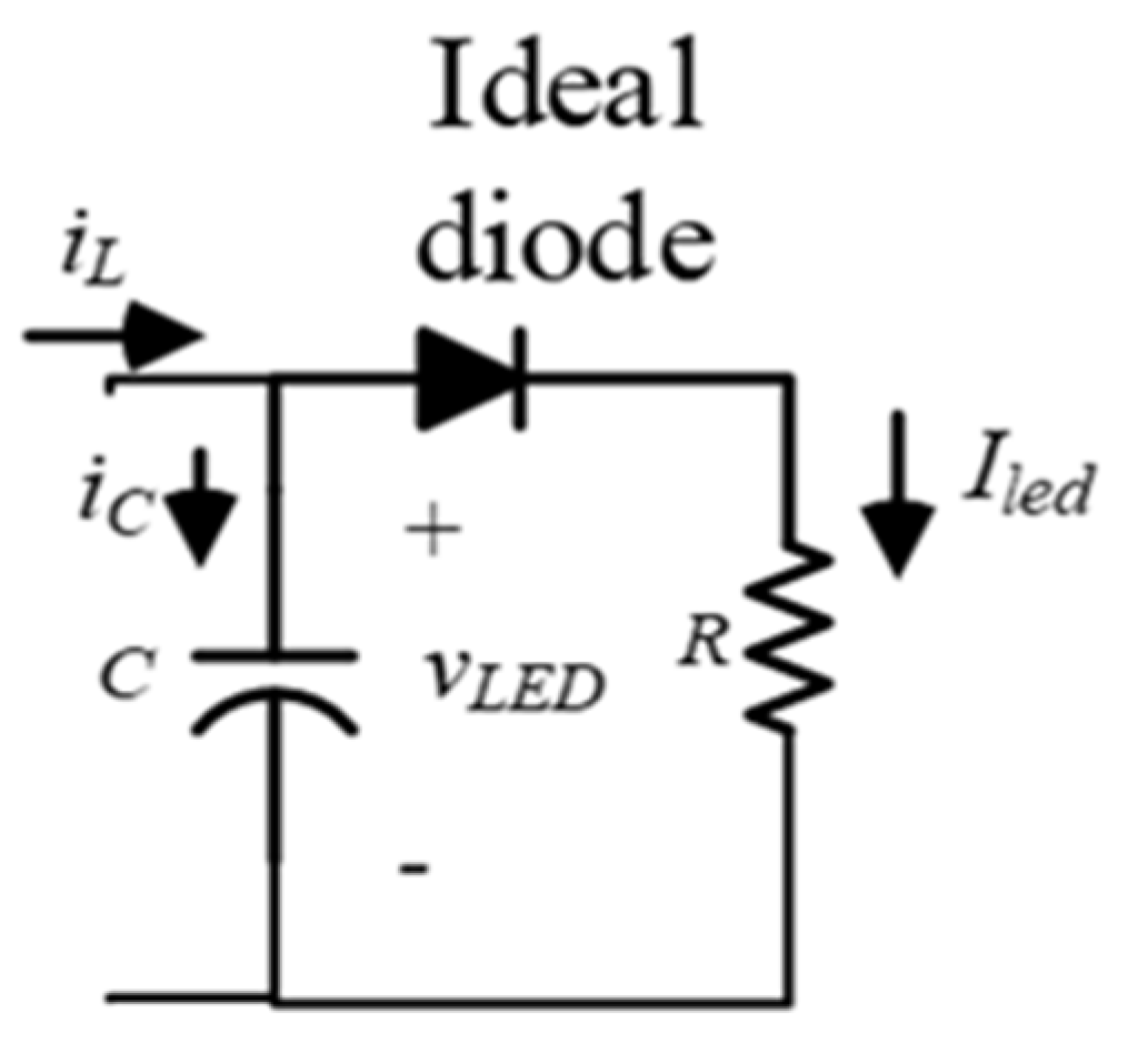
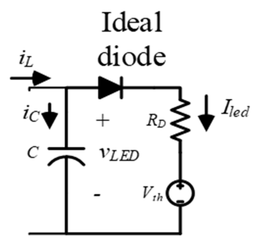
2.1. Model of a Load LED

The physical model of the LED is the well-known Shockley equation. However, this physical model is not very suitable for the design of power converters. A more simplified model involves modeling the converter load as a voltage and resistance source circuit to represent the LED load [12,13]. This paper focused on the operation of the DC-DC buck converter by modeling the LED as a serial voltage source with a resistor. With this analysis, equations are obtained that consider the voltage and current ripples that will influence the output capacitor. The proposed analysis for the output filter of the buck converter is based on the Fourier series and phasors to calculate the elements. The proposed solution guarantees accuracy in the calculation of design elements that are considered fundamental for any LED driver used in lighting systems. The present study aims to evaluate the impact of implementing the Source Voltage Resistor Model (SVRM) to model the LED load, specifically in terms of changes in current and voltage ripples. The SVRM model is composed of an ideal diode in series with a combination of a voltage source that represents the threshold voltage of the LED (VTH) and its characteristic resistance (RLED) represented in Figure 1.
Within the literature, there are models available that replicate the behavior of LEDs, which take into consideration the impact of thermal effects. Such models have been documented in publications such as [10,12]. However, in applications for LED lighting systems, most of the proposed models model the output load (LED lamp) as a resistor, without considering the percentage error implied by this model, because the calculations are based solely on power and voltage, ignoring the actual current circulating in the circuit. As a result, the output waves observed in the circuit do not match those calculated by the modeling.

2.2. LED Linear Modeling

Similar to a conventional diode, the flow of current through an LED commences only when the threshold voltage (Vth) is surpassed. Subsequently, the current increases proportionally to the slope dictated by the characteristic resistance (RLED). The characterization of the load is performed in this case by a strip of LED.
Figure 2 shows the behavior obtained from experimental data for a strip of 300 white LEDs of the brand Concept Car model 3528. The threshold voltage of the LED leads to a shift in its output voltage, consequently changing the correlation between the waveforms of current and voltage. As reported in the literature [14], the voltage of an LED is calculated using the Shockley equation, which is illustrated in Equation (1).
v o = i o R s + E g q + n k T j q ln ( i o C )
where vo is the LED voltage, Rs is the small signal resistance of the LED, io is the LED current, k is the Boltzmann’s constant, Eg is the bandgap energy, Tj is the junction temperature, n is the ideality factor, C is a device parameter and q is the magnitude of the electronic charge. Based on the diode equation, it is evident that the connection between voltage (vo) and current (io) is nonlinear. Nonetheless, Equation (1) is considerably more intricate compared to the SVRM, which serves as a linear approximation.
v o = i o R L E D + V t h
Equation (2) is simpler since it solely reflects the linear slope of the LED’s constant behavior. The non-linear characteristics are incorporated through the use of an ideal SVRM diode, which restricts the flow of current in the opposite direction. The voltage threshold does not operate as a source, and current can only pass through once the voltage surpasses the threshold.

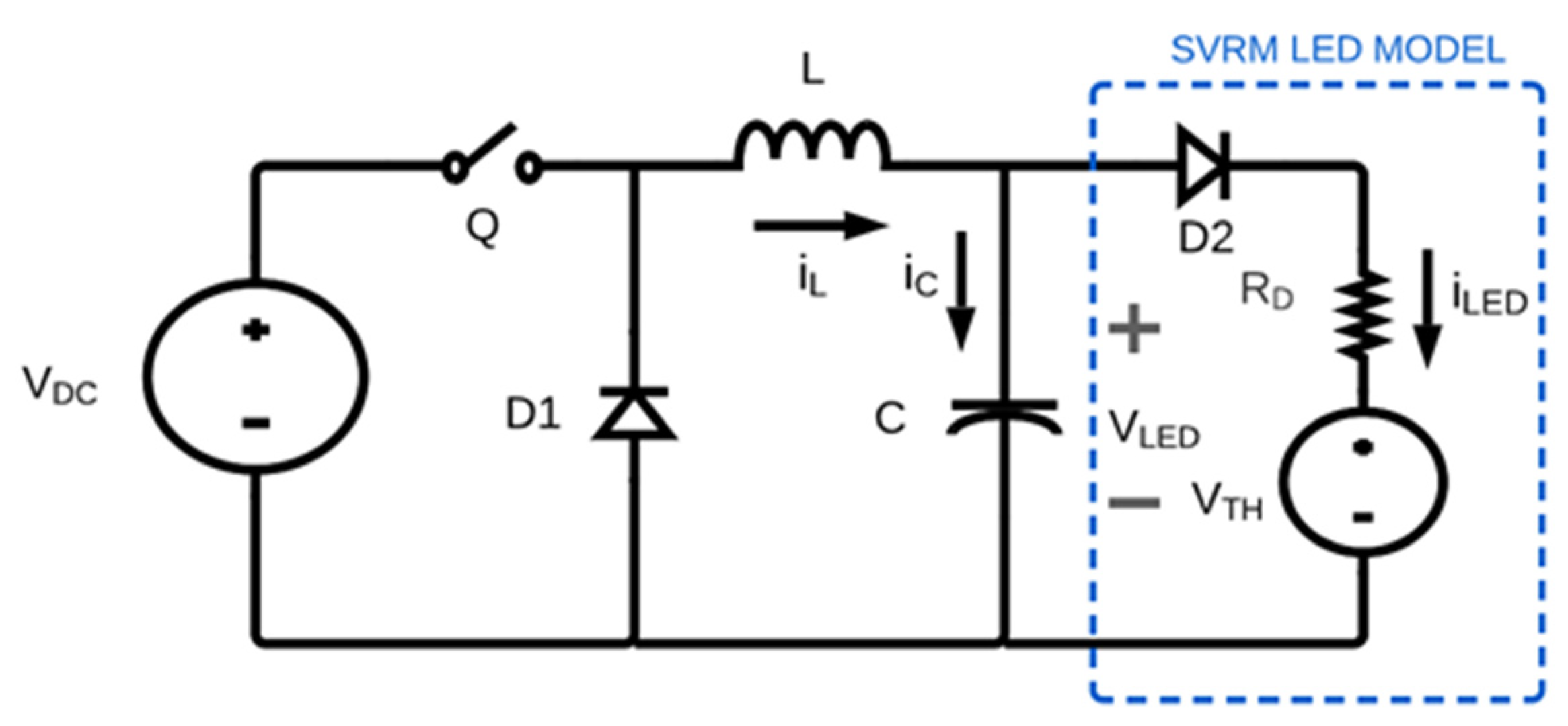
2.3. Analysis of the Equation for Buck Converter with LED Load

The use of the SVRM model of LEDs has been examined and discussed in prior studies [15,16,17]. This section elaborates on the analysis conducted to simulate the performance of the proposed DC-DC buck converter as an LED driver and demonstrates the variances that emerge when the SVRM is treated as a load. It should be noted that the inclusion of the SVRM model parameters will have an impact on the complete analysis of the converter.
The analyzed circuit, consisting of a buck converter, is shown below in Figure 3. To calculate the parameters considering the SVRM model of the circuit, the average current in the LED is obtained by clearing Equation (3).
P = 1 T 0 T i l e d v l e d d t = I l e d V l e d
where Iled and Vled are the average values of iled and vled, respectively. Clearing and substituting the current is obtained as a function of the power, as shown in Equation (4):
I l e d = P V l e d
Subsequently, it is possible to calculate the value of the LED resistance from Ohm’s law:
R D = V l e d V t h I l e d
The duty cycle at which the converter will be operating is determined by Equation (6).
D = V l e d V D C

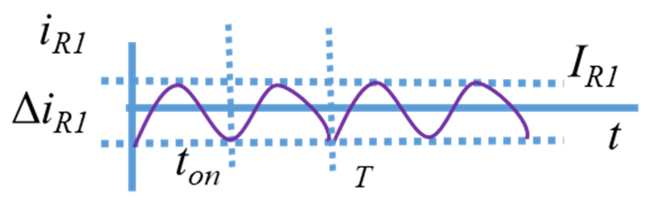
2.3.1. Inductor Equation Analysis

The waveform of the current in the inductor L is assumed for a complete cycle, as shown in Figure 4. In this Figure, Iled represents the average value of the current iL and ΔiL is the ripple.
Analyzing the waveform in the inductor, the equation that defines this graph is:
v L = L d i d t = v D 1 v l e d
And
v D 1 = { V D C 0 < t < t o n 0 t o n < t < T
Taking Figure 4 as a reference, if the switch (Q) is on VD1 = VDC, assuming vled = Vled and equal to its average value:
V D C V l e d = L Δ i L t o n
The “on” time ton from the definition of the duty cycle D can be expressed as:
D = t o n T t o n = D T
Substituting these expressions, it is possible to determine an equation for the value L of the inductor, as developed in the following equation:
L = ( V D C V l e d ) t o n Δ i L = ( V D C V l e d ) D T Δ i L
L = ( V D C V l e d ) D Δ i L f s
Defining the current ripple in the normalized inductor:
r i L = Δ i L I l e d Δ i L = I l e d r i L
where ΔiL is the current ripple in the inductor and Iled is the average current in the LED.

2.3.2. Capacitor Equation Analysis

To determine the value of the output capacitor C, the circuit shown in Figure 5 is analyzed, where iL1 represents the fundamental component of the current in the inductor iL. This circuit can be analyzed using phasors and Fourier series. Since all the harmonics of the current in the inductor are filtered, only the fundamental component and the DC component pass.
I L = I C + I l e d I C = 0 I L = I l e d
where iL1 is the fundamental component of the current in the inductor, iR1 is the fundamental current component in the LED, iC1 is the fundamental component of the current in the capacitor, vC would represent the voltage ripple in the capacitor. Solving by phasors we have a current divider:
I R 1 I L 1 = | j X c R D j X c | I R 1 I L 1 = 1 a = X c R D 2 + X c 2
In Equation (15), Xc represents the reactance of capacitor C for the fundamental frequency, IR1 represents the peak value of the fundamental component of the current in RD, IL1 is the peak value of the fundamental component of the current in the inductor L1 and a is that both IR1 will be reduced concerning IL1. The higher the value of a, the lower the ripple of voltage and current in the load. Clearing C from the above Equation (16) develops the following Equation (17):
1 a = X C R D 2 + X C 2 = 1 ω C R D 2 + 1 ω 2 C 2 = 1 ω 2 C 2 R D 2 + 1 ω 2 C 2 R D 2 = a 2 + 1
C = a 2 + 1 ω R D = a 2 + 1 2 π f s R D
If a >> 1:
C a 2 π f s R D

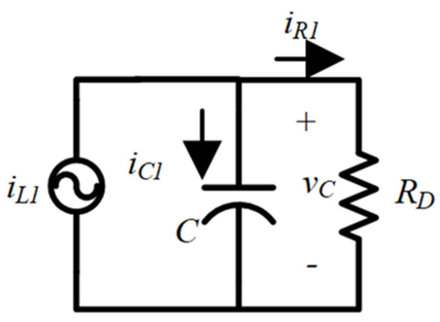
2.3.3. Relationship between Voltage and Current Ripples in the LED

Taking Figure 4 and Figure 5 as a reference, Equation (19) is established:
i L 1 = I L 1 sin ( ω t + ϕ ) = I L 1 sin ( 2 π f s t + ϕ )
where IL1 is the maximum current of iL1. Defining the current ripple in the inductor as the peak-to-peak current of de iL1 yields:
Δ i L I L 1 p p 2 I L 1
Clearing:
Δ i L = r i L I L = r i L I l e d = 2 I L 1
Substituting Equations (20) and (21) establishes:
I L 1 = r i L I l e d 2
Figure 6 shows the fundamental current in the LED iR1. The value IR1 is the maximum value and ΔiR1 is the peak to peak value of the waveform. From the waveform observed in the following Figure 6, and analyzing the circuit of Figure 5, Equation (23) is obtained.
v C 1 = i R 1 R D = V C 1 sin ( ω t ) = V C 1 sin ( 2 π f s t )
where VC1 is the maximum voltage of vC1. Defining the voltage ripple in the capacitor as the peak-to-peak voltage of vC1:
i L 1 = I L 1 sin ( ω t + ϕ ) = I L 1 sin ( 2 π f s t + ϕ )
where IL1 is the maximum current of iL1. Defining the current ripple in the inductor as the peak-to-peak current of iL1 develops:
Δ v c V C 1 p p = 2 V C 1
r v = Δ v C V l e d = 2 V C 1 V l e d = 2 I R 1 R D V l e d
I R 1 = r v V l e d 2 R D
Calculating the converter capacitor based on the voltage and current ripples yields:
I R 1 I L 1 = 1 a = X c R 2 + X c 2 = r v V l e d 2 R D r i L I l e d 2 = r v V l e d r i L I l e d R D
where:
a = r i L I l e d R D r v V l e d

2.3.4. Component Selection from Conduction Losses

To carry out simulations of the proposed topology, it is sought to select a component that adjusts from the conduction losses as a percentage of the total power.
P c M = % P M P
Driving losses can be expressed as:
P c M = I M R M S 2 R d s ( o n )
where Rds(on) is the drainage-source resistance of the component during the power state:
R d s ( o n ) = P c M I M R M S 2 = % P M P I M R M S 2
The effective current is set as:
I M R M S = 1 T 0 T i M 2 d t = 1 T 0 t o n I L 2 d t = I L D = P D 2 V D C
If the losses are proposed as a percentage of the total power, it is possible to select the appropriate one for the converter. This is represented by Equation (34).
R d s ( o n ) = % P M P P 2 D V D C 2 % P M V D C 2 P D

3. Results

This section presents the results obtained from the equations proposed in the previous section. Specifically, a design for a buck converter is proposed using these equations for study purposes. It is notable to observe that the design with these equations considers the parameters of the behavior of the converter circuit with the AC and DC components that intervene in the operation of the source.

3.1. Design Specifications

The equations derived can be utilized to determine the necessary parameters for designing a converter intended for LED lamp applications. The necessary values of the components for the design of the buck converter can be determined. This converter will be connected to a load of LED strips, with the required operation specifications being shown in Table 1.

3.2. Equations for the Buck Converter

Once the operating characteristics of the converter and the required output characteristics are known, Table 2 presents the equations required to determine the necessary component values for designing the buck converter.
For this case, we can observe in the equations of Table 2 that the values of the LED load intervene in the determination of the values required for the design of the converter. These equations not only consider the conditions that would be observed in a solely resistive load, but use the model that allows the parameterizing of the real conditions of the LED load, which allows the more accurate adjustment of the value of the components which are used when manufacturing the converter.

Relationship between Current Ripple and Voltage in the LED

To compare the ripples of current and voltage of the SVRM with the conventional resistive model of the LED. The analysis of the ripples with the resistive model was done. The resistive model of the LED is shown in Figure 7.
Figure 7 model the LED as a resistance R, where iL is the inductor current, iC is the capacitor current and Iled is the current in the resistive model of the LED R.
As can be seen in the figure, from the circuit we can obtain the equations:
r v = r i l e d
Substituting the value in Equation (35) we obtain:
r v = Δ v C V l e d = 2 V C 1 V l e d = 2 I R 1 R D V l e d r i l e d = 2 I R 1 I l e d
And the equation for the voltage in the LED is determined by Equation (38):
r v = Δ v C V l e d = 2 V C 1 V l e d = 2 I R 1 R D V l e d
r i l e d = 2 I R 1 I l e d
The topology for the circuit with SVRM model is shown in Figure 8. In this Figure, RD and Vth represent the SVRM model of the LED.
It was determined by analyzing the equations that describe the circuit that is observed in Figure 8.
r v r i l e d
From Equation (39) is obtained (40):
r v r i l e d = 2 I R 1 R D V l e d 2 I R 1 I l e d = I l e d R D V l e d = I l e d R D V t h + I l e d R D = 1 1 + V t h I l e d R D
when comparing Equations (36) and (40), we can see that there are different parameters involved that define these expressions, which shows that making use of the SVRM model for the LED load allows us to obtain different values than those that would be obtained using the traditional resistive model. The relevance of considering most of the variables that operate in a real way when designing the converter for the LED lamp is to be able to select the appropriate components that extend the useful life of the power supplies, considering the actual margin of error that will apply in the converter.
The equations for the LED model and the SVRM model, are shown in Table 3, where the equations required for each model are compared.
The design parameters for which the converter for the SVRM model is specified are in Table 1, and the parameters for the resistive LED model were the same, except the ripple of current, for in this case the ripple of voltage and current are the same of ri = 0.01
In the following Table 4, a comparison is shown between the voltage and current ripples obtained when using the resistive model and the SVRM model.

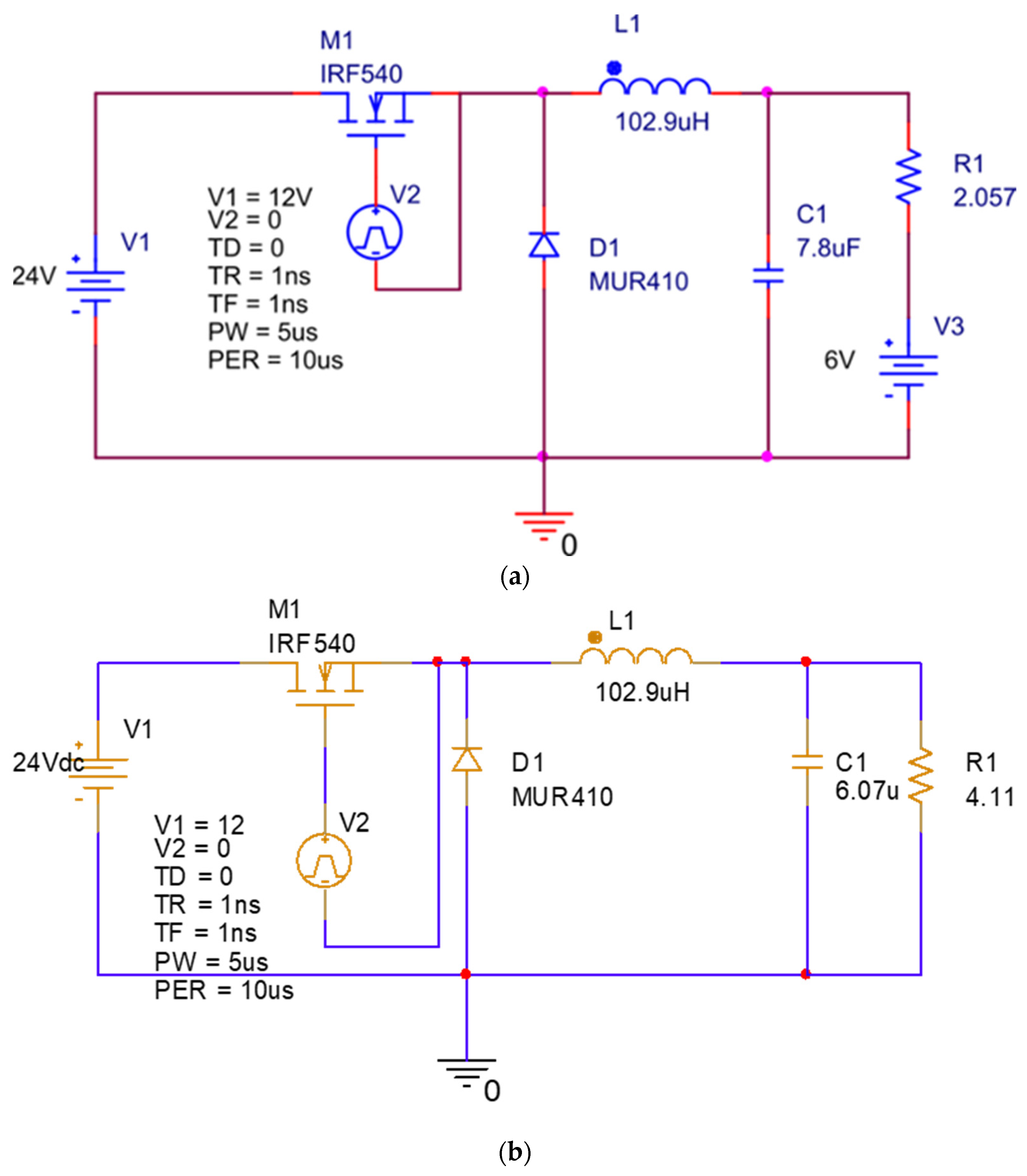
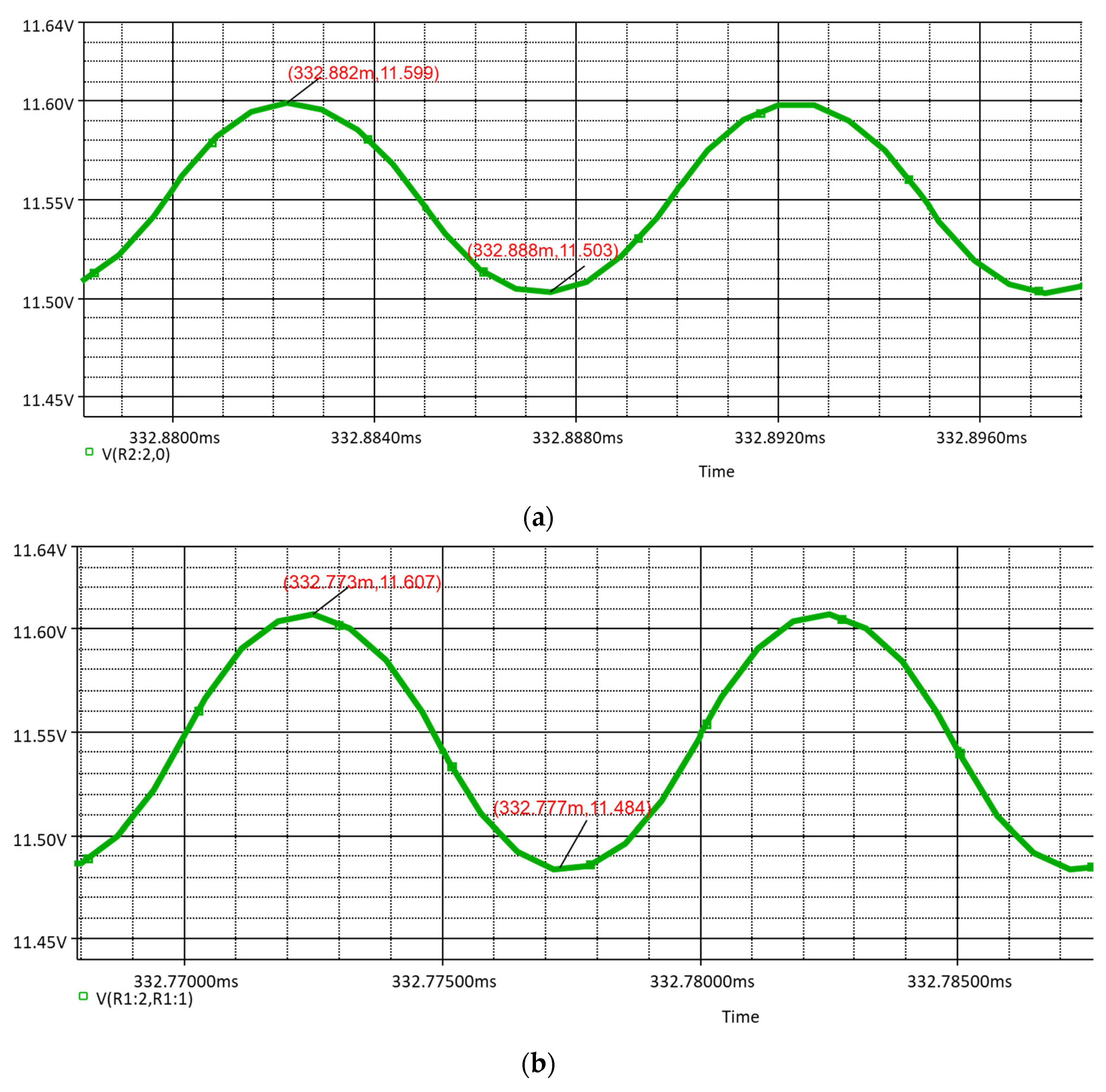
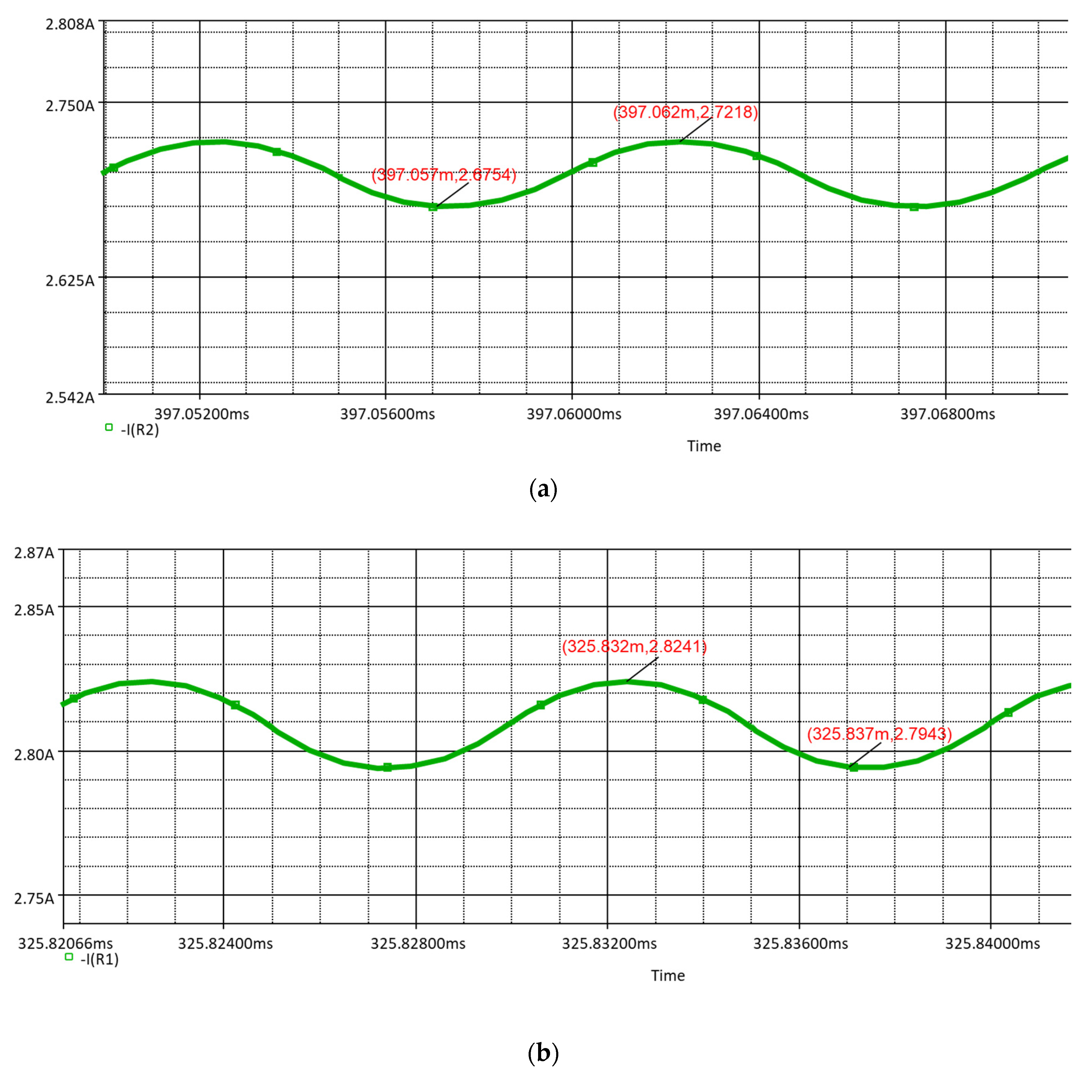
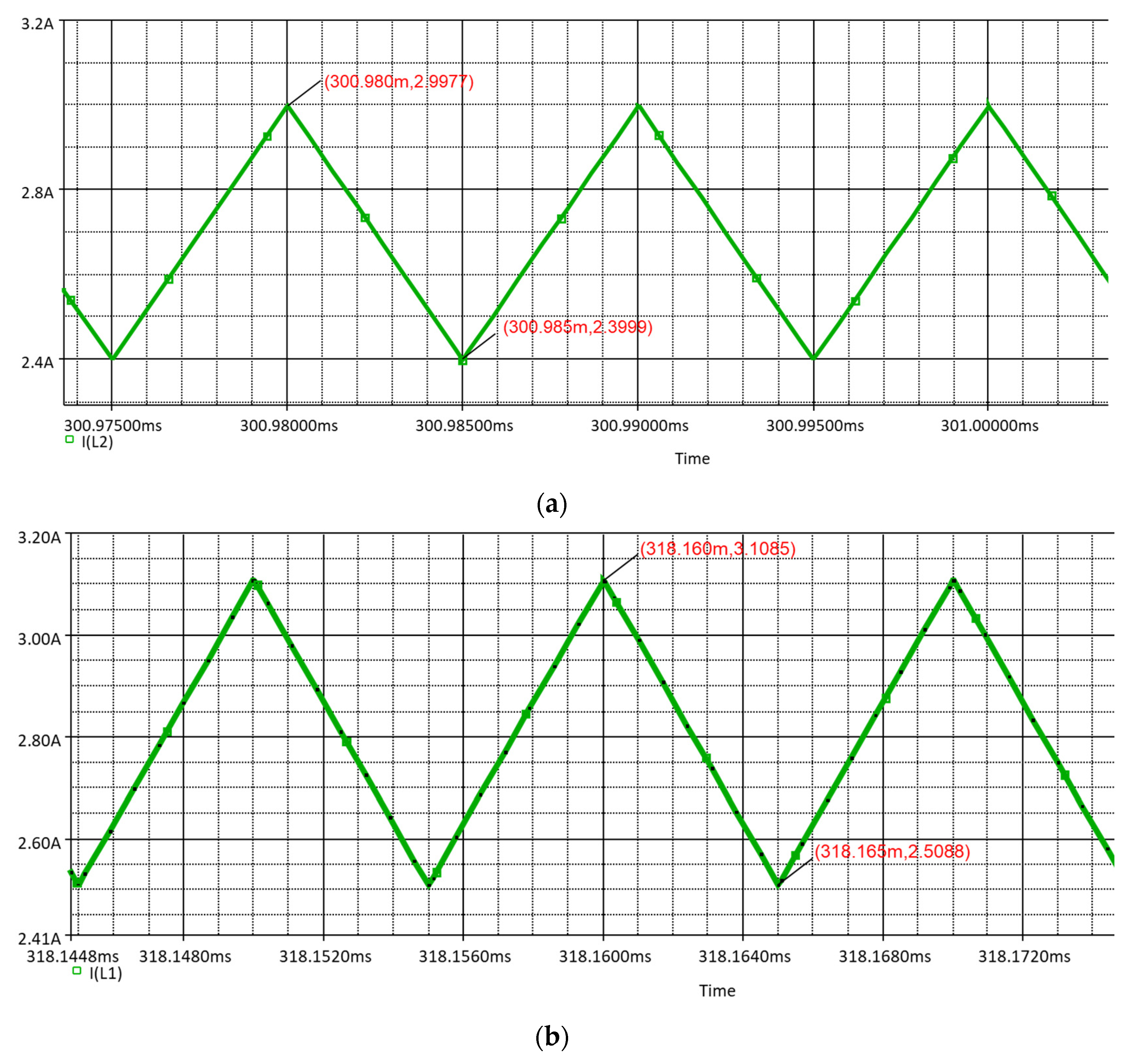
3.3. Circuit Analysis in PSPICE

This paper evaluates the impact of the SVRM in the design of converter LED drivers. The study concludes that the LED load can be represented as a current source with two components, and by analyzing the output circuit (including the capacitor and load) through superposition, an accurate expression to calculate the output capacitor based on the current and voltage ripple percentages can be obtained. The equation used to evaluate the output capacitor for the SVRM was validated through PSPICE simulations.
The behavior analysis of a resistive LED model and an SVRM LED model was conducted through the development of a circuit for an LED driver utilizing a buck converter, illustrated in Figure 9, and implemented in PSPICE. For the purpose of comparison, the buck circuit was simulated with the resistive model Figure 9a and the SVRM model with Figure 9b.
By simulating the buck converter circuit with both the SVRM LED model and the resistive LED model as loads, it is possible to measure the current and voltage in the LED, as well as the current in the inductor. This allows for the verification of the desired ripple values and voltage and current levels across the LED.
Figure 10 shows the voltage graph at the output of the converter for both cases. Figure 10a shows the output votage for the SVRM model and Figure 10b shows the output voltage for resistive model. It is observed that it has an average level of approximately 11.55 V. It is also appreciated that it has a maximum level of 11.59 V and a minimum value of 11.503 V, which gives a ripple of 0.096 V. This is close to the desired value (0.01 normalized, which is equivalent to 0.12 V).
On the other hand, in Figure 11 the graphs obtained by measuring the output current in the converter load for both cases are shown. Figure 11a shows the output current of the SVRM model and, Figure 11b shows the output current for the resistive LED model. It can be observed in graph (a) that for the SVRM model, there is an average current of 2.71 A. It has a maximum peak value of 2.722 A and a minimum value of 2.675 A, which results in a ripple of riLED = 0.018. On the other hand, for the resistive LED model the current ripple is ri = 0.010.
In Figure 12, the graphs corresponding to measuring the current flowing through the inductor for the resistor LED model and the SVRM LED model are shown. We can observe in Figure 12a that there is a maximum peak value of 2.998 A, and a minimum value of 2.3985 A, which results in a current ripple in the inductor of 0.5995 A, which is too close to the required value (0.2 normalized, which is equal to 0.583 A).
The following Table 5 shows the data obtained for each variable mentioned, both in simulation tests and the methodology presented in this document, as well as the percentage of error between both values obtained.
In Table 5 presented, we can analyze that the error percentages obtained are small, which helps to determine that it is possible to implement the design of this converter using these equations to calculate the components of the power supply for the LED lamp.
The simulation of a buck converter with an LED as a load was presented. For this simulation and the design of the converter, the SVRM model of the LED was considered, which contemplates a resistance in series with a voltage source. This model is too close to the actual operating characteristics in the components, and in many cases is more than sufficient for the development of LED lamp power systems, as well as their possible controllers. With the development of this work, a method is proposed that allows us to analyze in greater detail the design of a buck converter, mainly in the output filter, managing to improve the precision in the values of the elements involved in the topology of the converter. If the current in the LED is very small, the difference between ripples will be greater, and analogously, the higher the current in the LED, the greater the difference between ripples. On the other hand, it can be observed that the average voltage and average current levels at the output vary from the specifications. This is mainly due to the losses that occur in both the interrupter and the diode. To compensate for these losses, it may be enough to increase the duty cycle.

4. Discussion

This work presents an equation for the most accurate output capacitor for the value of the elements for the design of the buck circuit. The analysis of the RC filter is based on the Fourier series and a phasor analysis so the development proposed in the previous document applies to any DC-DC converter with an RC filter at the output and current source feeding the filter. It is demonstrated that, based on the V-I behavior of LEDs, the current and voltage ripples in the LED will always be different, with the current ripple always being greater than the voltage ripple.
In this study, the impact of SVRM on the design of LED lamp drivers has been examined. The analysis presented in the paper shows that the output of a buck converter, when driving an LED load, can be modeled as a current source with two components: a DC component and an AC component with a frequency that is twice the line frequency. By using superposition, it is possible to derive an equation that accurately calculates the required output capacitance based on the desired current and voltage ripple percentages. The equation used to evaluate the output capacitor for the SVRM was compared using SPICE simulations, obtaining an error of less than 3%. The analysis conducted in this study also demonstrated that the current ripple percentage is invariably higher than the voltage ripple percentage in the presence of an LED load (%RvLED < %RiLED). The dissimilarities between the models primarily pertain to the capacitance of the circuit, stored energy and voltage ripple percentage wherein the SVRM stores significantly more energy owing to the use of a larger capacitor, while the voltage ripple percentage remains minute owing to the voltage threshold.

Author Contributions

Conceptualization, M.P.-S. and R.C.A.-M.; formal analysis, M.P.-S.; methodology, M.P.-S., R.C.A.-M. and G.S.O.-C., software, R.C.A.-M. and G.S.O.-C.; validation, M.P.-S.; investigation, R.C.A.-M. and G.S.O.-C.; resources, M.P.-S. and R.C.A.-M..; writing—original draft preparation, M.P.-S. and R.C.A.-M.; writing—review and editing, R.C.A.-M. and G.S.O.-C.; visualization, G.S.O.-C.; supervision, M.P.-S.; project administration, M.P.-S. All authors have read and agreed to the published version of the manuscript.

Funding

This research received no external funding.

Informed Consent Statement

Not applicable.

Conflicts of Interest

The authors declare no conflict of interest.

References

  1. Wang, S.; Ruan, X.; Yao, K.; Tan, S.C.; Yang, Y.; Ye, Z. A Flicker-Free Electrolytic Capacitor-Less AC–DC LED Driver. IEEE Trans. Power Electron. 2012, 27, 4540–4548. [Google Scholar] [CrossRef]
  2. Alonso, J.M.; Vina, J.; Vaquero, D.G.; Martinez, G.; Osorio, R. Analysis and Design of the Integrated Double Buck–Boost Converter as a High-Power-Factor Driver for Power-LED Lamps. IEEE Trans. Ind. Electron. 2012, 59, 1689–1697. [Google Scholar] [CrossRef]
  3. Pai, N.; Kini, S.G. Design and Prototyping of Dimmable LED Driver for General Lighting Application. In Proceedings of the 2018 Second International Conference on Electronics, Communication and Aerospace Technology (ICECA), Coimbatore, India, 29–31 March 2018; pp. 1–6. [Google Scholar]
  4. Agrawal, A.; Jana, K.C.; Shrivastava, A. A review of different DC/DC converters for power quality improvement in LED lighting load. In Proceedings of the 2015 International Conference on Energy Economics and Environment (ICEEE), Greater Noida, India, 27–28 March 2015; pp. 1–6. [Google Scholar]
  5. Wang, Y.; Alonso, J.M.; Ruan, X. A Review of LED Drivers and Related Technologies. IEEE Trans. Ind. Electron. 2017, 64, 5754–5765. [Google Scholar] [CrossRef]
  6. Mrabet, B.M.; Chammam, A.; Nsibi, W. Constant-Current LEDs driver based on DC-DC buck converter with dimming capability. In Proceedings of the 2020 6th IEEE International Energy Conference (ENERGYCon), Gammarth, Tunisia, 28 September–1 October 2020; pp. 204–209. [Google Scholar]
  7. Papenfuss, F.; Timmermann, D. Alias-Free Periodic Signal Analysis using Efficient Rate Nonuniform Sampling Sets. In Proceedings of the 2007 IEEE International Conference on Acoustics, Speech and Signal Processing—ICASSP ‘07, Honolulu, HI, USA, 15–20 April 2007; Volume 3, pp. III-1497–III-1500. [Google Scholar]
  8. Saad, H.; Peralta, J.; Dennetière, S.; Mahseredjian, J.; Jatskevich, J.; Martinez, J.A.; Davoudi, A.; Saeedifard, M.; Sood, V.; Wang, X.; et al. Dynamic Averaged and Simplified Models for MMC-Based HVDC Transmission Systems. IEEE Trans. Power Deliv. 2013, 28, 1723–1730. [Google Scholar] [CrossRef]
  9. Cheng, C.-A.; Chang, C.-H.; Cheng, H.-L.; Chang, E.-C.; Chung, T.-Y.; Chang, M.-T. A Single-Stage LED Streetlight Driver with Soft-Switching and Interleaved PFC Features. Electronics 2019, 8, 911. [Google Scholar] [CrossRef]
  10. Abdelmlek, K.B.; Araoud, Z.; Canale, L.; Nejma, F.B.; Charrada, K.; Zissis, G. Thermal management of LEDs packages within inclined enclosures for lighting applications. In Proceedings of the 2021 IEEE Industry Applications Society Annual Meeting (IAS), Vancouver, BC, Canada, 10–14 October 2021; pp. 1–6. [Google Scholar]
  11. Salazar-Pérez, D.; Ponce-Silva, M.; Aqui, J.; García-Guzmán, J.; Pérez-Cruz, J. Effects of the LED modelling on the output capacitance of power converters. IET Power Electron. 2020, 13, 3467–3474. [Google Scholar] [CrossRef]
  12. Górecki, K.; Ptak, P. Modelling LED lamps in SPICE with thermal phenomena taken into account. Microelectron. Reliab. 2017, 79, 440–447. [Google Scholar] [CrossRef]
  13. Salazar-Pérez, D.; Ponce-Silva, M.; Alonso, J.M.; Aquí-Tapia, J.A.; Cortés-García, C. A Novel High-Power-Factor Electrolytic-Capacitorless LED Driver Based on Ripple Port. IEEE J. Emerg. Sel. Top. Power Electron. 2021, 9, 6248–6258. [Google Scholar] [CrossRef]
  14. Shockley, W. The theory of p-n junctions in semiconductors and p-n junction transistors. Bell Syst. Tech. J. 1949, 28, 435–489. [Google Scholar] [CrossRef]
  15. Lam, J.C.W.; Jain, P.K. A High Power Factor, Electrolytic Capacitor-Less AC-Input LED Driver Topology With High Frequency Pulsating Output Current. IEEE Trans. Power Electron. 2015, 30, 943–955. [Google Scholar] [CrossRef]
  16. Wang, B.; Ruan, X.; Yao, K.; Xu, M. A Method of Reducing the Peak-to-Average Ratio of LED Current for Electrolytic Capacitor-Less AC–DC Drivers. IEEE Trans. Power Electron. 2010, 25, 592–601. [Google Scholar] [CrossRef]
  17. Yan, L.; Chen, B. New developments in dimmable LED driver controllers. In Proceedings of the 2014 11th China International Forum on Solid State Lighting (SSLCHINA), Guangzhou, China, 6–8 November 2014; pp. 92–96. [Google Scholar]
  18. Ang, S.; Oliva, A. Power-Switching Converters, 3rd ed.; CRC Press: Boca Raton, FL, USA, 2010. [Google Scholar]
Figure 1. Resistive and SVRM LED model.
Eng 04 00080 g001
Figure 2. V-I curve of the LED strip model 3528.
Eng 04 00080 g002
Figure 3. Buck converter circuit with SVRM model.
Eng 04 00080 g003
Figure 4. Inductor current waveform.
Eng 04 00080 g004
Figure 5. Circuit analysis for capacitor calculation.
Eng 04 00080 g005
Figure 6. Fundamental component of the current waveform in the LED.
Eng 04 00080 g006
Figure 7. Resistive LED model.
Eng 04 00080 g007
Figure 8. SVRM LED model.
Eng 04 00080 g008
Figure 9. Buck converter simulated in PSPICE (a) Resistive LED model (b) SVRM LED model.
Eng 04 00080 g009
Figure 10. Buck converter output voltage graph (a) SVRM LED model (b) Resistive LED model.
Eng 04 00080 g010
Figure 11. Buck converter output current graph. (a) SVRM LED model (b) Resistive LED model.
Eng 04 00080 g011
Figure 12. Graph of the current in the inductor of the buck converter. (a) SVRM LED model (b) Resistive LED model.
Eng 04 00080 g012
Table 1. Parameter specifications of the buck converter.
ParameterSymbolValue
Voltage on the LEDVLED12 V
Threshold VoltageVth9.1 V
LED ResistanceRD7.76 Ω
PowerP5.84 W
Switching frequency f s 100 kHz
Supply voltageVDC24 V
Normalized voltage ripple r v 0.01
Normalized current ripple r i L 0.2
Table 2. Equations for the Buck converter.
ParameterEquationValue
LED Current I l e d = P V l e d 35   W 12   V = 2.916   A
LED Resistance R D = V l e d V t h I l e d 12   V 6   V 2.916   A = 2.057   Ω
Duty Cycle D = V l e d V D C 12   V 24   V = 0.5
Inductor L = ( V D C V l e d ) D I l e d r i L f s ( 24   V 12   V ) 0.5 ( 2.916   A ) ( 0.2 ) ( 10 5   Hz ) = 102.9   μ H
Capacitor C = ( r i L I l e d R D r v V l e d ) 2 + 1 2 π f s R D 7.8   μ F
The losses in transistor R d s ( o n ) % P M V D C 2 P D ( 0.02 ) ( 24   V ) 2 ( 35   W ) 0.5 0.65
Table 3. Comparison between equations for the resistive LED model and SVRM LED model.
ParameterResistive LED Model [18]ValueSVRM ModelValue
Inductor L = ( V i n V o ) D Δ i L f s 102.88   μ H L = ( V D C V l e d ) D I l e d r i L f s 102.9   μ H
Capacitor C = V o ( 1 D ) 8 Δ V o L f s 2 6.07   μ F C = ( r i L I l e d R D r v V l e d ) 2 + 1 2 π f s R D 7.8   μ F
Resistor R = V o I o 4.1   Ω R D = V l e d V t h I l e d 2.05   Ω
Table 4. Comparison between current and voltage ripples for LED model and SVRM model.
ParameterResistive LED Model SVRM Model
Output current I o = V o R e q I o = V o V t h R L E D
Ripple voltage r v = 2 V a c V o r v = 2 V a c V o
Ripple current r i = 2 I a c I o r i L E D = 2 I a c I o = 2 V a c V o V t h
Ratio between voltage and current ripple k r = r i r v = 1 k r L E D = r i L E D r v L E D = 1 1 ( V t h / V o )
Table 5. Comparison between results calculations for LED model.
ValueTheoretical SimulationError %
Vavg, V1211.81.66%
IL, mA97.4101.033.69%
% RiL20%20.73%0.73%
% RV LED1%0.8%0.2%
Disclaimer/Publisher’s Note: The statements, opinions and data contained in all publications are solely those of the individual author(s) and contributor(s) and not of MDPI and/or the editor(s). MDPI and/or the editor(s) disclaim responsibility for any injury to people or property resulting from any ideas, methods, instructions or products referred to in the content.

