Review

A Review of Techniques to Enhance an Amplifier’s Performance Using Resistive Local Common Mode Feedback

by
Jaime Ramirez-Angulo
1,*,
Antonio J. Lopez-Martin
2,
Ramón G. Carvajal
3,
Antonio Torralba
3 and
Jesus Huerta-Chua
1
1
Instituto Tecnológico Superior de Poza Rica, Poza Rica 93230, Mexico
2
Institute for Smart Cities, Universidad Publica de Pamplona, 31006 Pamplona, Spain
3
Department of Electronic Engineering, University of Seville, 41092 Sevilla, Spain
*
Author to whom correspondence should be addressed.
Eng 2023, 4(1), 780-798; https://doi.org/10.3390/eng4010047
Submission received: 26 December 2022 / Revised: 7 February 2023 / Accepted: 20 February 2023 / Published: 1 March 2023
(This article belongs to the Section Electrical and Electronic Engineering)

Abstract

:
A review of some of the most common applications of the resistive local common mode feedback technique to enhance amplifier’s performance is presented. It is shown that this simple technique offers essential improvement in open loop gain, gain-bandwidth product, slew rate, common mode rejection ratio, power supply rejection ratio, etc. This is achieved without increasing power dissipation or supply voltage requirements and with small additional silicon area and circuit complexity. It is also shown that it is especially appropriate to improve amplifiers’ performance in current fine-line submicrometer CMOS technology. Some of the applications discussed are GB enhanced, class AB and super class AB operational amplifiers, gain boosted op-amps, bulk-driven circuits, sample and hold circuits and power management circuits, among others.

1. Introduction

The differential amplifier is used as the input stage of most op-amps. Figure 1a–c show differential pairs loaded with conventional resistive loads, diode-connected and high impedance current source active loads, respectively. For Vi+ = Vid/2 and Vi− = −Vid/2, Vod = Va − Vb the differential voltage gain Ad = Vod/Vid is given by Ad = gm1 RL where RL is the effective load resistance. In Figure 1a RL = R||ro1||ro2 = R′. For Figure 1b RL = [1/(gm2||ro1||ro2)] ≈ 1/gm2 and Ad ≈ [(kn/kp)(W/L)1/(W/L)2]1/2. For Figure 1c the load is RL = ro1||ro2 and the gain Ad ≈ gm1ro/2 ≈ Aint/2, where gm denotes the small signal transconductance gain, ro the output resistance, kn and kp the transconductance parameters of PMOS and NMOS transistors, respectively, and Aint = gmro the intrinsic gain of the MOS transistor. Aint is in the range from 25 to 50 in current fine-line CMOS technology. Increasing R in Figure 1a allows to increase the gain at the expense of a higher quiescent drop VR = IBR caused by the bias current IBIAS in the load resistors R. This drop limits the maximum value of R and also limits the maximum gain that can be achieved from this circuit to values well below the intrinsic gain. In current technologies, this limitation is especially severe due to the sub-volt supply voltages Vsupply < 1V used. The gain of Figure 1b is usually limited to values below 5 since it is proportional to the square root of the ratio (W/L)1/(W/L)2 and large gain values require very large transistor ratios. The gain of the circuit of Figure 1b can be boosted using positive feedback (using transistors M2pf and M2Ppf shown in red). In this case, the gain is given by Ad = gm1/(gm2 − gm2pf). In practice, Ad is kept below 8–10 in order to prevent the circuit to perform as a latch because values of gm2pf very close to gm2 manufacturing tolerances can result in gm2pf > gm2 which causes positive feedback to dominate and the circuit to perform as a latch. The circuit of Figure 1c has a gain of Ad = Aint/2. The cascoded version of Figure 1c (not shown in Figure 1) can offer much higher gain (by a factor of Aint) but it is difficult to use in modern technology since, as indicated above, sub-volt supply voltages prevent utilization of cascode transistors, especially in the output amplifier’s stage. The circuit of Figure 1c requires a control voltage Vx to generate quiescent currents in IM2, IM2P that accurately match the bias currents Ia = Ib = IBIAS in transistors M1, M1P (otherwise nodes a and b would easily go into saturation causing the amplifier to be non-functional). This is only possible if the circuit is part of an op-amp with global negative feedback or if it is used as a standalone amplifier, in which case, an additional, relatively complex, control circuit is required.

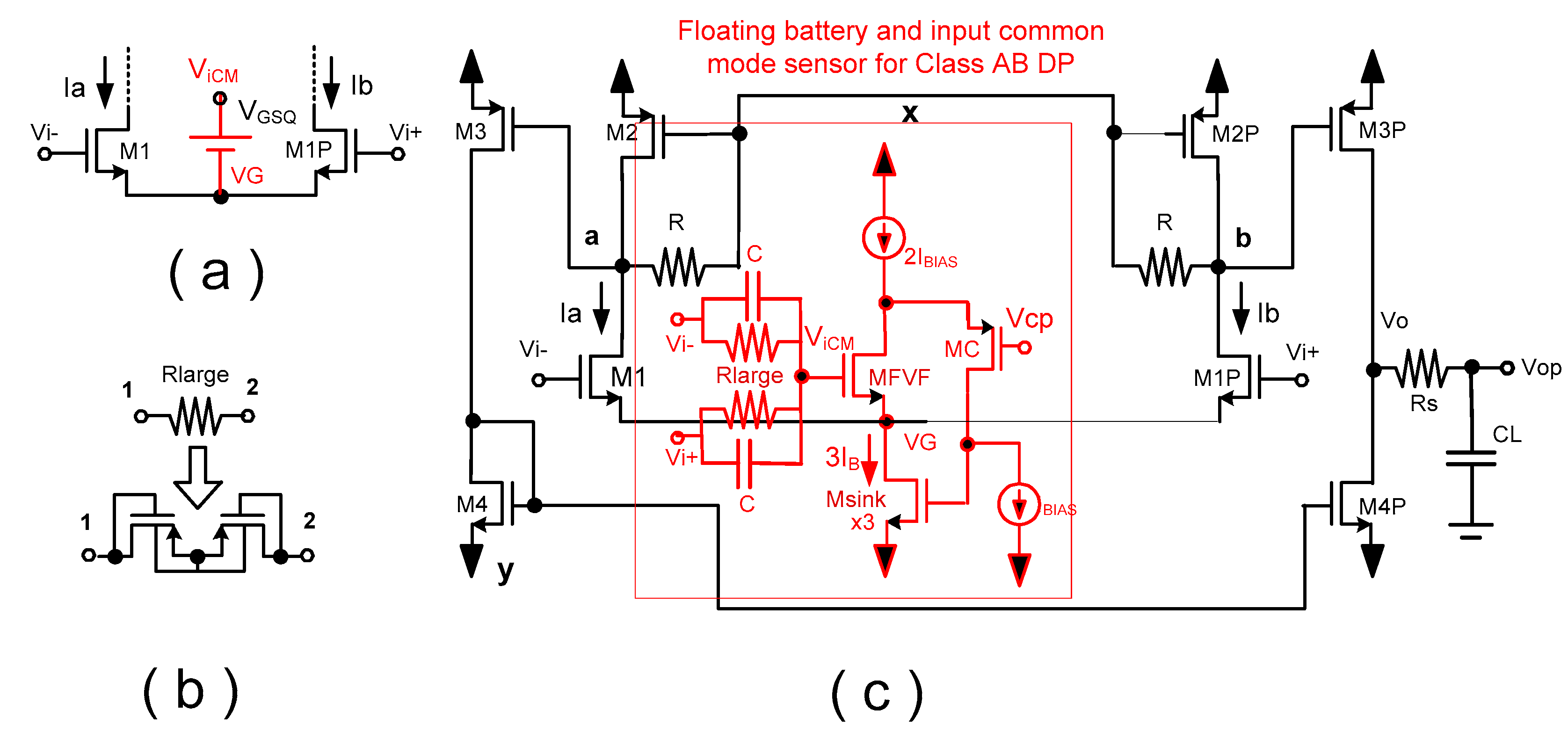
2. Differential Pair with Resistive Local Common Mode Feedback

In this section, we discuss in detail the operation of the differential pair with resistive local common feedback of Figure 1d and compare its performance characteristics with those of the circuit of Figure 1b.

2.1. Operation under Quiescent Conditions (Vi+ = Vi− = 0)

This is illustrated in Figure 2a. Based on symmetry considerations it can be seen that resistors R have zero current (IR = 0). Since no quiescent drop is found across these resistors transistors M2 and M2P behave as diode-connected transistors and the quiescent voltages VaQ, VbQ and VxQ have all equal values VaQ = VbQ = VDD − VSGQ2, where VSGQ2 is the quiescent source-gate voltage of M2, M2P. Transistors M3 and M3P have a quiescent current ID3Q = MIBIAS (assuming (W/L)3 = M(W/L)2). Notice that, as opposed to the circuit of Figure 1a, R can have arbitrarily large values since given that no quiescent current flows through R its value does not affect the value of the quiescent voltages VaQ, VbQ and of the quiescent currents in M3, M3P.

2.2. Differential Operation

The differential operation is illustrated in Figure 2b. Upon application of complementary differential input signals Vi+ = Vid/2, Vi− = −Vid/2 equal but opposite AC signal currents i = gmVid(t)/2 are generated in M1 and M1P so that iA = IBIAS + i, iB = IBIAS − i. The signal currents “i” flow through resistors R generating complementary voltage changes vA = VaQ − iR, vB = VbQ + iR. The currents in M2, M2P, and the voltage Vx remain constant with their quiescent value: IM2 = IM2P = IBIAS, VxQ = VDD − VSGQ2. It can be seen that node x behaves as a signal ground for differential signals. The effective load for differential signals is R′ = R||ro1||ro2. The poles for differential signals at nodes a,b are given by ωpa,b = 1/(R′Ca,b) where Ca,b = Cgd2 + Cgd1 + Cgs3 are the parasitic capacitances at nodes a, b. The maximum value of R′ for R >> ro1, ro2 is given by R′ ≈ ro1||ro2. The gain Ad for differential signals is given by Ad = Vo/Vid = gm1R′ (where Vo = Va − Vb) and its maximum value (for R >> ro1||ro2) is given by Admax = Aint/2. This is similar to the gain of the high impedance active loaded circuit of Figure 1c. In practice, R can be used to set a compromise between the differential gain and the poles ωpa,b at nodes a and b. Notice that CGS2 does not contribute to Ca,b and with the drastic reduction of feature sizes in modern CMOS technologies parasitic capacitances Ca,b are so small (in the 10 s of fF range) that the poles ωpa,b remain at relatively high frequencies (MHz) even for large R′ values for R >> ro1||ro2 in which case ωpa,b = 2/(roCa,b). For large R′ values voltages Va,b are subject to large negative variations ΔVa,bpeak = −ΔIBR′ which lead to large peak currents in M3, M3P, that can be much larger than the bias current IBIAS (approximately by a factor of K = (MIBIASR′/VDSSat)2 where VDssat = VGS − VTH is the drain–source saturation voltage of M3, M3P). This feature allows, besides relatively high gain, improved gain-bandwidth and CMRR, also efficient class AB operation in amplifiers where the circuit of Figure 1d is used. This is shown in the following section.

2.3. Common Mode Operation

This is illustrated in Figure 2c. Upon application of common mode input signals Vi+(t) = Vi−(t) = Vicm(t) and based again on symmetry considerations the currents IR in R have zero value and the currents in M1, M1P acquire a small signal common mode component icm: where icm ≈ Vcm/2rotail. The load resistance for common mode signals is R′cm ≈ 1/gm2; therefore, the voltages at nodes Va, Vb and Vx are all equal and subject to very small variations vacm = vbcm = vXcm = icm(1/gm2). The common mode gain at nodes a,b is then given by Acma,b = va,bcm/vcm = ≈1/(2 gm2rotail). If the output is taken differentially: Vocm = Voacm − Vobcm the common mode gain is given by Acm = Vocm/Vicm ≈ [Δ(1/gm2)/(2rotail)]. Where Δ(1/gm2) = (1/gm2) − (1/gm2P) is the mismatch error in the values of 1/gm2 and 1/gm2P. Typically, using adequate analog layout techniques, mismatch errors Δ(1/gm2) are approximately two orders of magnitude smaller than 1/gm2: Δ(1/gm2) ~ 0.01(1/gm2) ≈ 1/(100gm2) which leads to Acm~1/(200 gm2rotail). The common mode rejection ratio for the circuit of Figure 1d is very high and approximately given by CMRR = Ad/Acm = 100 (gm1R′)(2 gm2rotail). The circuits of Figure 1a–c, have all the same load for common mode and for differential signals, and their common mode rejection ratio is given by CMRR = (gm12rotail)/(ΔR′/R′)~200 gm1rotail or CMRR~200Aint. It can be seen that CMRR is a factor of Kenh = gm1R′ higher for the RLCMFB circuit of Figure 1d than for the circuits of Figure 1a–c. The poles for common mode signals at nodes a, b in the circuit of Figure 1d are high-frequency poles given by ωpcma,b = gm2/Ca,b. In Section 3, it is shown that this same improvement factor Kenh is achieved for GB, the open loop gain Aol and the small and large signal figures of merit of OTAs where the circuit of Figure 1d is used as the input stage.

2.4. Some Remarks on the Operation of the Circuit of Figure 1d

The above discussion can be summarized by stating that in the circuit of Figure 1d, the load and poles for common mode signals and differential signals are very different. For common mode signals the load is low and has a value R′cm = (1/gm2) while the load for differential signals can be high R′ = R||ro1||ro2. For high R values, the differential gain Ad can take values close to the intrinsic gain while common mode signals have close to unity gain much lower than for the circuits of Figure 1a,c. In current CMOS technologies the poles ωpa,b at nodes a, b for differential signals are medium-high frequency poles (~MHz) and for common mode signals the poles at nodes a,b are high-frequency poles. In the circuits of Figure 1a–c the load R′ and the poles ωpa,b for differential and common mode signals are the same ωpa,b=1/(R′Ca,b). For this reason, the CMRR of the circuit of Figure 1d is a factor of Kenh higher than for the circuits of Figure 1a–1c as will be shown in the next section.
Another important point to notice is that since no quiescent current flows in resistors R, their value does not affect the quiescent voltages VaQ, VbQ and it does not limit the peak swing at the output nodes a, b. The quiescent current in the output branch transistors, M3 and M3P, is accurately determined by the quiescent voltages VaQ, VbQ and has a value ID3Q = MIBIAS independent of the value of R. The peak swing in the negative direction of voltages Va and Vb is given by Δva = −2IBR′. This can generate very large peak currents IM3PK (much higher than the bias current IBIAS) in transistors M3 and M3P driven by Va and Vb. In order to save silicon area, as discussed in [1], resistors R can be implemented with transistors in triode mode which has the advantage of making them programmable.

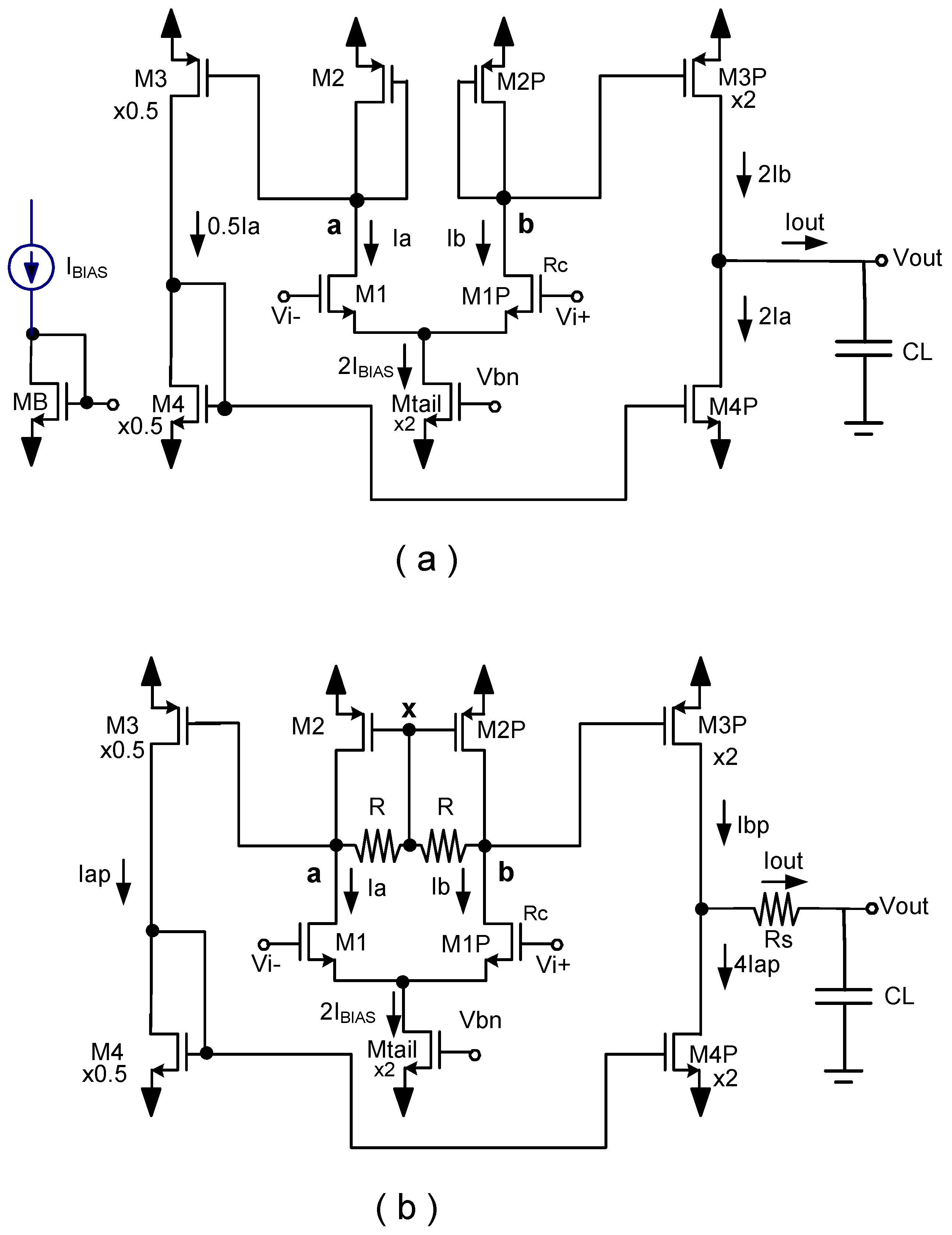
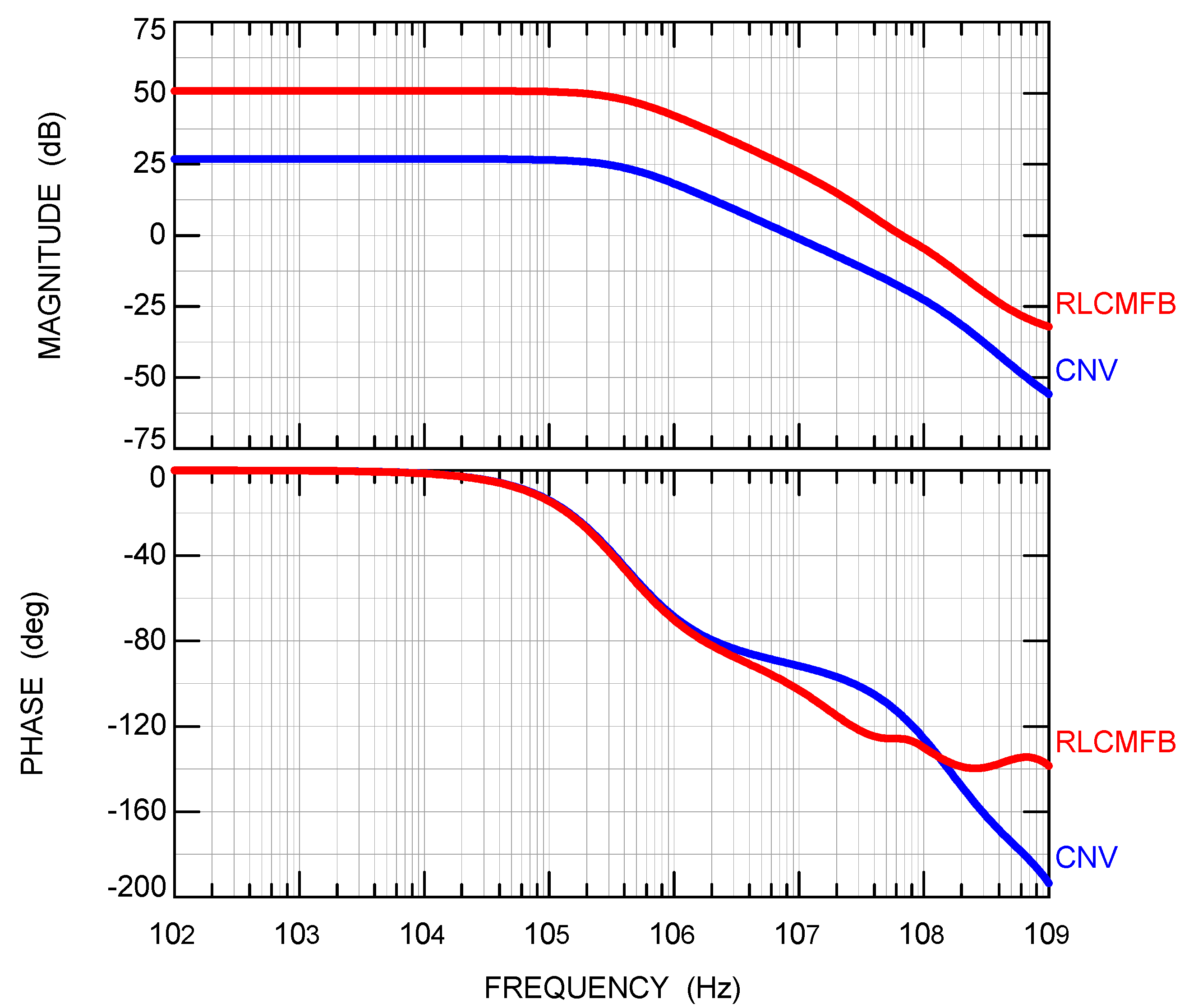
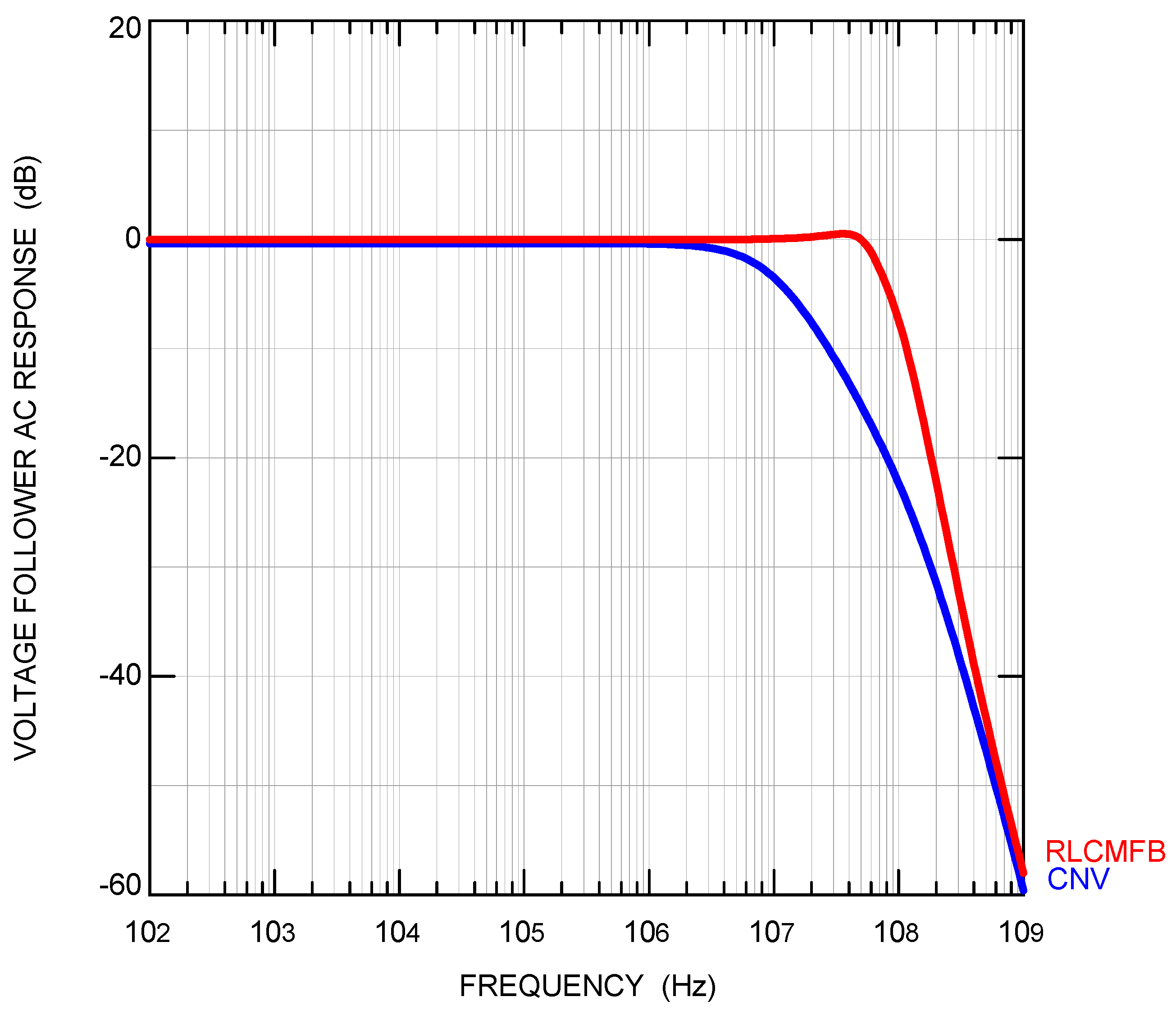
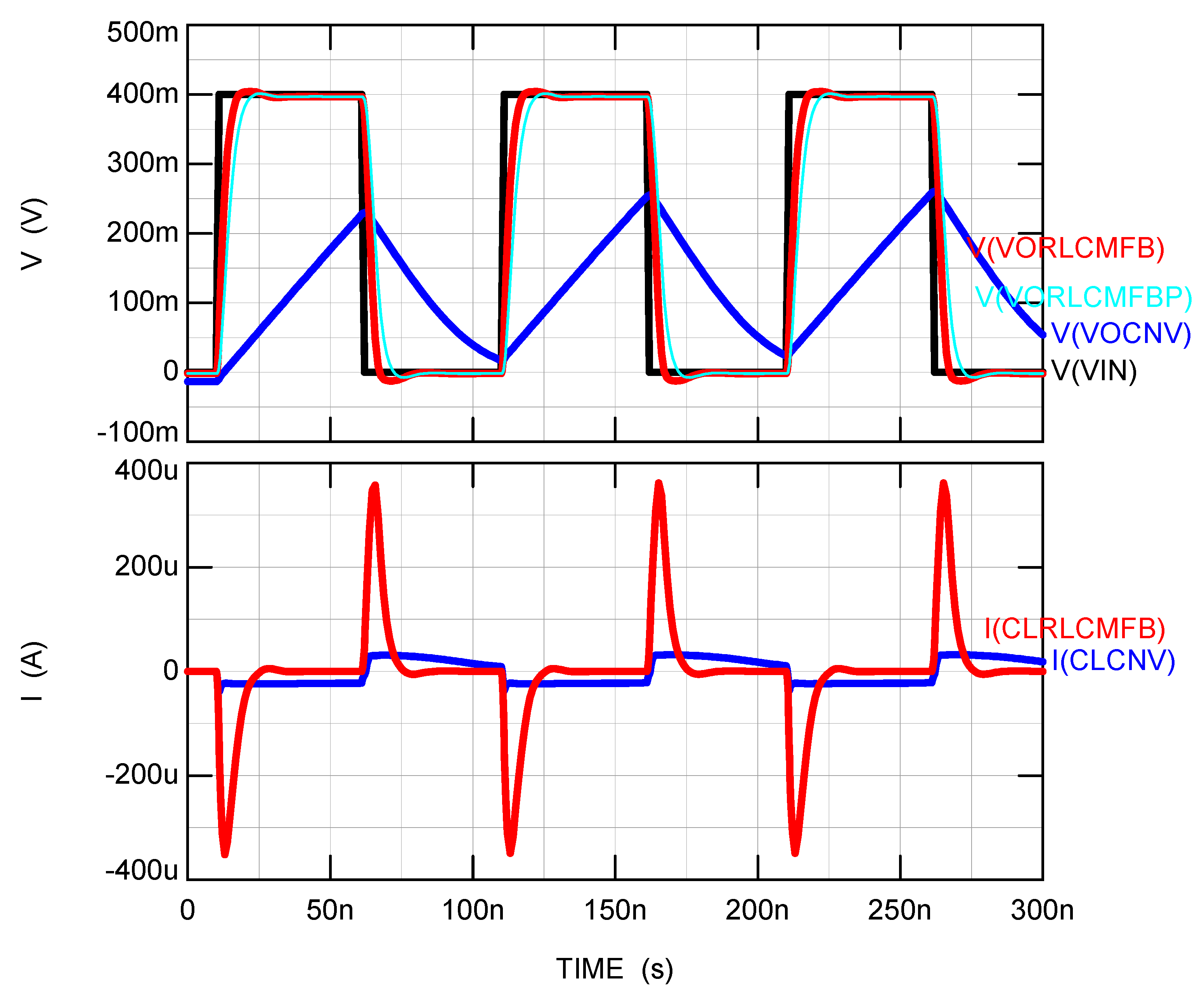
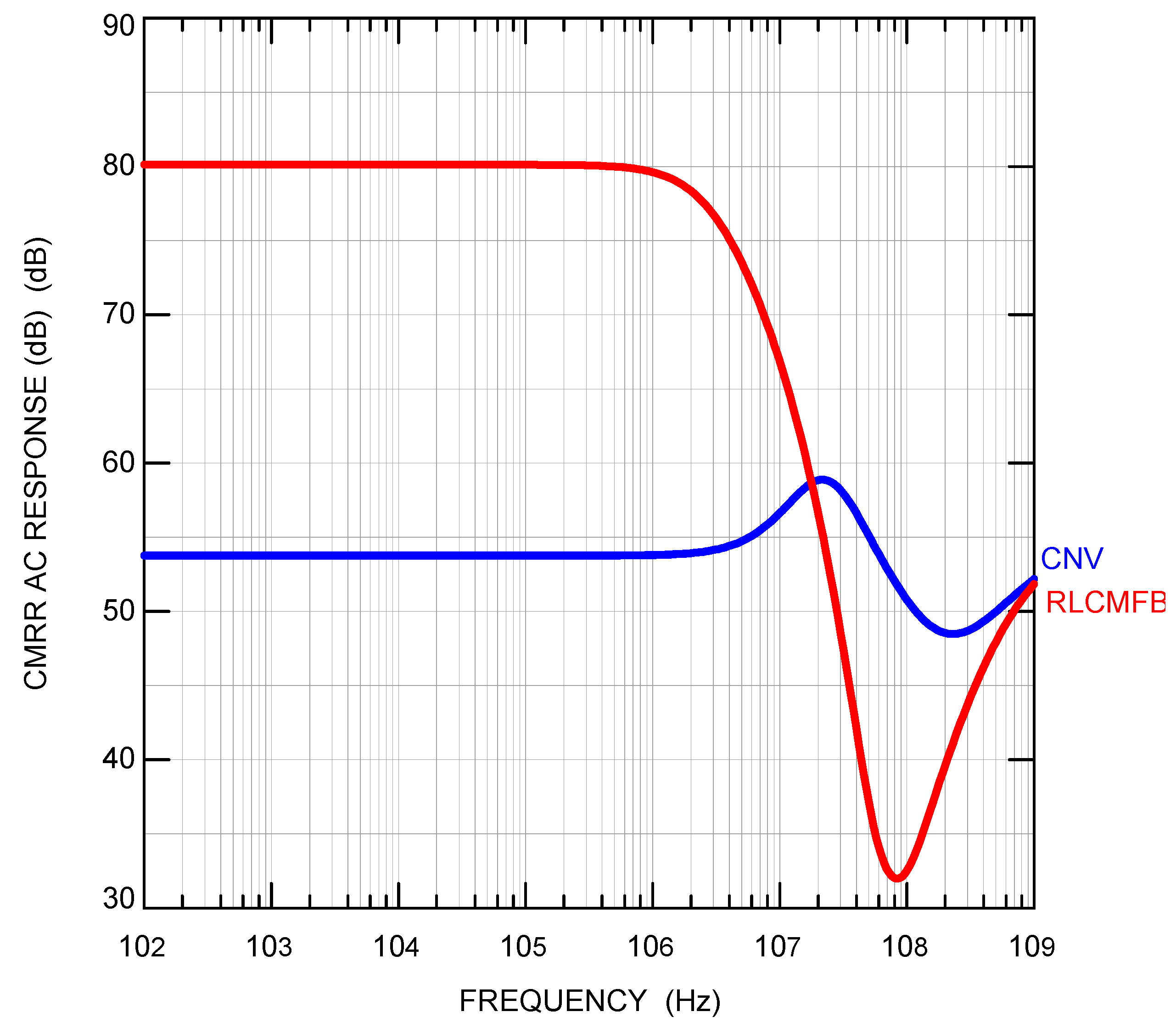
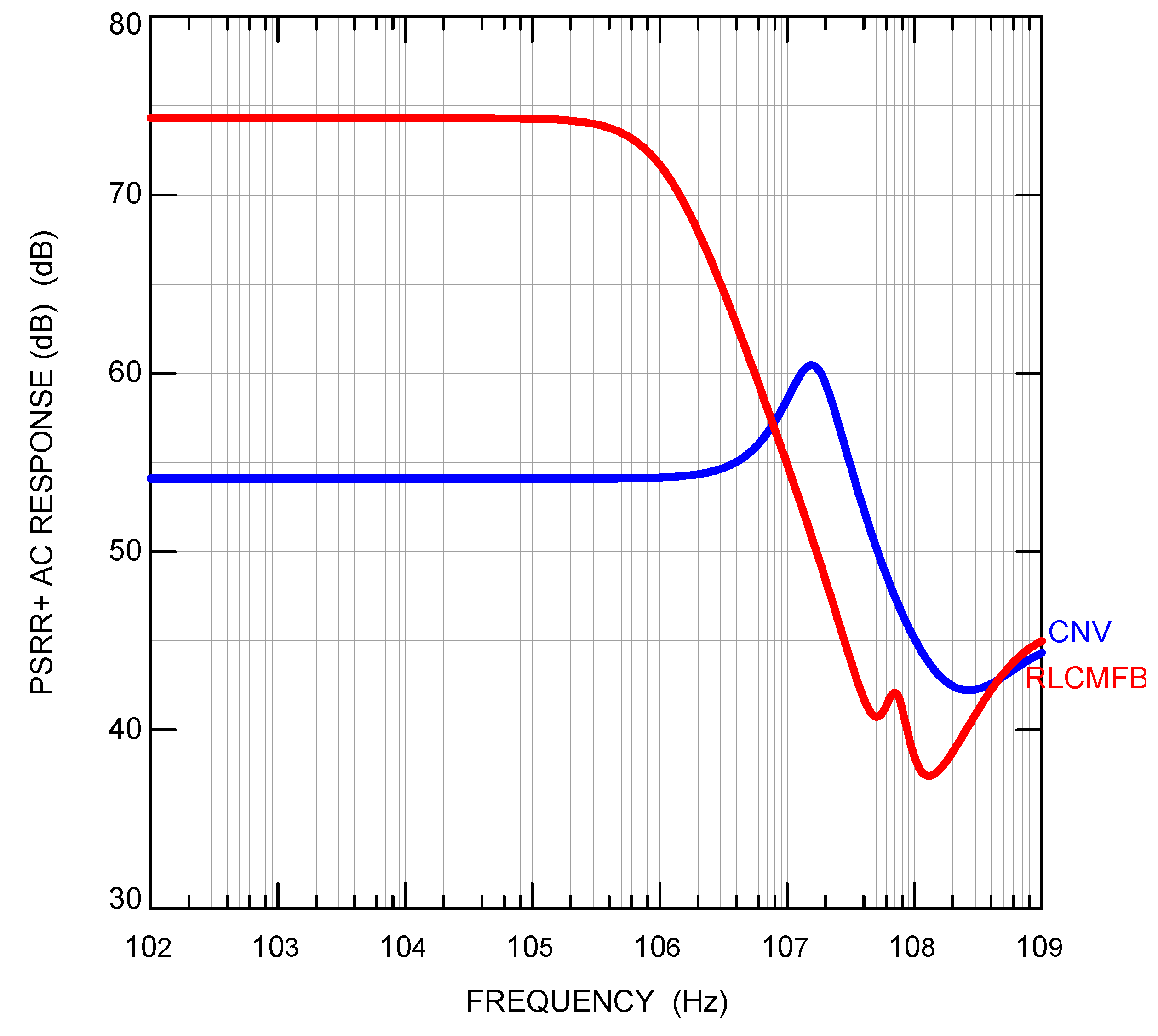
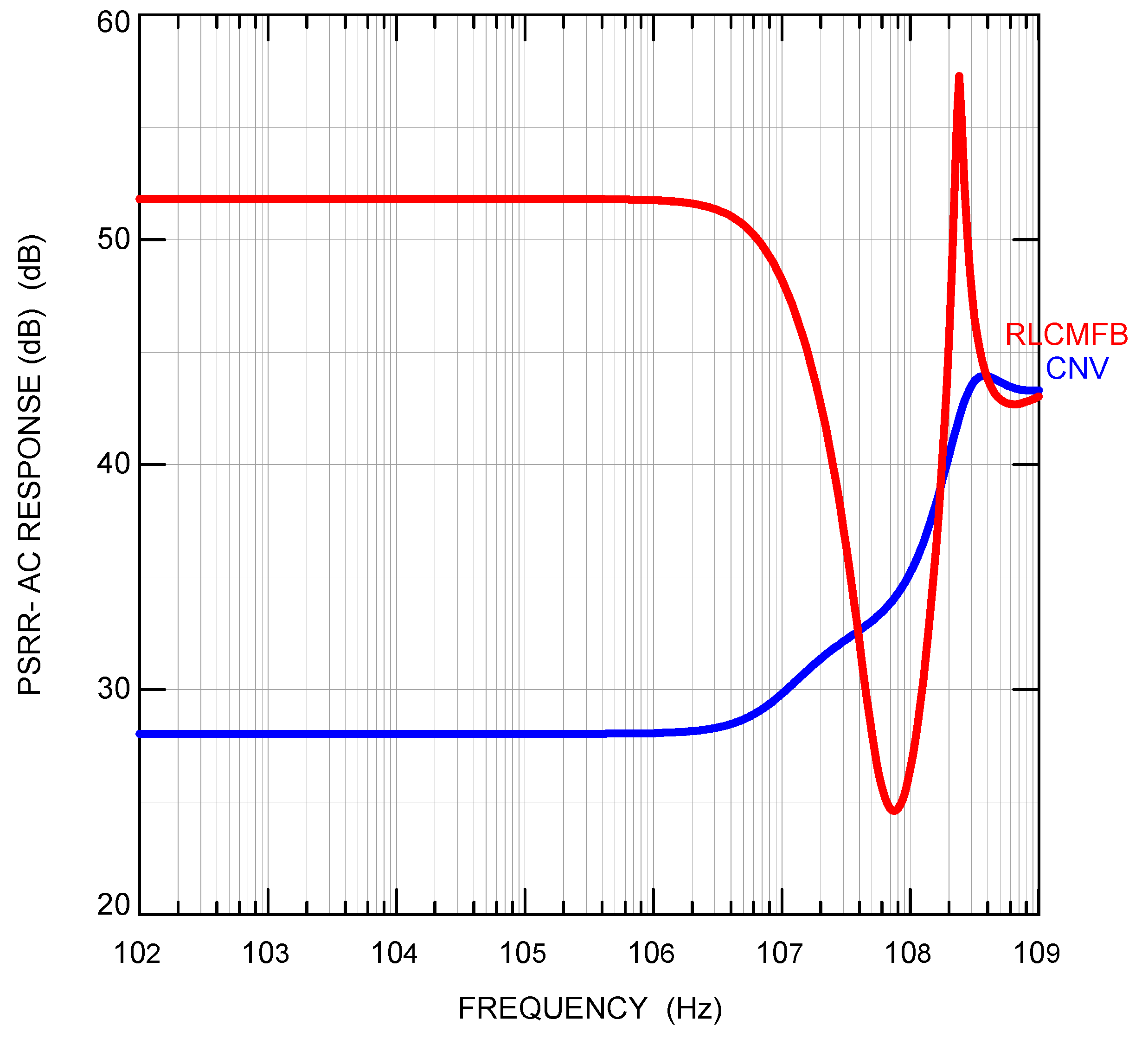
3. Comparison of Non-Cascoded Conventional and Resistive Local Common Mode Feedback OTAs

Figure 3a shows a non-cascoded OTA using a conventional three-mirror architecture where the input stage corresponds to the circuit of Figure 1b. Figure 3b shows an OTA with the RLCMFB input stage of Figure 1d. This circuit was reported originally in [1]. As mentioned in Section 1, cascode transistors are usually avoided (especially in the output stage of an OTA) due to severe output swing limitations in current CMOS technologies that use sub-volt supplies (unless transistors operate in subthreshold). As discussed below, the lack of cascode transistors leads to very low open loop gain for the circuit of Figure 3a. It is shown in this section that resistive local common mode feedback boosts essentially the open loop gain, the gain-bandwidth product, the slew rate, CMRR and PSRR of OTAs allowing sufficient phase margin (greater than 50°) if phase lead compensation is used. Both OTAs of Figure 3 have a dominant pole at the output node ωpout = 1/((ro3||ro4)CL) even with relatively low CL values. The open loop gain of the conventional OTA of Figure 3a is given by Aol = (gm1gm3/gm2) ro3||ro4 ≈ gmro/2 = Aint/2 which is only on the order of 10 to 25 (20–28 dB). Its gain-bandwidth product (in rad/s) is given by GB = Aolωpout = (gm1/CL) (gm3/gm2) = Mgm1/CL where M = gm3/gm2. The poles ωpa,b at nodes a and b of the circuit of Figure 3a are given by ωpa,b = gm2/Ca,b. These are high-frequency poles. For the common case CL >> Ca,b the poles ωpa,b satisfy the condition ωpa,b >> GB and the conventional OTA of Figure 3a has a phase margin close to 90o without compensation. The RLCMFB OTA of Figure 3b has an open loop gain Aol = gm1R′gm3ro3||ro4 = gm1R′Aint/2 = KenhAint/2 where Kenh = gmR′ is the gain enhancement factor introduced by the RLCMFB input stage and that for R′ >> ro1||ro2 takes a value Kenh = gm1ro1||ro2 = Aint/2. It has a gain-bandwidth product GB = Kenh gm3/CL which is also a factor of Kenh larger than the GB of the circuit of Figure 3a. Even for values R′ >> ro1||ro2 for which maximum Kenh is achieved, the poles at nodes a, b given by ωpa,b = 2/(roCa,b), have values that for the typical load capacitances CL >> Ca,b are close to GB in modern CMOS technologies. If necessary, their phase shift at the unity gain frequency can be partially compensated using phase lead compensation. This uses just a resistor Rs in series with the output terminal that introduces a left s-plane zero with value ωz = 1/(RsCL) in the open loop gain. The phase of the zero subtracts from the phase of poles ωpa,b at the unity gain frequency allowing sufficient phase margins PM > 50°.

Summary

In current CMOS technologies, the open loop gain and GB are enhanced by the factor Kenh by utilization of RLCMFB and even for large Kenh values it is possible to obtain sufficient phase margin using phase lead compensation. Miller (or two-stage) op-amps have a GB characterized by GB = gm1/Cc (in rad/s) where Cc is the Miller compensation capacitor that in a typical design is selected with a value Cc = CL in which case GB = gm1/CL. Notice that the OTA of Figure 3b has also a GB enhanced by the same factor Kenh with respect to the conventional Miller op-amp. The CMRR of the OTAs of Figure 3 corresponds approximately to CMRR = (gm12rotail)/(ΔR′/R′)~200(gm1R′)(gm2rotail) for the circuit of Figure 3b and CMRR~200 gm1rotail for the circuit of Figure 3a. It can be seen that CMRR is also a factor of Kenh higher for the circuit of Figure 3b than for the circuit of Figure 3a. Table 1 summarizes expressions for the performance characteristics of the OTAs in Figure 3.
Figure 4 shows simulations of the open loop response of the OTAs of Figure 3 in 130 nm CMOS technology with CL = 5pF, dual supply voltages VDD = −VSS = 0.6 V, IBIAS = 5 µA, R = 600 kΩ, Rs = 0.4 kΩ, W/L = 5/0.26 (µm/µm) for NMOS transistors and PMOS transistors. Tail and output transistors Mtail, M3P and M4P are scaled by a factor of k = 2, the left branch transistors, M3 and M4, are scaled by a factor of k = 0.5. It can be seen that the open loop gain and phase margin of the conventional OTA have values Aolcnv = 27 dB and PMcnv = 90.8°, the OTA with RLCMFB of Figure 3b has enhanced open loop gain AolRLCMFB = 50.3 dB and a phase margin PMRLCMFB = 62.2°. The open loop gain of the RLCMFB OTA is 23.1 dB higher than for the conventional OTA (a factor of 14.1 in magnitude). The dominant (output) pole for both OTAs (determined by CL) has a value of fpout = 380.2 kHz. The unity gain frequencies of the conventional and RLCMFB OTAs are at 8.77 MHz and 72.4 MHz (a factor of 8.32 higher). Notice that due to the utilization of phase lead compensation with Rs, the RLCMFB OTA of Figure 3b has approximately a one pole open loop response shifted upwards with respect to the response of the conventional OTA, and for this reason, open loop gain and unity gain enhancement factors are similar (11.4 and 8.9, respectively).
Figure 5 shows simulations of the closed loop voltage follower response. The bandwidths of the conventional and RLCMFB OTAs are 8.3 MHz and 72.4 MHz, respectively.
Figure 6 shows the transient pulse response (output voltages and load currents) of the circuits of Figure 3. The peak positive/peak negative load currents of the conventional and RLCMFB OTAs are 32/23 µA and 357/352 µA, respectively. The corresponding positive and negative slew rates are 71.4/70.4 V/µs and 6.4/4.6 V/µs, respectively. The SR of the RLCMFB OTA is approximately symmetrical and almost two orders of magnitude (a factor of 76.5) larger than the SR of the conventional OTA. Simulations of CMRR, positive and negative PSRR shown in Figure 7, Figure 8 and Figure 9 below were performed by introducing 2% mismatches in the W/L of M2 and M2P and in the R and W/L values.
Figure 7 shows the frequency response of CMRR of the circuits of Figure 3. It can be seen that the conventional and RLCMFB OTAs have CMRR values of 54 dB and 80 dB, respectively. Notice that the RLCMFB OTA shows an improvement of 26 dB in CMRR with respect to the conventional OTA.
Figure 8 shows the positive PSRR (with respect to VDD) of the circuits of Figure 3. The conventional OTA has a PSRR+ of 54.1 dB which is 20.2 dB lower than the PSRR+ of the RLCMFB OTA with a PSRR+ of 74.3 dB.
Figure 9 shows the negative PSRR of the circuits of Figure 3. The conventional OTA and RLCMFB OTAs have a negative PSRR− of 28 dB and 51.8 dB, respectively. The negative PSRR− enhancement of the RLCMFB OTA is 23.8 db in this case.
Table 2 shows a comparison of the performance characteristics of the conventional OTA and the RLCMFB OTA of Figure 3a and Figure 3b, respectively. It can be seen that the RLCMFB has essentially improved performance over the conventional OTA. Table 3 shows a comparison of the performance characteristics of the RLCMFB OTA of Figure 3b to the OTAS literature. It can be seen that the circuit of Figure 3b has higher small signal, large signal and global figures of merit (FOMSS, FOMLS and FOMGLB) than all other OTAS in Table 2 and also than the conventional OTA.
In [8,9,10,11,12,13,14,15,16,17,18,19,20,21,22,23,24,25,26,27,28,29,30,31,32,33,34,35,36,37,38,39,40,41,42,43,44,45,46,47] various applications of the resistive local common mode feedback technique to enhance circuit’s performance have been reported. Some of these applicatoins are discussed with detail in Section 4, Section 5 and Section 6 below.

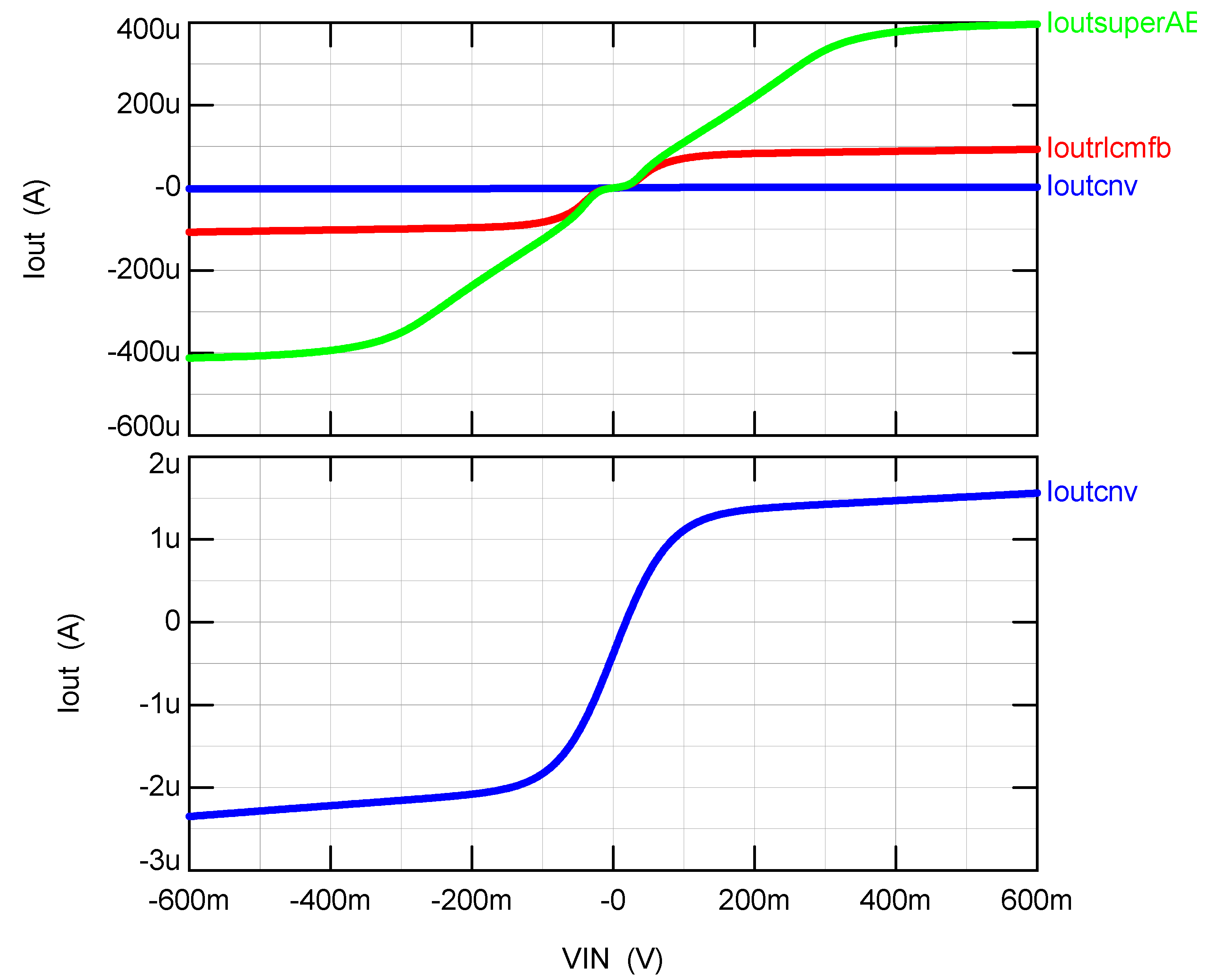
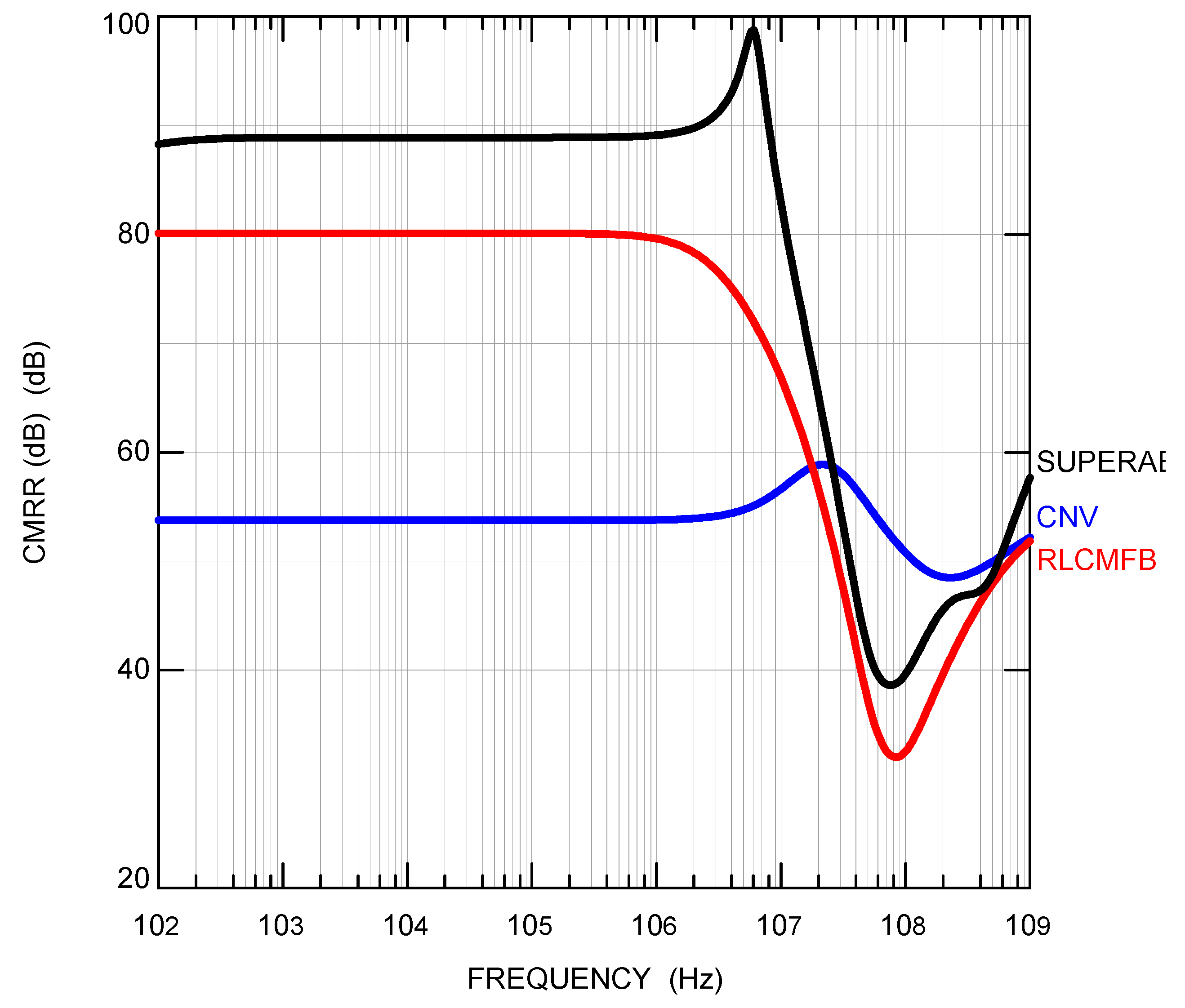
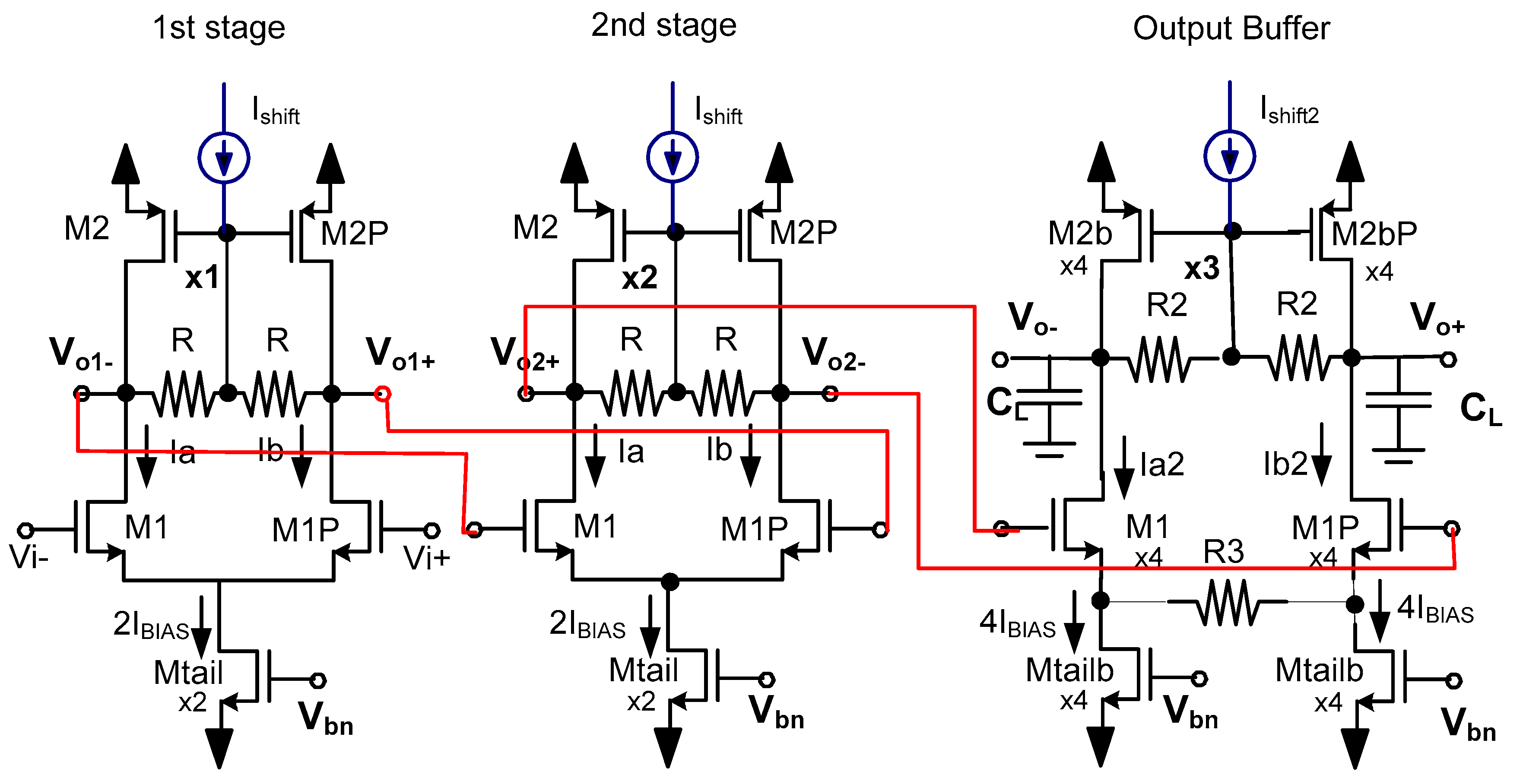
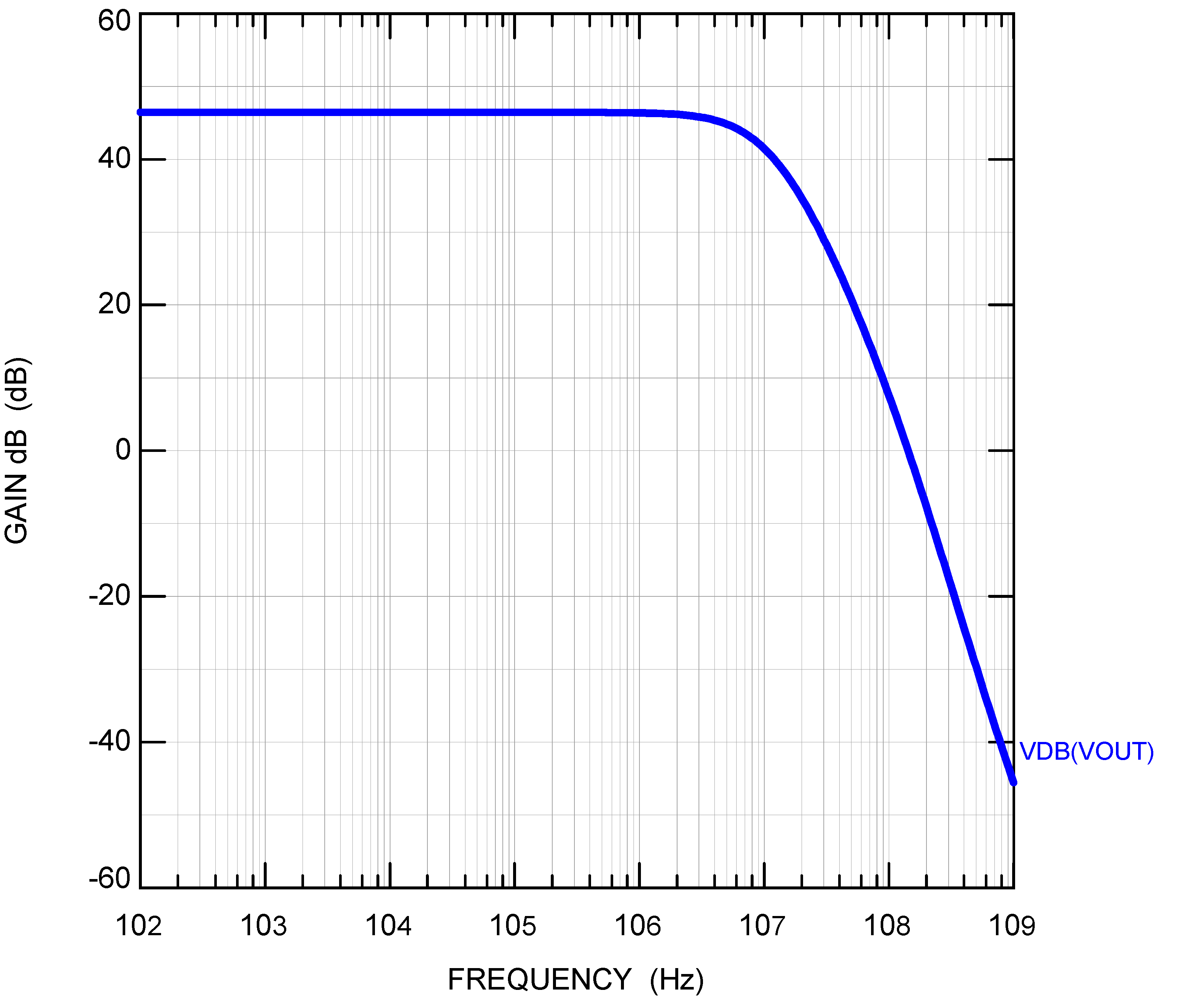
4. Super Class AB OTAs

The minimum of the positive and negative peak output currents determine the slew rate which is a measure of the large signal speed of an OTA while the gain-bandwidth product is a measure of the OTA speed for small signals. Both of them are important. There are situations where an OTA loaded with a large capacitance and/or low load resistance (that require large peak load currents) has a high bandwidth but it can handle only very small amplitude signals within its bandwidth because the slew rate, is very small. Super class AB OTAs can handle situations where an OTA is required to operate with large CL and/or low RL values (that require large peak output currents) with large amplitude within the full bandwidth of the OTA and maintaining a low quiescent power dissipation. In this section, we discuss the implementation of super class AB OTAs with enhanced open loop gain and GB using the combined effect of both gain and SR enhancement achieved with RLCMFB in conjunction with current boosting provided by a class AB differential pair. Several super class AB OTA architectures have been reported in [10,11,12,13,14,20,30,31,32,37,41]. They are characterized by very high current efficiency CE = Ioutpk/IBIAS (defined here as the ratio of the peak output current, Ioutpk to the bias current IBIAS) and by very large signal figures of merit FOMLS. Some of the reported structures have low open loop gain in current CMOS technologies but this limitation can be overcome by implementing them with RLCMFB. They deliver output load currents that can be 2 to 3 orders of magnitude larger than the bias current IBIAS and do not rely on the utilization of inverters connected to the output terminal (inverters at the output terminals have been used to achieve very large transient output currents. They are turned on when the op-amp is slewing but they can introduce spikes and distortion. Figure 10c shows a super class AB OTA derived from the RLCMFB OTA of Figure 3b by using a class AB differential pair according to the scheme reported in [48]. This is performed by replacing the tail current source Mtail of the differential pair with a Cascoded Flipped Voltage Follower. The Cascode Flipped Voltage Follower (FVF) was reported in [49]. It is a high-swing FVF that uses local negative feedback, by means of cascode transistor MC and Msink, to generate a very low impedance node at VG. Transistor MFVF operates as a floating battery VGSQ. The input common-mode detector (ICMDT) uses very large resistive elements Rlarge (Figure 10b). It is implemented with quasi-floating gate transistors [50] and small capacitances in parallel as shown in Figure 10b. These are used to detect the common mode input voltage ViCM of the OTA terminals Vi+ and Vi−. This voltage is applied at the gate of MFVF and is followed by VG causing node VG to follow common-mode input signals. The local feedback in the cascoded FVF causes VG performs as a very low impedance node (tens of Ωs) for differential signals and as a high impedance node (hundreds of kΩs) for common-mode input signals. The cascoded FVF (shown in red in Figure 10c) in conjunction with the ICMDT implements the scheme reported in [48] and shown in Figure 10a. M1 and M2 perform in this circuit as a class AB differential pair where transistors M1, M1P can generate currents Ia, Ib much larger than 2IBIAS while in the conventional differential pair transistors M1, MP can only generate maximum currents with value 2IBIAS. The class AB differential pair of Figure 10a,c has a small signal transconductance gain with value gm1 for differential signals and very low transconductance gain (<1/2rosink) for common mode signals.
The local negative feedback causes the class AB differential pair to have higher common mode rejection than the conventional differential pair. Under quiescent conditions, the gate-source voltage of MFVF is the same as that of, M1 and M1p, and sets their quiescent currents. For differential input signals Vd the gate-source voltages in M1 and M1P take values VGS1 = VGSQ + Vd/2 and VGS1P = VGSQ − Vd/2. This is not restricted to small signal operations. It also applies to large signals.
Figure 11 shows the transconductance characteristics Iout vs. Vin of the super class AB OTA of Figure 10 biased with IBIAS = 0.25 µA, for the RLCMFB OTA of Figure 3b and for the conventional OTA of Figure 3a. Simulations were performed in 130 nm CMOS technology with PMOS and NMOS transistor dimensions W/L = 5/0.26 (µm), output transistors scaled by a factor of 2, R = 2000 kΩ, Rs = 2 kΩ CL = 5 pF C = 1pF, VDD = −VSS = 0.6 V applying complementary input signals Vi+ = Vin/2, Vi− = −Vin/2 and with the OTA outputs connected to ground. It can be seen that the super class AB OTA delivers ±400 μA peak output currents, the RLCMFB OTA delivers ±100 µA peak output currents while the conventional OTA delivers only +1.5 µA and −2.5 µA peak output currents. The open loop gains of the super class AB and the RLCMFB OTAs are identical to those shown in Figure 4 (in red) and are not shown for the sake of space.
Figure 12 shows the CMRR frequency response of the same circuits. The OTAs were biased in this case with IBIAS = 5 μA, a 1% mismatch in the W/L of transistors and in R values was introduced to mimic fabrication mismatches and obtain realistic values of CMRR. The CMRR of the super class AB OTA, the RLCMFB OTA and the conventional OTA are 89 dB, 80 dB and 54 dB, respectively. The increased CMRR of the super class AB OTA is caused by the local feedback in the class AB DP. This increases the effective impedance for common mode signals at node VG by approximately a factor of 2.8 (or 9 dB).

5. Feedforward Amplifiers

The RLCMFB differential pair of Figure 1d can be also used to implement feedforward amplifiers with high gain and bandwidth. Figure 13 shows the scheme of a two-stage feedforward amplifier followed by an output buffering stage. The first two cascaded sections have a gain A1,2 = gmR′ and bandwidth (in Hz) BW1,2 ≈ (1/2π) (1/(R′Ca,b)). These two stages correspond to the DPs with RLCMFB of Figure 1d. The output buffer (with close to unity gain) is used to drive the capacitive load CL. It has a differential pair with resistive gain degeneration R3 and common mode feedback resistive loads R2. It has a gain Abuf = (R2||ro2)/((1/gm1 + R3/2) and a bandwidth (in Hz) BWbuf ≈ (1/2π)(1/(R2CL)). The current sources, Ishift and Ishiftbuf, are used to obtain quiescent values at the output nodes VoQ1,2 = VDD − VSGQ2 − RIshift/2, VoQbuf = VDD − VSGQ2buf-RIshiftbuf/2 close to zero Volts to maximize output signal swing. It is possible to achieve higher gains by adding more gains stages. This circuit does not require compensation since it does not use global feedback. The amplified input DC offset can saturate the outputs. In order to prevent this, the gain stages of this circuit should be AC coupled or if a wideband gain starting from very low frequencies (close to DC) is required, a servo-loop (similar to the one reported in [51]), that attenuates gain for DC signals, should be connected between the output of the second stage and the input of the first stage.
The circuit of Figure 13 was simulated in 130 nm CMOS technology with IBIAS = 5 µA in the first and second stages and 20 µA in the output buffer stage. Dual supplies VDD = −VSS = 0.6 V, and dimensions for PMOS and NMOS transistors W/L = 5/0.26 (µm) were used. The dimensions and bias currents of the output stage transistors were scaled by a factor of 4. Values R = 300 kΩ, R2 = 8.5 kΩ, R3 = 10 kΩ and CL = 2 pF were used. Figure 14 shows the frequency response of the circuit. Figure 15a shows the transient response to a triangular wavefrom. Figure 15b shows the pulse reponse. The gain of the circuit is A = 46.4 dB, the bandwidth BW = 7.2 MHz and the power dissipation Pdis = 72 µW. This corresponds to a small signal figure of merit FOMSS = A BW CL/Pdis = 40 MHzpF/µW.

6. Other Applications

Since the RLCMFB technique to increase slew rate and gain was reported in [1], as well as other applications in [8,9] many other applications that achieve performance enhancement in analog circuits using this technique have been reported [10,11,12,13,14,15,16,17,18,19,20,21,22,23,24,25,26,27,28,29,30,31,32,33,34,35,36,37,38,39,40,41,42,43,44,45,46,47]. These include the utilization of capacitive (instead of resistive) local common mode feedback using floating gate transistors as shown in Figure 16b [12,15,16,22,23]. This is in order to reduce the silicon area if resistors R >> ro1||ro2 are required to achieve maximum Kenh values. Ultra high gain op-amps [39], Bulk driven and multistage operational amplifiers [29,35,45], rail-to-rail sample and hold circuits [18], buffers for high-density microelectrode arrays [24], LDOs [27], delta-sigma modulators [34], VGAs [36], gain and GB improved common mode feedback networks used in fully differential op-amps [30], etc. Other possible applications include the implementation of high frequency, high Q bandpass amplifiers using inductive common mode feedback (Figure 16c) where resistors are replaced by inductors and capacitors Ca, Cb by varactors CL to achieve tunable resonant frequencies ωres = 1/(LCL)1/2 in a multistage feedforward configuration similar to the one shown in Figure 13.

7. Conclusions

In this paper, a review of the resistive local common mode feedback technique and its application to improve amplifier’s performance was presented. It was shown that this technique is especially appropriate in current deep submicrometer CMOS technologies to essentially improve open loop gain, GB, SR, CMRR and PSRR of amplifiers without increasing power dissipation or supply requirements and by adding small additional circuit complexity.

Author Contributions

Conceptualization, J.R.-A., A.J.L.-M., R.G.C., A.T. and J.H.-C.; methodology, J.R.-A., A.J.L.-M., R.G.C., A.T. and J.H.-C.; validation, J.R.-A., A.J.L.-M., R.G.C., A.T. and J.H.-C.; formal analysis, J.R.-A., A.J.L.-M., R.G.C. and A.T.; writing—original draft preparation, J.R.-A., A.J.L.-M. and R.G.C.; writing—review and editing, J.R.-A., A.J.L.-M. and R.G.C.; visualization, J.R.-A., A.J.L.-M., R.G.C. and A.T.; supervision, J.R.-A., A.J.L.-M., R.G.C. and A.T.; project administration J.R.-A., A.J.L.-M., R.G.C. and A.T.; funding acquisition, A.J.L.-M., R.G.C. and A.T. All authors have read and agreed to the published version of the manuscript.

Funding

This research was partially funded by AEI/FEDER, grant number PID2019-107258RB-C31 and in part by the Andalusia Economy, Knowledge, Enterprise and University Council under Project P18-FR-4317.

Institutional Review Board Statement

Not applicable.

Informed Consent Statement

Not applicable.

Data Availability Statement

Not applicable.

Conflicts of Interest

The authors declare no conflict of interest. The funders had no role in the design of the study; in the collection, analyses, or interpretation of data; in the writing of the manuscript; or in the decision to publish the results.

References

  1. Ramirez-Angulo, J.; Holmes, M. Simple technique using Local CMFB to enhance Slew Rate and bandwidth of one-Stage CMOS op-amps. Electron. Lett. 2002, 38, 1409–1411. [Google Scholar] [CrossRef]
  2. Ragheb, A.N.; Kim, H. Ultra-low power OTA based on bias recycling and subthreshold operation with phase margin enhancement. Microelectron. J. 2017, 60, 94–101. [Google Scholar] [CrossRef]
  3. Feizbakhsh, S.V.; Yosefi, G. An enhanced fast slew rate recycling folded cascode Op-Amp with general improvement in 180 nm CMOS process. AEU-Int. J. Electron. Commun. 2019, 101, 200–217. [Google Scholar] [CrossRef]
  4. Kuo, P.-Y.; Tsai, S.-D. An Enhanced Scheme of Multi-Stage Amplifier with High-Speed High-Gain Blocks and Recycling Frequency Cascode Circuitry to Improve Gain-Bandwidth and Slew Rate. IEEE Access 2019, 7, 130820–130829. [Google Scholar] [CrossRef]
  5. Kuo, P.-Y.; Liao, H.-W.; Peng, J.-S. An Improved Recycling Folded-Cascode Amplifier with High Unity-Gain Frequency. In Proceedings of the 2020 IEEE International Conference on Consumer Electronics-Taiwan (ICCE-Taiwan), Taoyuan, Taiwan, 28–30 September 2020; pp. 1–2. [Google Scholar]
  6. Kim, J.; Song, S.; Roh, J. A High Slew-Rate Enhancement Class-AB Operational Transconductance Amplifier (OTA) for Switched-Capacitor (SC) Applications. IEEE Access 2020, 8, 226167–226175. [Google Scholar] [CrossRef]
  7. Nandi, G.; Yadav, S.; Kondekar, P. A Fast Settling, High Slew Rate CMOS Recycling Folded Cascode Operational Transconductance Amplifier (OTA) for High Speed Applications. In Proceedings of the 2021 12th International Conference on Computing Communication and Networking Technologies (ICCCNT), Kharagpur, India, 6–8 July 2021; pp. 1–6. [Google Scholar]
  8. Harrison, J.; Weste, N. 350 MHz opamp-RC filter in 0.18 µm CMOS. Electron. Lett. 2002, 38, 259–260. [Google Scholar] [CrossRef] [Green Version]
  9. Harrison, J.; Weste, N. A 500 MHz CMOS anti-alias filter using feed-forward op-amps with local common-mode feedback. In Proceedings of the IEEE International Solid-State Circuits Conference, San Francisco, CA, USA, 13 February 2003; pp. 132–133. [Google Scholar]
  10. Baswa, S.; Lopez-Martin, A.J.; Ramirez-Angulo, J.; Carvajal, R.G. Low-voltage Micropower Super Class AB CMOS OTA. Electron. Lett. 2004, 40, 216–217. [Google Scholar] [CrossRef]
  11. Schlogl, F.; Zimmermann, H. 1.5 GHz OPAMP in 120 nm digital CMOS. In Proceedings of the 30th European Solid-State Circuits Conference, Leuven, Belgium, 21–23 September 2004; pp. 239–242. [Google Scholar]
  12. Chawla, R.; Serrano, G.; Allen, D.J.; Pereira, A.W.; Hasler, P.E. Fully differential floating-gate programmable OTAs with novel common-mode feedback. In Proceedings of the IEEE International Symposium on Circuits and Systems, Vancouver, CA, USA, pp. I-817–I-820., 23–26 May 2004. [Google Scholar]
  13. Lopez-Martin, A.J.; Baswa, S.; Ramirez-Angulo, J.; Carvajal, R.G. Low-Voltage Super class AB CMOS OTA cells with very high slew rate and power efficiency. IEEE J. Solid-State Circuits 2005, 40, 1068–1077. [Google Scholar] [CrossRef]
  14. Baswa, S.; Ramirez-Angulo, J.; Lopez-Martin, A.J.; Carvajal, R.G.; Bikumandla, M. Rail-to-Rail super Class AB CMOS Operational Amplifiers. Electron. Lett. 2005, 41, 1–2. [Google Scholar] [CrossRef]
  15. Chawla, R.; Serrano, G.; Allen, D.; Hasler, P. Programmable floating-gate second-order sections for Gm-C filter applications. In Proceedings of the 48th Midwest Symposium on Circuits and Systems, Cincinnati, OH, USA, 21–23 August 2005; pp. 1649–1652. [Google Scholar]
  16. Chawla, R.; Adil, F.; Serrano, G.; Hasler, P.E. Programmable GmC Filters Using Floating-Gate Operational Transconductance Amplifiers. IEEE Trans. Circuits Syst. I Regul. Pap. 2007, 54, 481–491. [Google Scholar] [CrossRef]
  17. Motlak, H.J.; Ahmad, S.N. A Novel Design Technique of One Stage CMOS OTA For High Frequency Applications. Frequenz 2007, 61, 182–188. [Google Scholar] [CrossRef]
  18. Ramirez-Angulo, J.; Lujan-Martinez, C.; Rubia-Marcos, C.; Carvajal, R.G.; Lopez-Martin, A.J. Rail to Rail Fully Differential Sample and Hold Based on Clocked Differential Difference Amplifier Using Resistive Local Common Mode Feedback. IET Electron. Lett. 2008, 44, 656–658. [Google Scholar] [CrossRef]
  19. Ramirez-Angulo, J.; Carvajal, R.G.; Lopez-Martin, A.J. High slew rate two stage A/AB and AB/AB op-amps with phase lead compensation at output node and local common mode feedback. In Proceedings of the IEEE International Symposium on Circuits and Systems, Seattle DC, USA, 21–23 May 2008; pp. 288–291. [Google Scholar]
  20. Grasso, A.D.; Monsurrò, P.; Pennisi, S.; Scotti, G.; Trifiletti, A. Analysis and Implementation of a Minimum-Supply Body-Biased CMOS Differential Amplifier Cell. IEEE Trans. Very Large Scale Integr. (Vlsi) Syst. 2009, 17, 172–180. [Google Scholar] [CrossRef]
  21. Mehra, A.; Gupta, A.; Patil, S.; Mehra, A.; Sahoo, S.K. A Novel Dynamic Current Boosting Technique for Enhancement of Settling Time and Elimination of Slewing of CMOS Amplifiers. In Proceedings of the 2009 International Conference on Advances in Recent Technologies in Communication and Computing, Kottayam, India, 27–28 October2009; pp. 115–117. [Google Scholar]
  22. Ramirez-Angulo, J.; Nargis, A.; Carvajal, R.G.; Lopez-Martin, A. CMOS Operational Amplifiers with Continuous-Time Capacitive Common Mode Feedback. In Proceedings of the IEEE ISCAS 2010, Paris, France, 29 May–2 June 2010; pp. 1280–1283. [Google Scholar]
  23. Nargis, A. CMOS Operational Amplifiers with continuous time Capacitive Common Mode Feedback. Master’s Thesis, New Mexico State University, Las Cruces, NM, USA, 2010. [Google Scholar]
  24. Heer, L.F.; Frey, U.; Bakkum, D.J.; Hierlemann, A. Compact Voltage and Current Stimulation Buffer for High-Density Microelectrode Arrays. IEEE Trans. Biomed. Circuits Syst. 2010, 4, 372–378. [Google Scholar]
  25. Chen, Y.; He, X.-y.; Pun, K.-p. A 0.5V amplifier with adaptive CMFB compensation for a 2-1 cascade CT Delta Sigma modulator. In Proceedings of the 2010 IEEE International Conference of Electron Devices and Solid-State Circuits (EDSSC), Hong Kong, China, 15–17 December 2010; pp. 1–4. [Google Scholar]
  26. Huang, B.; Xu, L.; Chen, D. Slew rate enhancement via excessive transient feedback. IET Electron. Lett. 2013, 49, 930–932. [Google Scholar] [CrossRef]
  27. Fathipour, R.; Saberkari, A.; Martinez, H.; Alarcón, E. High slew rate current mode transconductance error amplifier for low quiescent current output-capacitorless CMOS LDO regulator. Integr. VLSI J. 2014, 47, 204–212. [Google Scholar] [CrossRef]
  28. Perez-Nicoli, P.; Veirano, F.; Lisboa, P.C.; Silveira, F. Low-power operational transconductance amplifier with slew-rate enhancement based on non-linear current mirror. J. Analog. Integr. Circuits Signal Process. 2016, 89, 521–529. [Google Scholar] [CrossRef]
  29. Cabrera-Bernal, E.; Pennisi, S.; Grasso, A.D.; Torralba, A.; Carvajal, R.G. 0.7-V Three-Stage Class-AB CMOS Operational Transconductance Amplifier. IEEE Trans. Circuits Syst. I Regul. Pap. 2016, 63, 1807–1815. [Google Scholar] [CrossRef]
  30. Garde, M.P.; Lopez-Martin, A.J.; Ramirez-Angulo, J. Improved common-mode feedback based on LCMFB techniques. In Proceedings of the 2017 13th Conference on Ph.D. Research in Microelectronics and Electronics (PRIME), Taormina, Italy, 12–15 June 2017; pp. 277–280. [Google Scholar]
  31. Algueta-Miguel, J.M.; Lopez-Martin, A.; Pilar Garde, M.; De La Cruz, C.A.; Ramirez-Angulo, J. ±0.5 V 15 μW Recycling Folded Cascode Amplifier with 34,767 MHzpF/mA. IEEE Solid State Circuits Lett. 2018, 1, 170–173. [Google Scholar] [CrossRef]
  32. Garde, M.P.; Lopez-Martin, A.; Carvajal, R.G.; Ramírez-Angulo, J. Super Class-AB Recycling Folded Cascode OTA. IEEE J. Solid-State Circuits 2018, 53, 2614–2623. [Google Scholar] [CrossRef]
  33. Pourashraf, S.; Ramirez-Angulo, J.; Lopez-Martin, A.J.; González-Carvajal, R. A Highly Efficient Composite Class-AB-AB Miller Op-Amp With High Gain and Stable From 15 pF Up To Very Large Capacitive Loads. IEEE Trans. Very Large Scale Integr. (VLSI) Syst. 2018, 26, 2061–2072. [Google Scholar] [CrossRef]
  34. Chen, Y.; Wang, X.; Zhang, Y.; Pun, K.P. A 0.4-V 0.2 pJ/step 90-dB SNDR 20-kHz CT delta-sigma modulator using class-AB amplifier with a novel local common-mode feedback. IEICE Electron. Express 2019, 16, 20190170. [Google Scholar] [CrossRef] [Green Version]
  35. Paul, A.; Ramírez-Angulo, J.; López-Martín, A.J.; Carvajal, R.G.; Rocha-Pérez, J.M. Pseudo-Three-Stage Miller Op-Amp with Enhanced Small-Signal and Large-Signal Performance. IEEE Trans. Very Large Scale Integr. (VLSI) Syst. 2019, 27, 2246–2259. [Google Scholar] [CrossRef]
  36. Rico-Aniles, H.D.; Ramírez-Angulo, J.; Rocha-Pérez, J.M.; López-Martín, A.J.; Carvajal, R.G. Low-Voltage 0.81mW, 1-32 CMOS VGA with 5% Bandwidth Variations and -38dB DC Rejection. IEEE Access 2020, 8, 106310–106321. [Google Scholar] [CrossRef]
  37. Yen, A.; Blalock, B.J. A High Slew Rate, Low Power, Compact Operational Amplifier Based on the Super-Class AB Recycling Folded Cascode. In Proceedings of the IEEE 63rd International Midwest Symposium on Circuits and Systems (MWSCAS), Springfield, MA, USA, 9–12 August 2020; pp. 9–12. [Google Scholar]
  38. Renteria-Pinon, M.; Ramirez-Angulo, J.; Diaz-Sanchez, A. Simple Scheme for the Implementation of Low Voltage Fully Differential Amplifiers without Output Common-Mode Feedback Network. MDPI J. Low Power Electron. Appl. 2020, 10, 34. [Google Scholar] [CrossRef]
  39. Paul, A.; Ramírez-Angulo, J.; Díaz-Sánchez, A.; López-Martín, A.J.; Carvajal, R.G.; Li, F.X. Super-Gain-Boosted AB-AB Fully Differential Miller Op-Amp with 156 dB Open-loop Gain and 174MV/V MHZ pF/µW Figure of Merit in 130 nm CMOS Technology. IEEE Access 2021, 9, 57603–57617. [Google Scholar] [CrossRef]
  40. Paul, A.; Renteria-Pinon, M.; Ramirez-Angulo, J.; Bolaños-Pérez, R.; Vázquez-Leal, H.; Huerta-Chua, J.; Diaz-Sánchez, A. Implementation of Power-Efficient Class AB Miller Amplifiers Using Resistive Local Common-Mode Feedback. J. Low Power Electron. Appl. 2021, 11, 31. [Google Scholar] [CrossRef]
  41. Beloso-Legarra, J.; de la Cruz-Blas, C.A.; Lopez-Martin, A.J.; Ramirez-Angulo, J. Gain-Boosted Super Class AB OTAs Based on Nested Local Feedback. IEEE Trans. Circuits Syst. I Regul. Pap. 2021, 68, 3562–3573. [Google Scholar] [CrossRef]
  42. Sagar, G.N.; Kumar, B.A.; Reddy, G.B.S. Low-Power High-Gain Op-Amp With Cascoded Current Mirror Loads. In Proceedings of the 2021 5th International Conference on Electronics, Communication and Aerospace Technology (ICECA), Coimbatore, Tamil Nadu, India, 2–4 December 2021; pp. 179–186. [Google Scholar]
  43. Sagar, G.N.; Kumar, B.A.; Reddy, G.B.S. High Gain and Stable Class AB-AB Miller Op-Amp for Large Capacitive Loads Ranging From 15pF. In Proceedings of the 2021 5th International Conference on Trends in Electronics and Informatics (ICOEI), Tirunelveli, Tamilnadu, India, 3–5 June 2021; pp. 19–25. [Google Scholar]
  44. Paul, A.; Ramirez-Angulo, J.; Huerta-Chua, J.; Vazquez-Leal, H.; Diaz Sanchez, A. Fully Differential Miller Op-amp with Enhanced Large and Small Signal Figures of Merit. J. Low Power Electron. Appl. 2022, 12, 9. [Google Scholar] [CrossRef]
  45. Gangeni, M.; Ramirez-Angulo, J.; Vazquez-Leal, H.; Huerta-Chua, J.; Lopez-Martin, A.J.; Carvajal, R.G. ±0.3V Bulk-Driven Fully Differential Buffer with High Figures of Merit. J. Low Power Electron. Appl. 2022, 12, 35. [Google Scholar] [CrossRef]
  46. Yu, Z.; Xiao, Z.; Liyuan, D. A Local Positive Feedback Loop-Reused Technique for Enhancing Performance of Folded Cascode Amplifier. In Proceedings of the 2022 IEEE 4th International Conference on Circuits and Systems (ICCS), Chengdu, China, 23–26 September 2022; pp. 164–167. [Google Scholar]
  47. Ramirez-Angulo, J.; Diaz-Armendariz, A.; Molinar-Solis, J.E.; Diaz-Sanchez, A.; Huerta-Chua, J. Simple Technique to essentially improve the performance of one stage op-amps in deep submicrometer CMOS technology. J. Low Power Electron. Appl. 2023, 13, 4. [Google Scholar] [CrossRef]
  48. Ramirez-Angulo, J.; Gonzalez-Carvajal, R.; Torralba, A.; Nieva, C. A new Class AB differential Input stage for implementation of low voltage high slew rate op-amps and linear transconductors. In Proceedings of the IEEE International Symposium on Circuits an Systems, Sidney, Australia, 6–9 May 2001; pp. I-671–I-674. [Google Scholar]
  49. Gupta, S.; Padilla, I.; Ramirez-Angulo, J.; Torralba, A.; Jimenez, M. Comparison of Conventional and New Flipped Voltage Follower Structures. In Proceedings of the 2005 IEEE Midwest Symposium on Circuits and Systems, Cincinnati, OH, USA, 21–23 August 2005; pp. 1151–1154. [Google Scholar]
  50. Ramirez-Angulo, J.; Urquidi, C.; Carvajal, R.G.; Lopez-Martin, A.J. A new Family of Very Low-Voltage Analog Circuits Based on Quasi Floating Gate Transistors. IEEE Trans. Circuits Syst. II 2003, 50, 214–220. [Google Scholar] [CrossRef]
  51. Pourashraf, S.; Ramírez-Angulo, J.; Lopez-Martin, A.J.; Carvajal, R.G. Op-Amp Approaches for Bandpass VGAs with Constant Bandwidth. IEEE TCAS-II 2018, 65, 1144–1148. [Google Scholar]
Figure 1. (a) Conventional differential pair with resistive load. (b) Differential pair with diode-connected load and optional positive feedback load (c) Differential pair with current source active loads (d) Differential pair with resistive local common mode feedback load. This is a figure. Schemes follow the same formatting.
Eng 04 00047 g001
Figure 2. Operation of differential pair with RLCMFB: (a) Quiescent operation. (b) Operation with complementary differential inputs. (c) Operation with common mode inputs.
Eng 04 00047 g002
Figure 3. One stage non-cascoded OTAS. (a) Conventional three current mirror OTA. (b) OTA with resistive local common mode feedback in input stage.
Eng 04 00047 g003
Figure 4. Open loop response AC responses of circuits of Figure 3.
Eng 04 00047 g004
Figure 5. Voltage follower AC responses of circuits of Figure 3.
Eng 04 00047 g005
Figure 6. Transient response of circuits of Figure 3. Top: input and output voltages, bottom: output currents.
Eng 04 00047 g006
Figure 7. CMRR response of circuits of Figure 3.
Eng 04 00047 g007
Figure 8. Positive PSRR of circuits of Figure 3.
Eng 04 00047 g008
Figure 9. Negative PSRR of the circuits of Figure 3.
Eng 04 00047 g009
Figure 10. High gain super class AB OTA using the combined current boosting effect of RLCMFB and of class AB differential pair. (a) Conceptual implementation of class AB DP using the floating battery. (b) Implementation of very large resistive elements using quasi-floating gate transistors. (c) Transistor level implementation of super class AB OTA.
Eng 04 00047 g010
Figure 11. Transconductance characteristics of conventional OTA of Figure 3a (blue trace), RLCMFB OTA of Figure 3b (red trace) and super class AB OTA of Figure 10 (green trace).
Eng 04 00047 g011
Figure 12. CMRR of super class AB OTA of Figure 10, of RLCMFB OTA of Figure 3b and of conventional OTA of Figure 3a simulated with IBIAS = 5 µA.
Eng 04 00047 g012
Figure 13. Feedforward high gain multistage amplifier consisting of two cascaded gain stages and a buffering output stage.
Eng 04 00047 g013
Figure 14. Frequency response of circuit of Figure 13.
Eng 04 00047 g014
Figure 15. Transient response of circuit of Figure 13 (a) with triangular input signal, (b) with pulse input signal.
Eng 04 00047 g015
Figure 16. (a) Differential pair with resistive local common mode feedback. (b) Differential pair with capacitive local common mode feedback. (c) Differential pair with inductive local common mode feedback.
Eng 04 00047 g016
Table 1. Basic performance characteristics of OTAs of Figure 3.
Parameter Expression Conventional OTA of Figure 3aOTA with RLCMFB of Figure 3b
Aol (V/V)(gm1gm3/gm2) ro3||ro4~Aint/2gm1R′gm3 (ro3||ro4)~(Aint/2)2
GB (rad/s)(gm1/CL) (gm3/gm2)~gm/CLgm1R′gm3/CL)~Aintgm/CL
SR (V/s)2IBIAS/CLMIBIAS(IBIASR/VDSSat)2/CL
CMRR ~200 gm1rotail~200(gm1R′)(gm2rotail)
Table 2. Comparison of performance characteristics of OTAs of Figure 3.
Conventional OTA Figure 3aRLCMFB OTA Figure 3b
CL (pF), Rs(kΩ)5 pf, 05 pF, 0.4
W/L PMOS, and NMOS (µm/µm)5/0.265/0.26
Vos (mV)−12.40.9
Aol (dB)27.250.3
PM (°)90.862.2
Pdiss (uW)3030
fpout (MHz)0.38020.3802
fu (MHz)8.772.4
Pdis(uW)3030
BWVF8.375.9
GB (MHz)8.7124
SR+/SR− (V/µs)6.4/4.671.4/70.4
CMRR (dB)5480
PSRR+ (dB)54.174.3
PSRR− (dB)2851.8
Input noise at 1kHz nV/(Hz)1/22620
IoutPk+/Ioutpk− µA32/23357/352
FOMSS (MHz pF/µW)1.4512.1
FOMLS (V/µs)pF/µW0.7711.7
Table 3. Comparison of performance characteristics of OTA of Figure 3b to other OTAS in the literature.
Parameters[2]
2017
[3]
2019
[4]
2019
[5]
2020
[6]
2020
[7]
2021
OTA with RLCMFB of Figure 3b
CMOS process (nm)180180180180180180130
Vsupply (V)0.51.21.81.81.81.81.2
ItotQ (µA)7.9700530260-40022.5
CL (pF)11055.68185
Aol (dB)5075105.590.16873.450.3
GB (MHz)16.6185231.7157172.522472.4
PM (degree)72715362.148.76962.2
SR+/SR− (V/µs)4.259913.26421211071.4/70.4
FOMSS
(MHz pF/µW)
4.22.21.211.871.215.612.1
FOMLS ((V/µs)pF/µW)1.0761.170.0070.760.342.7511.7
FOMGLB =
(FOMLSFOMSS)1/2
2.121.610.091.190.64411.9
Disclaimer/Publisher’s Note: The statements, opinions and data contained in all publications are solely those of the individual author(s) and contributor(s) and not of MDPI and/or the editor(s). MDPI and/or the editor(s) disclaim responsibility for any injury to people or property resulting from any ideas, methods, instructions or products referred to in the content.

