
RTL-DEVS: HDL Design and Simulation Methodology for DEVS Formalism-Based Simulation Tool

1
Department of Computer Engineering, Inha University, 100 Inha-ro, Michuhol-gu, Incheon 22212, Republic of Korea
2
Frontier College, Inha University, 100 Inha-ro, Michuhol-gu, Incheon 22212, Republic of Korea
*
Author to whom correspondence should be addressed.
Telecom 2023, 4(1), 15-30; https://doi.org/10.3390/telecom4010002
Submission received: 18 November 2022
/
Revised: 24 December 2022
/
Accepted: 26 December 2022
/
Published: 29 December 2022
Abstract
:DEVS (Discrete Event System Specification) is widely used in modeling and simulation fields to design, validate, and implement complex response systems. DEVS provides a robust formalism for system design using event-driven, state-based models with explicitly defined temporal information. We extend the RTL-DEVS model based on DEVS formalism to enable part of Verilog simulation in DEVS-based simulation tools. The simulation based on RTL-DEVS methodology, which imitates Verilog’s testbench and behavioral module, confirmed through experiments that RTL simulation can be performed sufficiently through the code elaboration process. In multiple simulation results, Verilog simulation and RTL-DEVS-based simulation were able to output equivalent results under limited conditions. DEVS formalism-based modeling can be extended to other DEVS-based simulators when using model-type exchange tools, and this means that the advanced functions or classes of RTL simulation tools can be applied using higher-level language tools.
1. Introduction
As the integration of VLSI (Very Large Scale Integrated Circuit) chips increases over time, the cost of producing chips is increasing significantly, not only in the manufacturing process but also at the design stage. In particular, the testing cost for the verification of the designed circuit during the design stage is very large due to the complexity of the circuit, high-level simulation, design changes, and repetitive testing. In terms of test costs, it is time-consuming and staff-intensive to design and run HDL (Hardware Description Language) simulations but, above all, commercial software for testing designed circuits entails a high cost per simulation. The most practical way to solve the cost problem of testing is to perform simulations using open-source HDL tools such as Icarus Verilog and Verilator, but there is a problem in developing additional features to have a verification level comparable to commercial tools. Develop costs are more expensive than paying for using commercial tools for complex reasons [1].
The hardware description language is characterized by the need for designers to use low-level languages that greatly limit design productivity. Functional validation methodologies for hardware description languages require complex learning processes to mathematically prove circuit properties and avoid error conditions. So far, many methodologies have been proposed, including advanced synthetic tools such as AutoESL and open-source tools with complex simulations, to reduce the difficulty of hardware design and apply higher levels of abstraction [2,3].
DEVS (Discrete Event System Specification) is widely used in modeling and simulation to design, validate, and implement complex response systems. DEVS provides a robust format for system design using event-driven state-based models with explicitly defined time information. FD-DEVS(Finite-Deterministic DEVS) are based on the concept of deterministic finite automata, an extended H-DEVS (Hybrid DEVS) environment capable of simultaneously performing discrete and continuous events, and Cell-DEVS developed for the simulation of communications and networks demonstrate the potential to scale as hardware modeling and simulation tools. The DEVS format provides a format specification for a state-based system that integrates both event-based and time-based behaviors. The hierarchy within DEVS is supported by atomic model and coupling model descriptions. The atomic model specifies the behavior of each component, and the combined model specifies the interface between the component instances. DEVS-based DHMIF (DEVS-based Hardware Model Interchange Format), a DEVS-based hardware model exchange format, cannot perform simulations directly, but it has already been proven that the DEVS format is compatible with Verilog HDL or VHDL (VHSIC Hardware Description Language) [4,5].
Simulating the RTL (Register Transfer Level) circuit using the DEVS format has the advantage of enabling simulation through a simplified form before full-scale design and simulation using commercial tools. Simulator design based on the DEVS format can also be a means of overcoming the functional limitations of open-source software. If hardware designers can extend the capabilities of simulation libraries that are not supported by open-source RTL simulation tools by replacing them with alternative software, passing input/processing/output work specifications to computer software developers can save money and time compared to developing branch versions of open-source RTL simulators. To achieve this complex purpose, there are also attempts to solve it using Python [6], the most widely used language for research and development, from the design of RTL to the provision of simulation and FPGA (Field Programmable Gate Array) tools such as PyMTL3. Figure 1 shows that RTL specifications based on the DEVS Formula can be written and sent via HDEVS XML (Extensible Markup Language) to other DEVS-based simulation tools, such as DEVSim++ abstraction simulator implemented in a C++ environmentor EventSim Event-driven Simulation Engine based on Discrete Event System Formalism with Python language, or DHIMF or DEVS2VHDL (automatic transformation of XML-specified DEVS Model of Computation into synthesizable VHDL code).
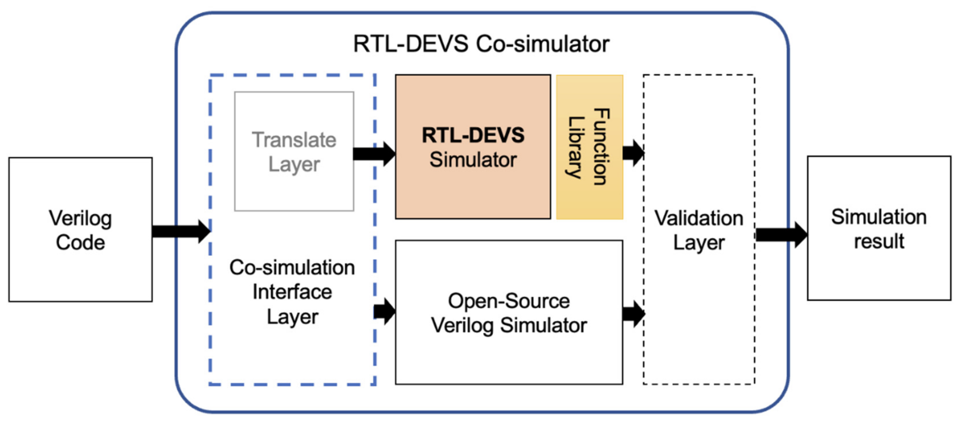
As shown in Figure 2, when we receive the Verilog description as input data, we simultaneously assign it to a DEVS format-based simulator and an open-source simulator. The final goal is to develop the RTL-DEVS co-simulator, which simulates high-cost functions that require additional development instead of using commercial RTL design tools and simulates other functions using an open-source RTL tool. Verilog descriptions have already been confirmed to be transferable to other tools via XML several times, and SCXML (State Chart XML) and DEVS2VHDL can be converted from DEVS to HDL code [7].
In this paper, we describe a methodology for designing hardware and performing gate-level synthesis and simulation in a development environment based on the DEVS format. The DEVS formalism, which includes computation and time, enables efficient and optimized design processes. By simplifying abstract hardware specifications, the DEVS simulator validates them and when the desired results are obtained, a system architect can proceed with the design process using the HDL tool. Section 2 describes the prerequisites for performing RTL simulations based on DEVS formalism. Section 3 deals with environmental modeling for RTL-DEVS simulations, and Section 4 deals with simulation results for basic component verification.
2. Hardware Representation Requirements
A common approach to hardware design is to use HDL, which is like Verilog. The hardware-level design consists of logic and register specifications for performing the behavior of each module in a complex circuit diagram, and is represented by a finite state machine. A DEVS model with an iterative cycle repeats the process of outputting events every second and transitions back to the corresponding state. HDL models are also a set having the same behavior, but they have clock cycles and timer interfaces representing more complex specifications. Therefore, simulations of HDL models in the DEVS simulator must meet requirements similar to the RTL representation level. Verilog HDL is based on principles similar commonly used programming languages and should be capable of multiple layers of design representation. It can also be used for a variety of purposes at various stages of the design process, and at the top level, it should be possible to validate system functionality through behavioral-level modeling.
2.1. HDL Requirement
To perform HDL simulation on a DEVS-based simulator, the following requirements must be satisfied. To simulate a combination and sequential circuit in a digital system, (1) the output to the input must be representable, and (2) the transport delay of the circuit is required to express and simulate of the combination circuit. (3) For the representation and simulation of sequential circuits, it should be possible to express the state representation, state transition, output transition, and timing properties for state transition. Table 1 shows the requirements of HDL simulation to be guaranteed by RTL-DEVS.
HDL-based design begins by specifying the interface port of the module. The operation of the module is then determined by calculations based on input signals and internal variables, and the output is allocated from calculated or stored values. The hierarchical model framework and interface underlying DEVS formalism are compatible with hardware technical languages such as Verilog HDL. For HDL simulations, abstraction levels must be able to guarantee representations of concurrency and state transitions, and hierarchical and modular methodologies are required to invoke pre-designed modules [8].
Our research aims to support front-end-level System IC design between specifications and HDL simulation during HDL Design. The RTL-DEVS simulation component is divided into two components: testbench design for RTL Design and verification and synthetic RTL modeling.
2.2. DEVS Formalism for Verilog Semantics
The DEVS (Discrete Event System Specification) formalism introduced by Zeigler is a set-theoretic formalism which provides a means of modeling a discrete event system in a hierarchical, modular way. With DEVS formalism, we can perform system modeling more easily by breaking down huge hierarchical systems into small component model units that are interconnected and interactive. There are two types of models in DEVS formalism.
The atomic model is the most basic model that can no longer be decomposed in DEVS-based design specifications. The atomic model describes the change in the behavior and state of a component over time. Formally, an atomic model M is specified by a septuple as follows:
M = <X, S, Y, δ int, δ ext, λ, ta>
where X is the set of input values.
S is a set of states.
Y is the set of output values.
δ int: S → S is the internal transition function.
δ ext: Q × Xb → S is the external transition function,
where Q ∈ {(s,e) | s ∈ S, 0 ≤ e ≤ ta(s)} is the total state set,
e is the time elapsed since last transition,
Xb denotes the collection of bags over X.
λ: S → Yb is the output function.
ta: S → R + 0, is the time advance function
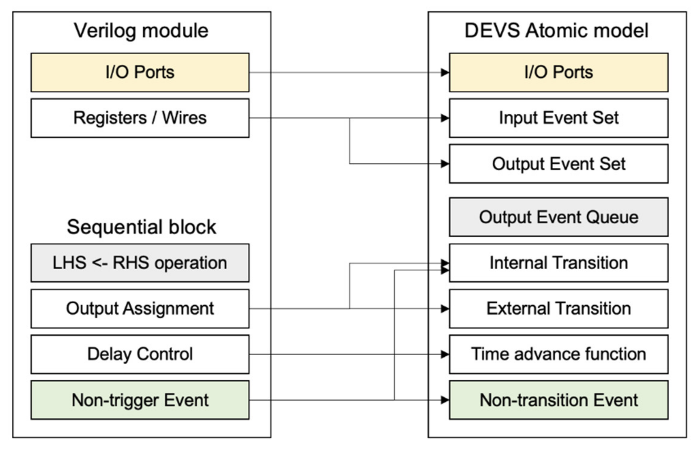
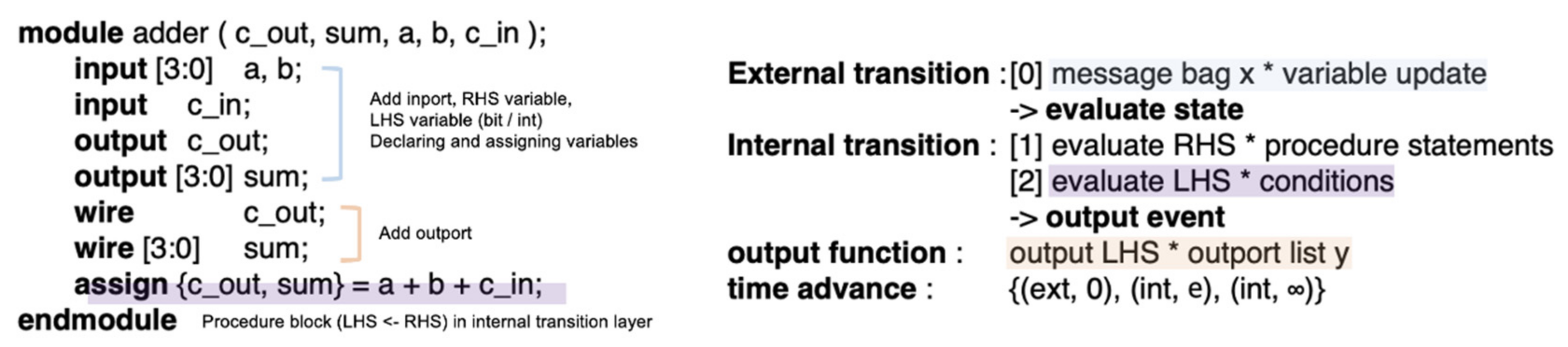
The septuple DEVS model is the most commonly used form. When matched with the Verilog module, X matches the input wire/register list and trigger that activates the always statement. S is common to all atomic models clk/wire input → (S2, δint(0)) 0-time internal transition followed by logical operations and event queues, output wire update → (S3, δext(t)) wire (Y) output. Then, time advance by timescale → (S1, δint(infinity)) has an input wait. The components of the atomic model corresponding to the Verilog module with one procedure module are shown in Figure 3.
DEVS formalism uses a coupled model to represent the entire system hierarchically. This model can construct a complex model by combining multiple atomic models into one to create a new model. The definition of the coupling model DN is as follows:
DN = < X, Y, D, EIC, EOC, IC, SELECT >
where
X: input events set
Y: output events set
D: set of all component models in DEVS
EIC ⊆ X × ∪iXi: external input coupling relation
EOC ⊆ ∪iYi × Y: external output coupling relation
IC ⊆ ∪iXi ×∪iYi: internal coupling relation
SELECT: 2M - φ -> D is a function which chooses one model when more than two models are scheduled simultaneously.
The coupled model is required when multiple atomic model groups, i.e., multiple modules, are used in a single simulation. The output signal from one module is transmitted to the appropriate DN model with reference to D, and to the atomic model inside the coupled model with reference to IC. Each model has both EIC and EOC that manage internal input/output. Such a coupled model can be basically used to simulate multiple modules within one testbench, but it is also necessary to ensure an installation that mixes submodules within the modules.
Additionally, expressing and performing an HDL simulation with DEVS formalism must be accompanied by a confluent transition function on what state and how to respond when internal transition occurs and race conditions occur due to message input from the outside. In previous studies, the concept of Delta-time advance, as with HDL simulators, has been introduced to generate minute time advancements that are expressed on the simulator but not shown in the actual simulation results. In RTL-DEVS, the concept of Delta-time was not applied because the entire atomic model was controlled according to the clk frequency of the testbench, and all atomic models performed the same transition/output procedure in time. However, DEVS formalism guarantees a fairly high degree of freedom for the expansion of specifications, so it can be expanded as necessary.
2.3. RTL-DEVS Atomic Model
2.3.1. Model I/O Control and Transitions
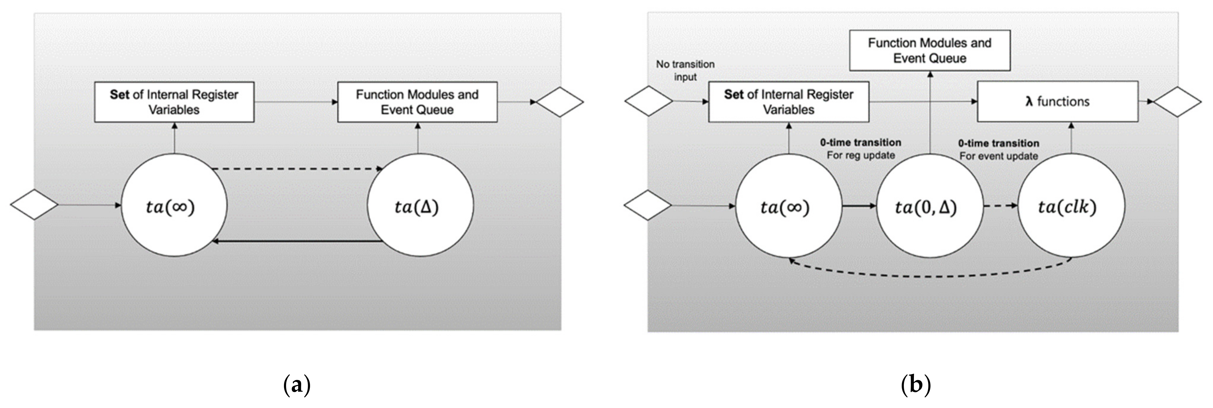
Figure 4a shows the transition process of the atomic model that was previously used to define HDEVS. Figure 4b shows the atomic model of RTL-DEVS with a total of three states as an extension of HDEVS. The RTL-DEVS model can apply almost all functions of the Verilog module described above. The input ports of the model define the events that the atomic model will respond to, and the output ports define the events that can be raised by the model. The internal transition process defines how the state of the model will change according to internal and external events. External transition means that the state is changed by an external input. At this time, the input signal ((posedge, negedege, always) clk, rst), etc. belonging to the transition condition of the atomic model operates the internal procedure block of the module, and a 0-time transition occurs. On the other hand, inputs that do not belong to the transition conditions, such as internal register values (in_0, in_1, reg1[0:3]..), are ignored until the next scheduled output event.
2.3.2. Positive and Negative Edge Trigger
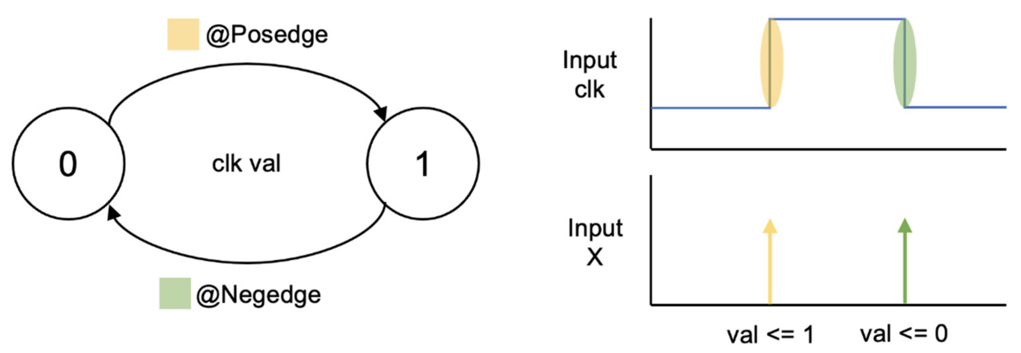
Each atomic model has function modules, which means the model’s behavior, and can generate a register update and wire output for input every simulation time. At the same time, another atomic model ported to the aforementioned atomic model receives a wire output as an input, updates the register, and generates a wire output. The atomic model updates register information corresponding to the input port to true for 0-time via external transitions for signals entered at the same time. And through the internal transition for 0-time, the function result for each register is outputted from the output port as an output wire.When configuring a combined model by connecting multiple atomic models, careful arrangement is required to prevent race conditions. A 0-time transition and a timeout internal transition are used to distinguish between posedge and negedge. When a simulation in units of 1ns is performed, the external transition of the atomic model updates the register value corresponding to the signal bag entered in the input port. If reg = 0 is updated to reg = 1, posedge occurs, and if reg = 1 is updated to reg = 0, negedge occurs. Figure 5 describes a process in which the value of the internal variable clk is changed when message X is inputted to the input port of the atomic model due to the application of clk to the testbench.
2.3.3. Procedure Block Processing between External/Internal Transition
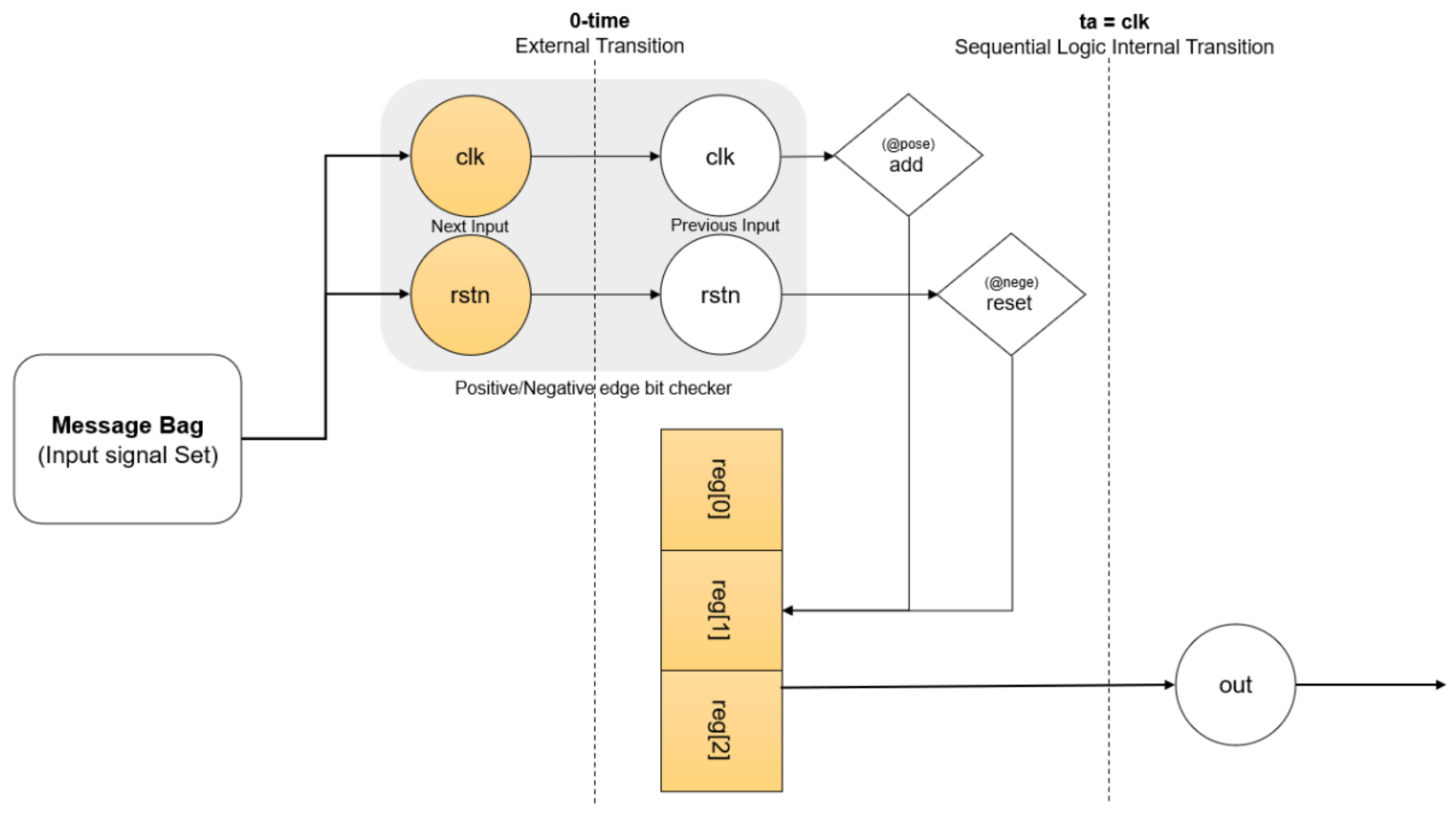
Figure 6 describes the situation in which the signal of the out wire is updated by executing the procedure block during the internal/external transition and transition process of the atomic model given the input signal set. The moment the 0-time transition occurs, the atomic model can distinguish the previous state (current value) and the future state (new value). Internal variables in RTL-DEVS are part of the state of the atomic model expressed as integer values in the current implementation, and are updated before the actual time advance occurs. The 0-time internal transition between 0-time external transition and clk time transition is the part that monitors the occurrence of a transition or output event and can mimic the behavior of the procedure block using conditional statements. For output events after clk time transition, all LHS (left hand side) and RHS (right hand side) operations are performed through conditional statements before the output event occurs, and the LHS results are exported through the outport wire for the finally determined variable.
Figure 7 shows the variable assignment of a single atomic model and the behavioral structure of atomic model functions {external transition, internal transition, output function, time advance} in the DEVS-based simulation environment.
2.3.4. Delay Control
Basically, the delay time in Verilog is divided into two models: transport delay and inertial delay. Inertial delay has been proposed to model gates or circuits that do not transfer short pulses from input to output. If the gate has a delay time of t, the pulse signal with a width shorter than t is ignored. The transport delay is intended to model the delay time that occurs in the wiring due to various physical factors. In other words, when an input change occurs, the input change is received, but the actual output is scheduled after a defined time. This delay time is processed based on the event queue, RHS, and LHS values that the Verilog simulator has internally. The active event queue performs logical operations on events that the Verilog module must process at the current time and output the result to the outport.
In DEVS formalism, the state transition of the model can be performed by processing the event of the active state based on each state and time advance. The non-blocking event queue exists to assign the RHS value calculated from the active event queue to the non-blocking assignment. Similarly, since the signal delivered to the input port in the RTL-DEVS model maintains the previous RHS value, it is possible to flexibly respond to non-blocking and blocking. The postponed queue stores the event occurrence time for the corresponding delay when there is a scheduled delay output.
Figure 8 shows how the delay time model works in the RTL-DEVS model for a typical time slot in a Verilog simulation. Inertial delay is the default delay of Verilog HDL, and if the width of the change in the input signal is less than the specified delay value, the change in the input signal does not affect the output. In order to apply the inertial delay to the RTL-DEVS model, a transition occurs due to an external transition event, and when a logic operation occurs, it is necessary to evaluate the RHS value and compare it with the value to be assigned to the LHS. After performing RHS evaluation in the current time slot, the process of comparing whether it matches with the RHS value in the postponed queue is performed. If the RHS value is different from the value scheduled to be assigned to the postponed queue, the scheduled assignment event is canceled. If the new RHS value is the same as the current value of the LHS, a separate event does not occur and is added to the postponed queue to reserve the next time slot. Conversely, if the new RHS value is different from the current LHS value, the event is generated after the delay time of the event queue. In the case of transport delay, it will not immediately export the LHS value from the active event queue/non-blocking queue to the output port, and it will receive the LHS from the postponed queue and pass it to the output port.
In RTL-DEVS, all I/O signals can receive the LHS value of the previous module as an input message at the beginning and end of each time slot, or they can send out the value assigned to the LHS variable in the atomic model. All exchanges are made using message entities compatible across all modules.
3. Testbench Modeling for RTL-DEVS Model Simulation
In tests using Verilog and HDL languages, a testbench that can deliver signals for clk, rst, enable, etc. is used instead of the main function. Unlike Verilog modules that describe the behavior of actual modules, testbench places each module at the top level for hardware simulation and secures the connectivity between each module. After that, the waveform of the signal should be grasped during the simulation time to determine whether the correct value has been obtained. The minimum simulation time (time scale) is limited to 1ns due to performance issues.
3.1. Sequential Logic Simulation Testbench
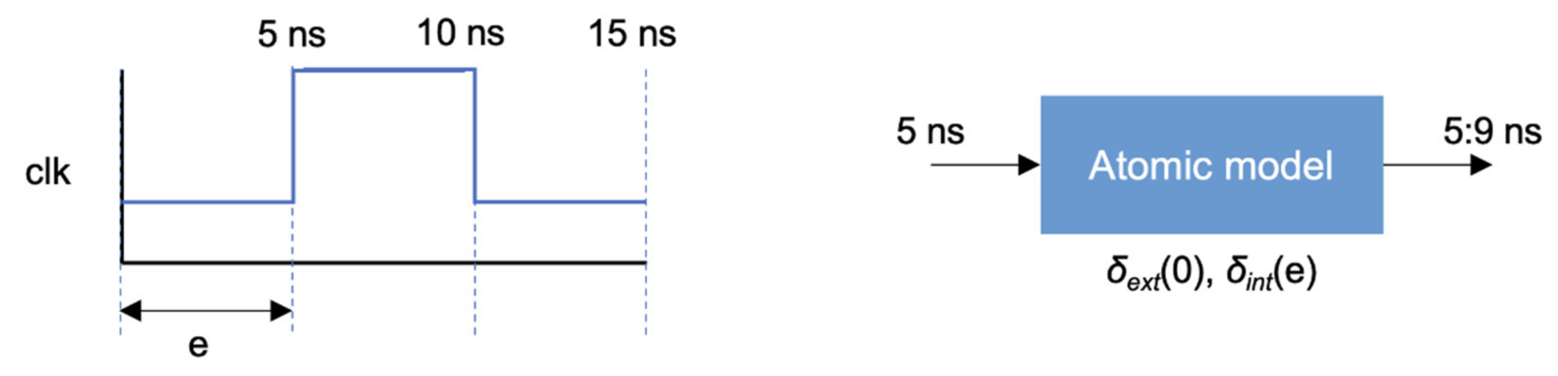
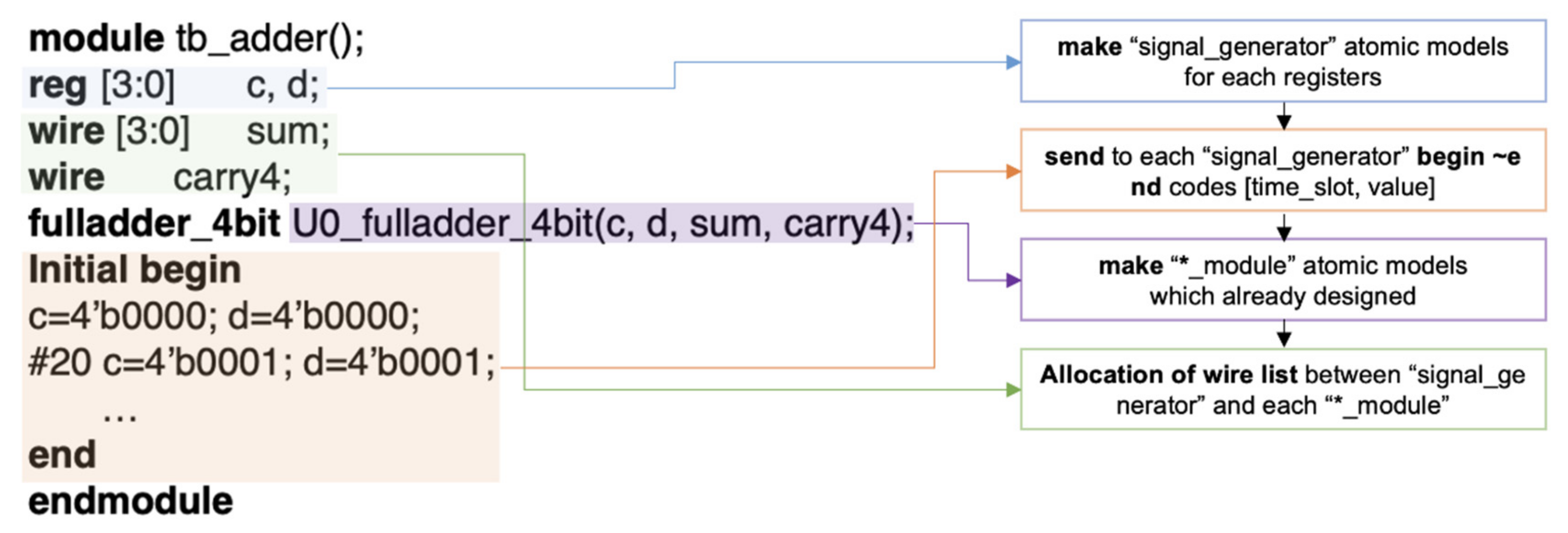
Figure 9 shows the process in which the 10ns clk output of the testbench and the half-cycle of the signal are delivered to the atomic model in the form of (e) in a sequential logic simulation where a time-based simulation is performed. If the upper edge signal is inputted at 5ns, the atomic model reserves the signal output between 5ns and 9ns through the internal transition process and waits for the next input signal. The process in which the testbench transmits the signal including clk to the module set <M> on the testbench through wire or net is by the signal generator between the begin ~ end statements assigned by the testbench. The signal generator determines the initial state during the initial process and transmits a wire value to each atomic model. Furthermore, the corresponding state changes according to the conditional statement written in testbench and the progress of time, so that the behavior of the atomic model changes. Figure 10 below briefly describes the relationship between the testbench and RTL-DEVS atomic model in the entire simulation model and the arrangement of signal generators.
3.2. Cominational Logic Simulation Testbench
The time-based concept does not apply to the design of a combination logic circuit, so the output appears only through a combination of current inputs. Therefore, the designer can operate the assigned statement of the designed module by allocating the input wire value of the connected module within the begin ~ end of the testbench model after placing the predefined module. In combinational logic, delay control in sequential logic and time/threshold-based time advance by an always statement are not required, so all transitions are performed in 0-time. When the user applies combinational logic and sequential logic at the same time, it does not generate warnings or errors, so the appropriate throw handling is required when applying the RTL-DEVS model to each DEVS-based environment.
3.3. Testbench Digraph Model Representation
Figure 11 shows the process of placing each detailed element of Verilog code in the testbench model. In DEVS formalism, the testbench is expressed as a digraph model for simulation, which plays the same role as the main() function area in programming. The testbench model requires the arrangement of the pre-designed RTL-DEVS atomic model, the arrangement of the signal generator model to deliver events to each atomic model at a specified time, and the connection of the wire list.
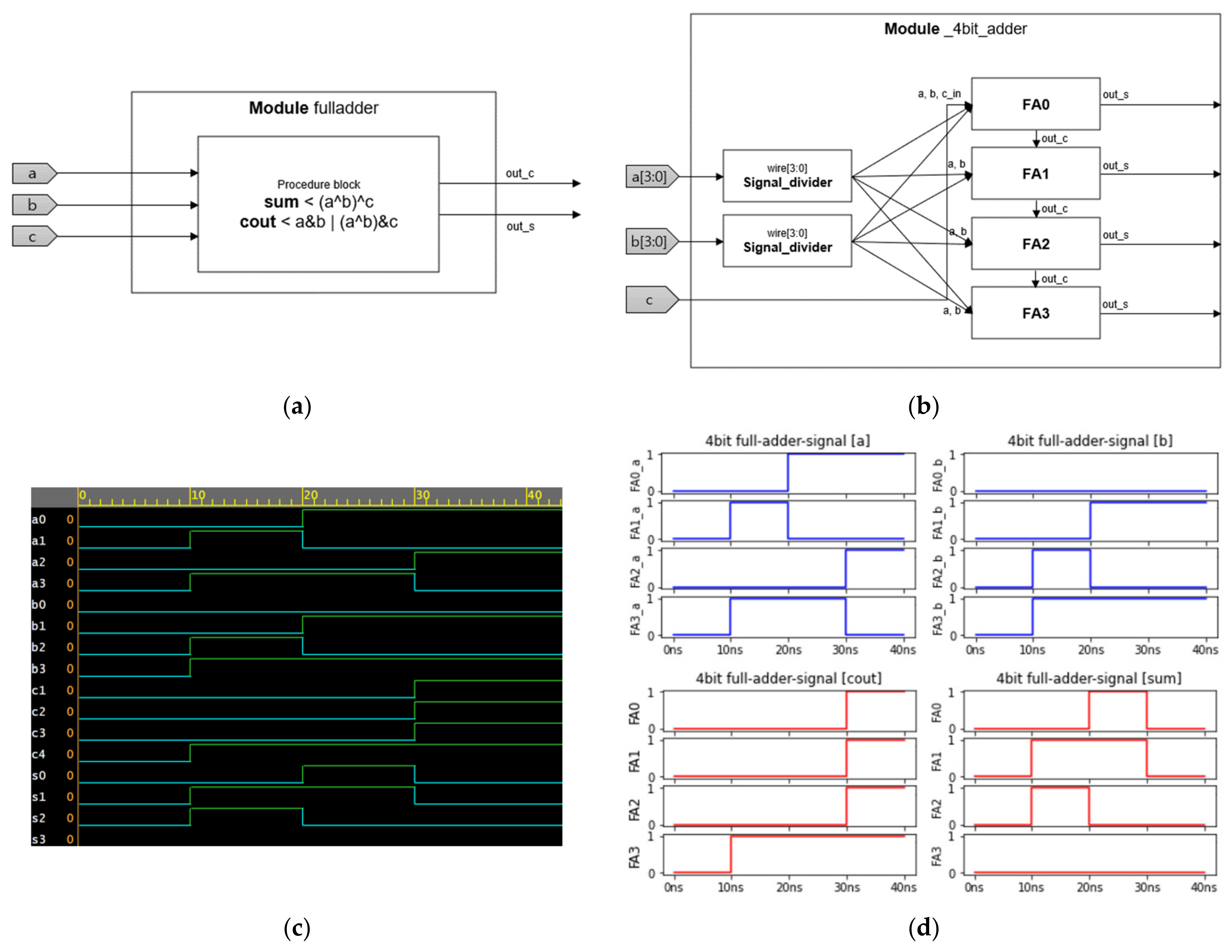
Figure 12 shows the testbench model of a 4bit-full-adder with four submodules as an example. Two signal generators {c, d} send a message out at the timing assigned by the testbench. Module U0 processes the message received through the input port or transmits it to submodule {U0:U3}. Each submodule processes the message received through the input port {a, b, c} internally and sends it to the output port {carry, sum} at the next simulation time.
4. Experimental Results of RTL-DEVS Abstract Simulation
This section deals with the results of verification that Verilog simulation requirements are met based on the extended RTL-DEVS model in the DEVS model. The validation consisted of four elements: logic gate-level simulations are not commonly used in Verilog design and simulation, but if the logic gate level can be handled, the combination logic is also scalable. Combination logic is not a time-based simulation and can be simulated with discrete events. If time slots and active event queues are properly implemented in the model, sequential logic can be simulated in the form of a mixture of discrete events + discrete times. The model was designed and simulated in a DEVSJAVA environment.
4.1. Logic-Gate Level Simulation Result
In logic gate simulation in Figure 13, the most basic module half adder is implemented and simulated. At first, we must design the gate-primitive atomic models XOR and AND shown in Figure 13a. In gate primitive models, it just receives input signals and returns an rhs operation result immediately. As shown in Figure 13b, when a model receives a message bag x, check input lists and assign signal values to RHS variables. After assigning RHS, external transition occurred, and there was a transition to an “operation” state. In the operation state, the LHS operation and internal transition is executed. In the last “output” state, a wire output is executed and then returns to the initial “wait” state. This state means that the module is paused indefinitely until the next signal received. For simulating this model, two signal generator atomic models were used. Figure 13c,d shows that the half adder coupled model works as designed.
4.2. Combinational Logic Simulation Result
Figure 14 shows the model digraph and simulation results of the combinational logic simulation model full-adder and 4-bit-adder. In Figure 14a, module FA (full-adder) was specified first, and a 4-bit adder was specified based on the specified full adder. In the Verilog HDL, variables with multiple wires are expressed in vector [0:n] form. Although it is possible to deliver a vector-type signal directly to submodules, a signal divider model that divides a vector signal into 1-bit format is placed at the input port of the module for more appropriate internal processing. In the case of combinatorial logic, such as gate level logic, the register does not remember past inputs and executes logic operations only with current input signals. Due to such characteristics, when multiple submodules are used, multiple input signal updates occurred in the current time slot. For example, in the 30ns simulation time in Figure 14d, FA2 has sum as an output when it first receives the input signal set (a:1, b:0, c:0), but FA1 has c_out as a result of logic operation, and the c:1 signal update occurs by FA1 output. As a result, the sum at 30 ns of FA2 becomes 0, and c_out becomes 1. Therefore, it seems necessary to have a signal determinant with a delta-time latency in a model design if the module has multiple submodules and it outputs logic operation signals immediately to other modules. Figure 14c,d show that the Verilog simulation results and the RTL-DEVS simulation can output equivalent results. However, unlike sequential logic, models that are not specified in detail have the potential to malfunction in that multiple input signal updates occur in the same time slot. After that point, the waveforms were equal.
4.3. Sequential Logic Simulation Result
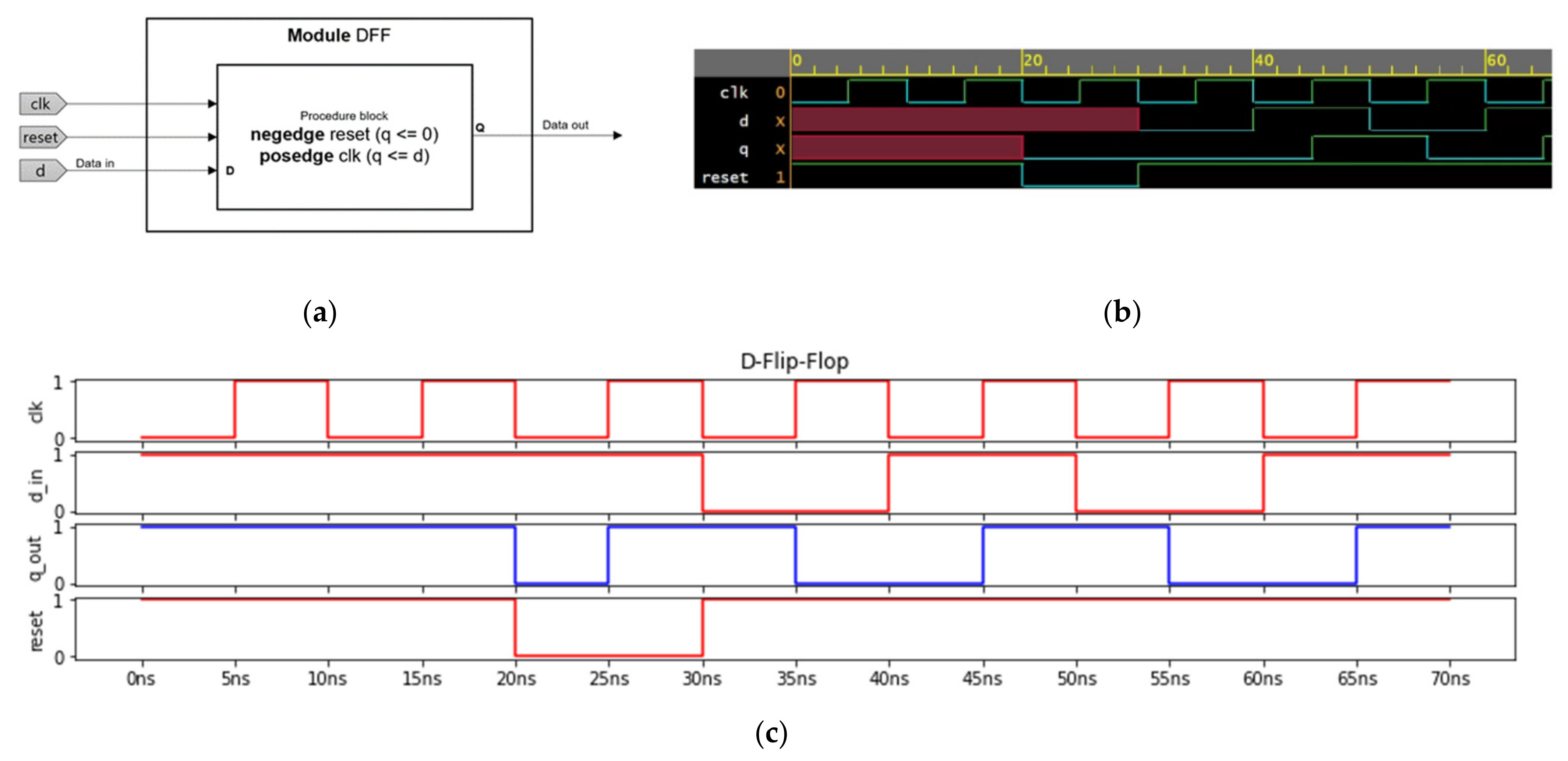
DEVS formalism which is based on discrete events and time advance best matches design and simulates a sequential logic circuit. In Figure 15, (a) shows the operation specification of the module for DFF (D-flip-flop), one of the most famous sequential circuits, and the design of the testbench. The biggest characteristic when specifying the operation of this module in the atomic model is that the state transition for signal output occurs only when the posedge clk or negedge reset condition of the always statement is satisfied. For other signal inputs, the RHS value changes, but the LHS value does not change immediately because no external transition occurred. The output q of DFF has the characteristic of reflecting the value of input d to output q when posedge clk occurs. In Figure 15c, the 25ns simulation time point shows a difference in q value compared to Figure 15b. Because d contains x value when the d value is assigned to q due to posedge trigger, q also has unknown x until the next posedge trigger work.
4.4. Time Delay Simulation Result
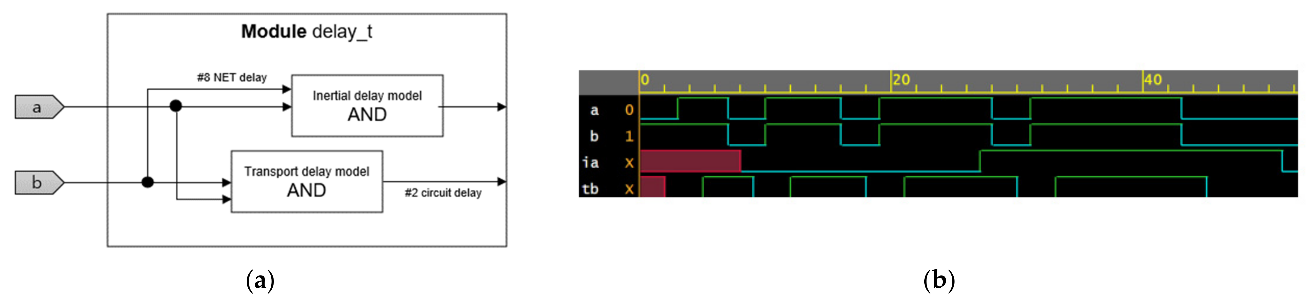
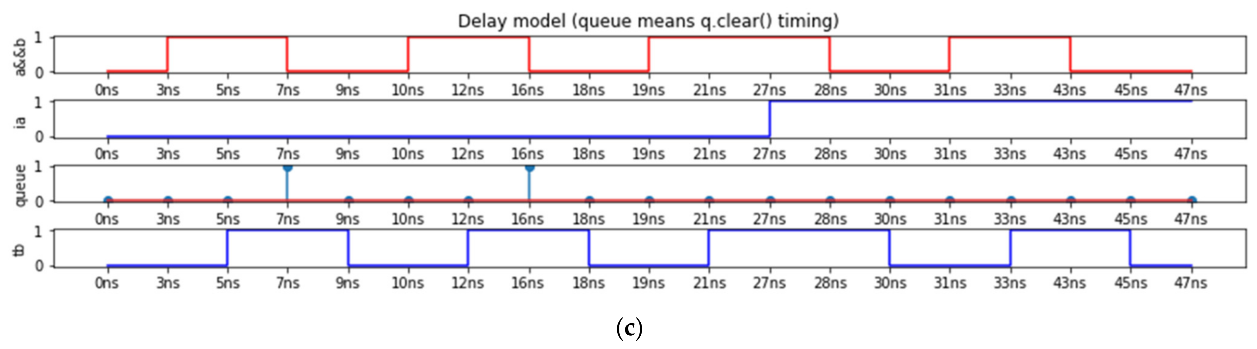
In a simulation with delay time in Figure 16, unlike other models, the entire system is observed with a time step of 1 ns. Each model has a “sigma” that can know its current time slot as a key variable. When RHS evaluation is completed and 1 is assigned to LHS by a conditional statement, delay time is added to the sigma and put into the queue. The clear difference between inertial delay and transport delay is that the inertial delay queue is emptied if the enqueue does not occur continuously as long as delay time, whereas the transport delay event is unconditionally assigned to output LHS after delay time. In Figure 16b,c, tb with a 2ns transport delay outputs a&b high after 2ns. And the ia with 8ns initial delay remains low until it reaches 27ns. The delay time model designed using RTL-DEVS seems to work well at first glance, but unlike the other models, it has a problem with losing consistency in that it requires time slot-based simulations in steps of 1ns.
In conclusion, attempts to apply RTL simulation to DEVS formalism are sufficiently capable of design and simulation at the abstract level in the form of RTL-DEVS, except the signal noise problem at the combinational logic level and the 1ns stepping time slot of the time delay model. When comparing waveform and step graphs, equivalence was confirmed for almost all points.
However, in this study, there is a limitation in comparing equality using only elementary logic blocks. The coupled model expressed as RTL-DEVS solves the control of timing and logic through a method of temporarily allocating the RHS and LHS variables of each atomic model, but in the case of complex circuits, the coupled model contains many other coupled models, so probability of defects is high due to timing control. It is necessary to additionally consider that output messages can be delivered simultaneously. In Pifer’s study [7], this problem could be solved by using the handshaker atomic model, which temporarily stores signal messages on the input wire of each module and informs the coordinator of the simulation engine that a signal has been received.
5. Conclusions and Future Works
In this work, we implemented RTL-DEVS by leveraging the functionality of DEVS formalism-based modeling for hardware design. Through the designed RTL-DEVS model and simulation testbench, Verilog’s timing control, netlist presentation, and abstract level simulation test were performed, and the simulation model could be expanded through the implementation of the simulation model and the waveform output of the testbench.
Hardware design using RTL-DEVS, which can be continuously extended through the advancement of model specifications, suggests that simulations using extended libraries are possible in the limited environment of Verilog. DEVS formalism-based modeling is easily adaptable and translatable to other DEVS-based simulation environments, such as via XML, so it can be applied to multiple designs. In addition, it enables simulator development and plug-and-play model exchange through the addition of various languages, scalable classes, and test benches.
As the complexity and size of modern developed SOCs (System on Chips) increases, verification becomes more important than design. Verification technologies are also evolving, and high scalability or automated methodologies such as UVM (Universal Verification Methodology) are becoming more important points for semiconductor chip development. Combining high-level language tools leveraging expertise in sequential programming for the validation of designed modules provides a design experience using an easily scalable and reusable DEVS format for the specification of hardware behavior and enables the use of sequential languages such as C for operations.
The design and specification of the model based on DEVS formalism shows that it can be used as a simulation tool when it goes through the elaboration process. but for exhaustive simulations such as sequential equivalence checking, it faces the daunting task that commercial-level simulators must analyze in detail the functions supported by the commercial-level simulator and express them in DEVS formalism.
Future research directions are to improve the RTL-DEVS model so that more expressions are possible, and to enable equivalence verification through the grafting of the Verilog to DEVS formalism tool under development.
Author Contributions
Conceptualization, Y.-S.H.; methodology, B.-S.K.; software, B.-S.K.; validation, B.-S.K.; formal analysis, B.-S.K.; investigation, Y.-D.N.; writing original draft preparation, Y.-D.N.; writing, S.-W.J.; review and editing, S.-W.J.; supervision, J.-S.L.; project administration, J.-S.L.; funding acquisition, Y.-S.H. All authors have read and agreed to the published version of the manuscript.
Funding
This research was supported by the National Research Foundation of Korea (NRF) grant funded by the Korea government funded by the Ministry of Science, ICT and Future Planning (NRF-2021R1A2C1003122).
Data Availability Statement
Not applicable.
Conflicts of Interest
The authors declare that they have no conflicts of interest.
References
- Tallaksen, E. UVVM—The Fastest Growing FPGA Verification Methodology Worldwide! In Proceedings of the 2019 Workshop on Open Source Design Automation (OSDA), 2019 Design, Automation and Test in Europe Conference (DATE), Florence, Italy, 29 March 2019; Available online: https://osda.gitlab.io/19/tallaksen.pdf (accessed on 25 November 2020).
- Muñoz-Quijada, M.; Sanz, L.; Guzman-Miranda, H. SW-VHDL Co-Verification Environment Using Open Source Tools. Electronics 2020, 9, 2104. [Google Scholar] [CrossRef]
- Molter, H.G.; Seffrin, A.; Huss, S.A. DEVS2VHDL: Automatic Transformation of XML specified DEVS Model of Computation into Synthesizable VHDL Code. In Proceedings of the 12th Forum on Specification and Design Languages (FDL 2009), Sophia Antipolis, France, 22–24 September 2009. [Google Scholar]
- Kwon, S.J.; Sung, C.; Song, H.S.; Kim, T.G. Integrated Hybrid Modeling Methodology and Simulation Engine Design Based on HDEVS Formalism. J. Korea Soc. Simul. 2013, 22, 21–30. [Google Scholar] [CrossRef] [Green Version]
- Kim, T.G.; Kim, J.K.; Kim, Y.G. DHMIF: DEVS-based hardware model interchange format. In Proceedings of the European Simulation Symposium, Marseille, France, 18–20 October 2001. [Google Scholar]
- Jiang, S.; Pan, P.; Ou, Y.; Batten, C. PyMTL3: A Python Framework for Open-Source Hardware Modeling, Generation, Simulation, and Verification. IEEE Micro 2020, 40, 58–66. [Google Scholar] [CrossRef]
- Pifer, T.J. DEVS-Based Hardware Design, Synthesis, and Power Optimization Using Explicit Time Specifications and Deterministic Path-Based Latency. Master’s Thesis, University of Arizona, Tucson, AZ, USA, 2012. [Google Scholar]
- Seo, C.; Zeigler, B.P.; Coop, R.; Kim, D. DEVS modeling and simulation methodology with MS4 Me software tool. In Proceedings of the Symposium on Theory of Modeling & Simulation—DEVS Integrative M&S Symposium (DEVS 13), Society for Computer Simulation International, San Diego, CA, USA, 7–10 April 2013; pp. 1–8. [Google Scholar]
Figure 1.
High scalability of DEVS-based specifications.

Figure 2.
Abstract specification of RTL-DEVS co-simulator.

Figure 3.
Hardware model to atomic DEVS model mapping-based behavioral module.

Figure 4.
(a) Overview of atomic model specification; (b) Model specification for RTL-DEVS.

Figure 5.
Edge trigger processing in inner variable of atomic model.

Figure 6.
Internal state transition representation. It shows 0-time transition for RHS operation.

Figure 7.
Converting and defining the Verilog module to the RTL-DEVS atomic model.

Figure 8.
Formal Verilog simulator time slot procedure and RTL-DEVS delay model time slot.

Figure 9.
e is elapsed time of DEVS time advance. It works on end of atomic model’s state cycle.

Figure 10.
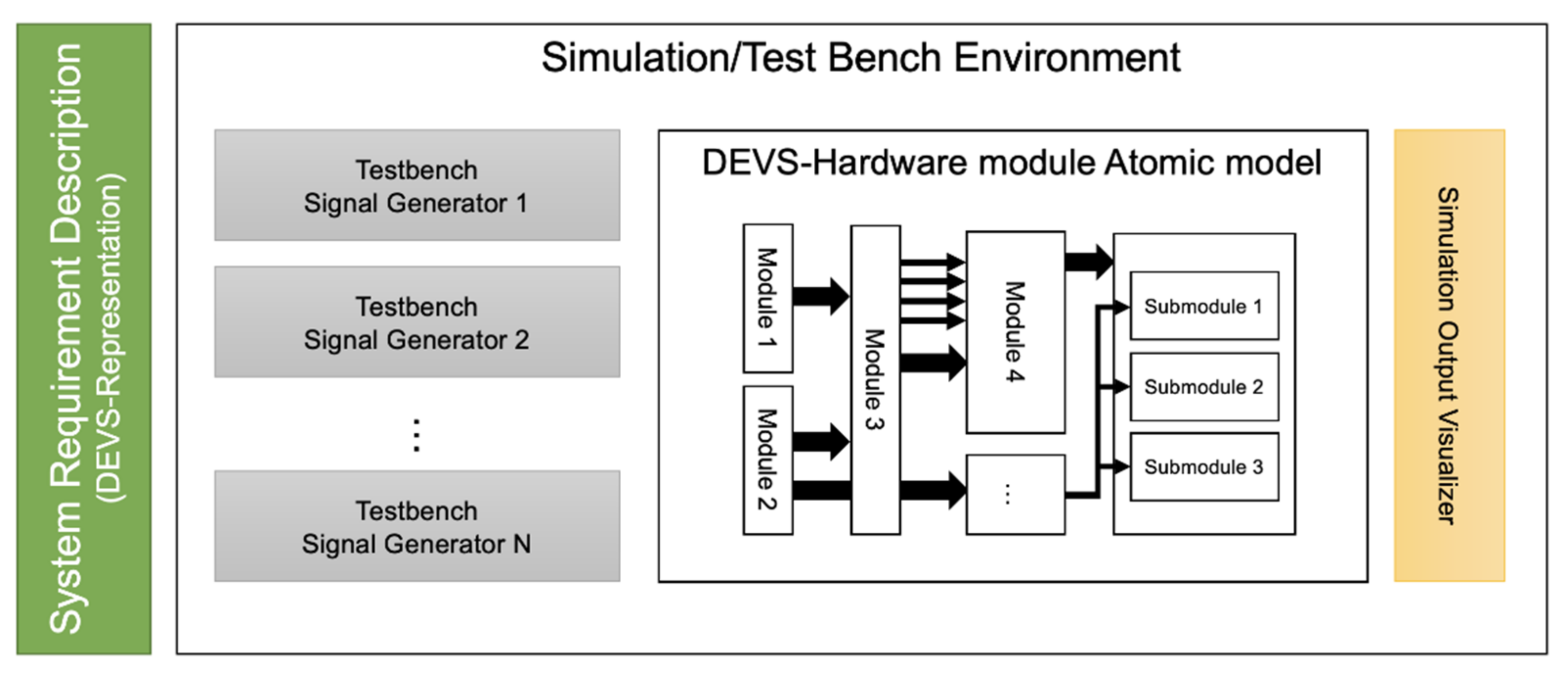
Overview of DEVS-based modeling and simulation methodology.

Figure 11.
Testbench DEVS-diagraph model representation.

Figure 12.
Visualized overview of RTL-DEVS testbench module and atomic modules.

Figure 13.
Logic gate model simulation components, which should be listed as: (a) description of half adder module; (b) gate primitive model states and transition; (c) EPWave transform of original Verilog half adder module; and (d) RTL-DEVS simulation result step graph.
Figure 13.
Logic gate model simulation components, which should be listed as: (a) description of half adder module; (b) gate primitive model states and transition; (c) EPWave transform of original Verilog half adder module; and (d) RTL-DEVS simulation result step graph.

Figure 14.
Combinational logic model simulation components, which should be listed as: (a) Description of full adder submodule; (b) Description of 4bit full adder module; (c) EPWave transform of original Verilog 4bit full adder module; and (d) RTL-DEVS simulation result step graph.
Figure 14.
Combinational logic model simulation components, which should be listed as: (a) Description of full adder submodule; (b) Description of 4bit full adder module; (c) EPWave transform of original Verilog 4bit full adder module; and (d) RTL-DEVS simulation result step graph.

Figure 15.
Sequential logic model simulation components, which should be listed as: (a) Description of D-Flip-Flop module; (b) EPWave transform of original Verilog DFF module; (c) RTL-DEVS simulation result step graph.
Figure 15.
Sequential logic model simulation components, which should be listed as: (a) Description of D-Flip-Flop module; (b) EPWave transform of original Verilog DFF module; (c) RTL-DEVS simulation result step graph.

Figure 16.
Delay time based model simulation components, they should be listed as: (a) Description of delay test module; (b) EPWave transform of original Verilog delay_t module (c) RTL-DEVS simulation result step graph.
Figure 16.
Delay time based model simulation components, they should be listed as: (a) Description of delay test module; (b) EPWave transform of original Verilog delay_t module (c) RTL-DEVS simulation result step graph.


Table 1.
Requirements for Representing Hardware Models.
| Aspect | Requirements | |
|---|---|---|
| Sequential/ Combinational | Combinational | Output evaluation for the input with delay (feedback free, no state) |
| Sequential | State representation, state transition, timing for state transition | |
| Synthesis | RTL description | State representation, state transition with timing property |
| Gate-level description | Gate behavior with propagation delay, network of gates | |
| Level of Abstraction | Behavioral | Concurrency, state transition |
| Structural | Modular/hierarchical modeling | |
| Others | Formal verification, Separation of interface and behavior | |
Disclaimer/Publisher’s Note: The statements, opinions and data contained in all publications are solely those of the individual author(s) and contributor(s) and not of MDPI and/or the editor(s). MDPI and/or the editor(s) disclaim responsibility for any injury to people or property resulting from any ideas, methods, instructions or products referred to in the content. |
© 2022 by the authors. Licensee MDPI, Basel, Switzerland. This article is an open access article distributed under the terms and conditions of the Creative Commons Attribution (CC BY) license (https://creativecommons.org/licenses/by/4.0/).
Share and Cite
MDPI and ACS Style
Kwon, B.-S.; Jung, S.-W.; Noh, Y.-D.; Lee, J.-S.; Han, Y.-S. RTL-DEVS: HDL Design and Simulation Methodology for DEVS Formalism-Based Simulation Tool. Telecom 2023, 4, 15-30. https://doi.org/10.3390/telecom4010002
AMA Style
Kwon B-S, Jung S-W, Noh Y-D, Lee J-S, Han Y-S. RTL-DEVS: HDL Design and Simulation Methodology for DEVS Formalism-Based Simulation Tool. Telecom. 2023; 4(1):15-30. https://doi.org/10.3390/telecom4010002
Chicago/Turabian StyleKwon, Bo-Seung, Sang-Won Jung, Young-Dan Noh, Jong-Sik Lee, and Young-Shin Han. 2023. "RTL-DEVS: HDL Design and Simulation Methodology for DEVS Formalism-Based Simulation Tool" Telecom 4, no. 1: 15-30. https://doi.org/10.3390/telecom4010002